EP3788677B1 - Diélectrique à faible coût pour une transmission électrique et antenne utilisant ce dernier - Google Patents
Diélectrique à faible coût pour une transmission électrique et antenne utilisant ce dernier Download PDFInfo
- Publication number
- EP3788677B1 EP3788677B1 EP18917499.8A EP18917499A EP3788677B1 EP 3788677 B1 EP3788677 B1 EP 3788677B1 EP 18917499 A EP18917499 A EP 18917499A EP 3788677 B1 EP3788677 B1 EP 3788677B1
- Authority
- EP
- European Patent Office
- Prior art keywords
- plate
- dielectric
- dielectric constant
- antenna
- layer
- Prior art date
- Legal status (The legal status is an assumption and is not a legal conclusion. Google has not performed a legal analysis and makes no representation as to the accuracy of the status listed.)
- Active
Links
Images


Classifications
-
- H—ELECTRICITY
- H01—ELECTRIC ELEMENTS
- H01Q—ANTENNAS, i.e. RADIO AERIALS
- H01Q3/00—Arrangements for changing or varying the orientation or the shape of the directional pattern of the waves radiated from an antenna or antenna system
- H01Q3/26—Arrangements for changing or varying the orientation or the shape of the directional pattern of the waves radiated from an antenna or antenna system varying the relative phase or relative amplitude of energisation between two or more active radiating elements; varying the distribution of energy across a radiating aperture
- H01Q3/30—Arrangements for changing or varying the orientation or the shape of the directional pattern of the waves radiated from an antenna or antenna system varying the relative phase or relative amplitude of energisation between two or more active radiating elements; varying the distribution of energy across a radiating aperture varying the relative phase between the radiating elements of an array
- H01Q3/34—Arrangements for changing or varying the orientation or the shape of the directional pattern of the waves radiated from an antenna or antenna system varying the relative phase or relative amplitude of energisation between two or more active radiating elements; varying the distribution of energy across a radiating aperture varying the relative phase between the radiating elements of an array by electrical means
- H01Q3/36—Arrangements for changing or varying the orientation or the shape of the directional pattern of the waves radiated from an antenna or antenna system varying the relative phase or relative amplitude of energisation between two or more active radiating elements; varying the distribution of energy across a radiating aperture varying the relative phase between the radiating elements of an array by electrical means with variable phase-shifters
-
- H—ELECTRICITY
- H01—ELECTRIC ELEMENTS
- H01P—WAVEGUIDES; RESONATORS, LINES, OR OTHER DEVICES OF THE WAVEGUIDE TYPE
- H01P1/00—Auxiliary devices
- H01P1/18—Phase-shifters
- H01P1/184—Strip line phase-shifters
-
- H—ELECTRICITY
- H01—ELECTRIC ELEMENTS
- H01Q—ANTENNAS, i.e. RADIO AERIALS
- H01Q1/00—Details of, or arrangements associated with, antennas
- H01Q1/36—Structural form of radiating elements, e.g. cone, spiral, umbrella; Particular materials used therewith
- H01Q1/38—Structural form of radiating elements, e.g. cone, spiral, umbrella; Particular materials used therewith formed by a conductive layer on an insulating support
-
- H—ELECTRICITY
- H01—ELECTRIC ELEMENTS
- H01Q—ANTENNAS, i.e. RADIO AERIALS
- H01Q3/00—Arrangements for changing or varying the orientation or the shape of the directional pattern of the waves radiated from an antenna or antenna system
- H01Q3/44—Arrangements for changing or varying the orientation or the shape of the directional pattern of the waves radiated from an antenna or antenna system varying the electric or magnetic characteristics of reflecting, refracting, or diffracting devices associated with the radiating element
-
- H—ELECTRICITY
- H01—ELECTRIC ELEMENTS
- H01Q—ANTENNAS, i.e. RADIO AERIALS
- H01Q9/00—Electrically-short antennas having dimensions not more than twice the operating wavelength and consisting of conductive active radiating elements
- H01Q9/04—Resonant antennas
- H01Q9/0407—Substantially flat resonant element parallel to ground plane, e.g. patch antenna
- H01Q9/0442—Substantially flat resonant element parallel to ground plane, e.g. patch antenna with particular tuning means
-
- H—ELECTRICITY
- H01—ELECTRIC ELEMENTS
- H01Q—ANTENNAS, i.e. RADIO AERIALS
- H01Q9/00—Electrically-short antennas having dimensions not more than twice the operating wavelength and consisting of conductive active radiating elements
- H01Q9/04—Resonant antennas
- H01Q9/0407—Substantially flat resonant element parallel to ground plane, e.g. patch antenna
- H01Q9/045—Substantially flat resonant element parallel to ground plane, e.g. patch antenna with particular feeding means
-
- H—ELECTRICITY
- H05—ELECTRIC TECHNIQUES NOT OTHERWISE PROVIDED FOR
- H05K—PRINTED CIRCUITS; CASINGS OR CONSTRUCTIONAL DETAILS OF ELECTRIC APPARATUS; MANUFACTURE OF ASSEMBLAGES OF ELECTRICAL COMPONENTS
- H05K1/00—Printed circuits
- H05K1/02—Details
- H05K1/03—Use of materials for the substrate
- H05K1/0313—Organic insulating material
- H05K1/0353—Organic insulating material consisting of two or more materials, e.g. two or more polymers, polymer + filler, + reinforcement
- H05K1/036—Multilayers with layers of different types
-
- H—ELECTRICITY
- H01—ELECTRIC ELEMENTS
- H01Q—ANTENNAS, i.e. RADIO AERIALS
- H01Q21/00—Antenna arrays or systems
- H01Q21/06—Arrays of individually energised antenna units similarly polarised and spaced apart
- H01Q21/061—Two dimensional planar arrays
- H01Q21/065—Patch antenna array
-
- H—ELECTRICITY
- H05—ELECTRIC TECHNIQUES NOT OTHERWISE PROVIDED FOR
- H05K—PRINTED CIRCUITS; CASINGS OR CONSTRUCTIONAL DETAILS OF ELECTRIC APPARATUS; MANUFACTURE OF ASSEMBLAGES OF ELECTRICAL COMPONENTS
- H05K1/00—Printed circuits
- H05K1/02—Details
- H05K1/0213—Electrical arrangements not otherwise provided for
- H05K1/0237—High frequency adaptations
Definitions
- circuit board with microstrip printed technology Common methods of conducting electromagnetic energy between locations are to use a circuit board with microstrip printed technology or using a metallic wave-guide.
- the advantage of a circuit board over a waveguide is that it can be produced in higher volumes and is flat.
- the disadvantage is the loss which is proportional to the distance the high frequency electronic signal travels.
- the advantage of a metallic wave-guide is that it operates with lower losses, but the disadvantage is that it is neither as thin as a circuit board nor as cost effective.
- circuit board substrates are designed to have low propagation losses.
- the typical low loss substrate is a mixture of Teflon and glass.
- these Circuit Boards are more expensive because of the process of pressing the Teflon and glass flat, which requires tremendous pressure.
- Teflon ® Polytetrafluoroethylene
- Teflon A further disadvantage of Teflon is its high cost. In many modem applications the entire transmission circuitry needs to be of very low cost, which makes Teflon prohibitive.
- Variable DC potential is applied across the VDC plate to control the effective dielectric constant at various locations of the VDC plate.
- RF signal is coupled between a feed patch and a delay line, and the delay line couples the RF signal to the radiating patch.
- the radiating patch, VDC plate, delay line, and feed patch are each provided at a different layer of the antenna, so as to decouple the RF and DC signal paths.
- a controller executes a software program to thereby control the variable DC potential applied across the VDC plate, thereby controlling the operational characteristics of the antenna.
- US 2010/060535 A1 relates to a microstrip patch antenna for mobile satellite communications comprising a first electrically conducting ground plane having at least one opening, at least one patch radiating element, at least one first dielectric layer, disposed between the first electrically conducting ground plane and the patch radiating element and more particularly between the at least one opening and the patch radiating element, at least one feed line for providing signal energy in a contactless manner to or from the patch radiating element through the opening and a second dielectric layer disposed between the feed line and the first electrically conducting ground plane wherein the antenna further comprises a second ground plane and a third dielectric layer disposed between the second ground plane and the feed line.
- an antenna as defined in claim 1 is provided.
- the antenna may further comprise conductive electrodes abutting the VDC layer.
- At least one of: the insulating spacer, the dielectric plate, and the bottom insulating plate, may comprise a foam plate sandwiched between two glass plates or a foam plate sandwiched between two PET plates.
- the antenna may further comprise at least one conductive via connecting each one of the delay lines to a corresponding radiating patch.
- the ground plane can comprise at least one window, each aligned below a corresponding one of the radiating patches.
- a radiating device comprising: a dielectric plate; a conductive ground plane formed on bottom surface of the dielectric plate; and a radiating element formed on top surface of the dielectric plate; wherein the dielectric plate comprises a plate of glass and a plate of foam.
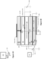
- variable dielectric constant (VDC) plate 440 having variable dielectric constant material 444. While any manner for constructing the VDC plate 440 may be suitable for use with the embodiments of the antenna, as a shorthand in the specific embodiments the VDC plate 440 is shown consisting of upper binder 442, (e.g., glass, PET, etc.) variable dielectric constant material 444 (e.g., twisted nematic liquid crystal layer), and bottom binder 446. In other embodiments one or both of the binder layers 442 and 444 may be omitted. Alternatively, adhesive such as epoxy or glass beads may be used instead of the binder layers 442 and/or 444.
- binder 442 e.g., glass, PET, etc.
- variable dielectric constant material 444 e.g., twisted nematic liquid crystal layer
- bottom binder 446 e.g., twisted nematic liquid crystal layer
- adhesive such as epoxy or glass beads may be used instead of the binder layers 442 and/or 444.
- the VDC plate 440 also includes an alignment layer that may be deposited and/or glued onto the bottom of the upper binder 442.
- the alignment layer may be a thin layer of material, such as polyimide-based PVA, that is being rubbed or cured with UV radiation in order to align the molecules of the LC at the edges of confining substrates.
- the effective dielectric constant of VDC plate 440 can be controlled by applying DC potential across the VDC plate 440.
- electrodes are formed and are connected to controllable voltage potential.
- controllable voltage potential There are various arrangements to form the electrodes, and several examples will be shown in the disclosed embodiments.
- electrode 447 is shown connected to variable voltage potential 441, while electrode 443 is connected to ground.
- electrode 443 may also be connected to a variable potential 439.
- variable potential 441 and/or variable potential 439 by changing the output voltage of variable potential 441 and/or variable potential 439, one can change the dielectric constant of the VDC material in the vicinity of the electrodes 443 and 447, and thereby change the RF signal traveling over delay line 415.
- Changing the output voltage of variable potential 441 and/or variable potential 439 can be done using a controller, Ctl, running software that causes the controller to output the appropriate control signal to set the appropriate output voltage of variable potential 441 and/or variable potential 439.
- a conventional controller can be used to provide the control and common signals to control the characteristics of the antenna.
- the antenna's performance and characteristics can be controlled using software - hence software controlled antenna.
- the embodiments disclosed herein can be used for radiating elements, such as antennas and antenna arrays.
- electronic devices or components can also be provided, which have variable electrical characteristics or operation based on potential applied to a variable-dielectric constant sector associated with the device and incorporate the low-cost dielectric sandwich.
- the electronic devices or component may include bends, power splitters, filters, ports, phase shifters, frequency shifters, attenuators, couplers, capacitors, inductors, diplexers, hybrids of beam forming networks, and may also include radiating elements in addition to the electronic devices.
- several devices can be formed on the same dielectric sandwich, just like was done in the prior art using Rogers ® or PCP.
- Element 527 is the variable dielectric constant material, that receive potential from power supplier V.
- the conductive line 520 is formed on top of a dielectric plate 550, that may be made according to any of the embodiments disclosed herein. For example, it may be made of a sandwich of glass plate and foam plate.
Landscapes
- Engineering & Computer Science (AREA)
- Microelectronics & Electronic Packaging (AREA)
- Waveguide Aerials (AREA)
- Details Of Aerials (AREA)
- Waveguides (AREA)
- Variable-Direction Aerials And Aerial Arrays (AREA)
Claims (10)
- Antenne, comprenant :une plaque diélectrique (400) ;au moins une plaque rayonnante (410) disposée par-dessus la plaque diélectrique (400) ;au moins une ligne à retard (415) disposée sous la plaque diélectrique (400) ;dans laquelle la plaque diélectrique (400) comprend au moins une première couche à constante diélectrique élevée (402) ayant une constante diélectrique de 3,8 à 4,4 et une première plaque de mousse (404) contiguës l'une à l'autre,une couche à constante diélectrique variable (444) disposée sous la ligne à retard (415) ;un plan de masse (455) disposé sous la couche à constante diélectrique variable (444) ;une plaque isolante inférieure (450) disposée sous le plan de masse (455) ; et,une ligne d'alimentation (460) disposée sous la plaque isolante inférieure (450) ;dans laquelle la plaque isolante inférieure (450) comprend une deuxième plaque de mousse (454) prise en sandwich entre deux plaques de verre (452 ; 456) ou une deuxième plaque de mousse (454) prise en sandwich entre deux plaques de poly(téréphtalate d'éthylène) (452 ; 456).
- Antenne selon la revendication 1, dans laquelle l'au moins une première couche à constante diélectrique élevée (402) est formée de verre.
- Antenne selon la revendication 1, dans laquelle l'au moins une première couche à constante diélectrique élevée (402) est formée de poly(téréphtalate d'éthylène).
- Antenne selon la revendication 1, dans laquelle la première plaque de mousse (404) est formée pour avoir une constante diélectrique de 1,0 à 1,1.
- Antenne selon la revendication 1, dans laquelle la plaque diélectrique (400) comprend une couche supérieure de poly(téréphtalate d'éthylène) et une couche inférieure de poly(téréphtalate d'éthylène), dans laquelle la première plaque de mousse (404) est prise en sandwich entre la couche supérieure de poly(téréphtalate d'éthylène) et la couche inférieure de poly(téréphtalate d'éthylène).
- Antenne selon la revendication 1, dans laquelle la couche à constante diélectrique variable (440) comprend un matériau à constante diélectrique variable (444) et au moins un liant supérieur (442) et un liant inférieur (446).
- Antenne selon la revendication 6, dans laquelle l'un ou les deux du liant supérieur (442) et du liant inférieur (446) comprend ou comprennent au moins une seconde couche à constante diélectrique élevée (449) ayant une constante diélectrique de 3,8 à 4,4 et une troisième plaque de mousse (448).
- Antenne selon la revendication 1, comprenant en outre des électrodes conductrices (443) en butée avec le matériau à constante diélectrique variable (444).
- Antenne selon la revendication 1, comprenant en outre au moins un via conducteur (425) connectant chacune des lignes à retard (415) à une plaque rayonnante (410) correspondante.
- Antenne selon la revendication 1, dans laquelle le plan de masse (455) comprend au moins une fenêtre (453), chaque fenêtre étant alignée sous une plaque correspondante des plaques rayonnantes (410).
Applications Claiming Priority (1)
| Application Number | Priority Date | Filing Date | Title |
|---|---|---|---|
| PCT/US2018/030529 WO2019212542A1 (fr) | 2018-05-01 | 2018-05-01 | Diélectrique à faible coût pour une transmission électrique et antenne utilisant ce dernier |
Publications (3)
| Publication Number | Publication Date |
|---|---|
| EP3788677A1 EP3788677A1 (fr) | 2021-03-10 |
| EP3788677A4 EP3788677A4 (fr) | 2021-12-15 |
| EP3788677B1 true EP3788677B1 (fr) | 2024-07-10 |
Family
ID=68387022
Family Applications (1)
| Application Number | Title | Priority Date | Filing Date |
|---|---|---|---|
| EP18917499.8A Active EP3788677B1 (fr) | 2018-05-01 | 2018-05-01 | Diélectrique à faible coût pour une transmission électrique et antenne utilisant ce dernier |
Country Status (6)
| Country | Link |
|---|---|
| EP (1) | EP3788677B1 (fr) |
| JP (1) | JP2021530881A (fr) |
| KR (1) | KR102623151B1 (fr) |
| CN (1) | CN112204817B (fr) |
| CA (1) | CA3101948A1 (fr) |
| WO (1) | WO2019212542A1 (fr) |
Family Cites Families (13)
| Publication number | Priority date | Publication date | Assignee | Title |
|---|---|---|---|---|
| US4783666A (en) * | 1987-05-21 | 1988-11-08 | General Electric Company | Protective shield for an antenna array |
| JPH06140822A (ja) * | 1991-07-04 | 1994-05-20 | Panatsuku Kogyo Kk | 平面型アンテナ |
| DE19615497A1 (de) * | 1996-03-16 | 1997-09-18 | Pates Tech Patentverwertung | Planarer Strahler |
| US6903541B2 (en) * | 2001-05-25 | 2005-06-07 | Tyco Electronics Corporation | Film-based microwave and millimeter-wave circuits and sensors |
| US8368596B2 (en) * | 2004-09-24 | 2013-02-05 | Viasat, Inc. | Planar antenna for mobile satellite applications |
| JP2008515253A (ja) * | 2004-09-24 | 2008-05-08 | ジャスト・サール | モバイル衛星応用対象のためのプレーナ・アンテナ |
| CN101479887A (zh) * | 2006-05-24 | 2009-07-08 | 韦夫班德尔公司 | 集成波导管天线和阵列 |
| US8743006B2 (en) * | 2007-10-31 | 2014-06-03 | Nitta Corporation | Wireless communication-improving sheet member, wireless IC tag, antenna, and wireless communication system using the same |
| US20110163921A1 (en) * | 2010-01-06 | 2011-07-07 | Psion Teklogix Inc. | Uhf rfid internal antenna for handheld terminals |
| EP2768072A1 (fr) * | 2013-02-15 | 2014-08-20 | Technische Universität Darmstadt | Déphaseur |
| US9273989B2 (en) | 2014-03-28 | 2016-03-01 | Honeywell International Inc. | Foam filled dielectric rod antenna |
| US10686257B2 (en) * | 2016-09-01 | 2020-06-16 | Wafer Llc | Method of manufacturing software controlled antenna |
| US10326205B2 (en) * | 2016-09-01 | 2019-06-18 | Wafer Llc | Multi-layered software defined antenna and method of manufacture |
-
2018
- 2018-05-01 CA CA3101948A patent/CA3101948A1/fr active Pending
- 2018-05-01 KR KR1020207031962A patent/KR102623151B1/ko active Active
- 2018-05-01 WO PCT/US2018/030529 patent/WO2019212542A1/fr not_active Ceased
- 2018-05-01 CN CN201880092910.3A patent/CN112204817B/zh active Active
- 2018-05-01 EP EP18917499.8A patent/EP3788677B1/fr active Active
- 2018-05-01 JP JP2020560996A patent/JP2021530881A/ja active Pending
Also Published As
| Publication number | Publication date |
|---|---|
| EP3788677A4 (fr) | 2021-12-15 |
| EP3788677A1 (fr) | 2021-03-10 |
| KR20210062593A (ko) | 2021-05-31 |
| JP2021530881A (ja) | 2021-11-11 |
| CN112204817A (zh) | 2021-01-08 |
| KR102623151B1 (ko) | 2024-01-09 |
| CA3101948A1 (fr) | 2019-11-07 |
| CN112204817B (zh) | 2025-04-11 |
| WO2019212542A1 (fr) | 2019-11-07 |
Similar Documents
| Publication | Publication Date | Title |
|---|---|---|
| US10511096B2 (en) | Low cost dielectric for electrical transmission and antenna using same | |
| EP3507858B1 (fr) | Antenne multicouches définie par logiciel | |
| EP3704760B1 (fr) | Modulateur de phase à cristaux liquides multicouches | |
| JP7424977B2 (ja) | 液晶移相器およびその操作方法、液晶アンテナ、通信機器 | |
| EP4016733B1 (fr) | Structure d'alimentation, dispositif de radiofréquence à micro-ondes et antenne | |
| EP3745527B1 (fr) | Déphaseur à cristaux liquides, antenne à cristaux liquides, et procédé de fabrication de déphaseur à cristaux liquides | |
| CN110574236A (zh) | 一种液晶可重构多波束相控阵列 | |
| US20230163481A1 (en) | Liquid crystal antena and fabrication thereof | |
| US20180159239A1 (en) | Low loss electrical transmission mechanism and antenna using same | |
| JP2019530387A (ja) | ビーム・ステアリング・アンテナのための液晶調整可能メタサーフェス | |
| CN112448106A (zh) | 馈电结构、微波射频器件及天线 | |
| CN110235301B (zh) | 基于液晶的高频装置和高频开关 | |
| EP3788677B1 (fr) | Diélectrique à faible coût pour une transmission électrique et antenne utilisant ce dernier | |
| CN116565486A (zh) | 移相器、移相器阵列、天线及电子设备 | |
| CN117134119A (zh) | 天线、电子设备及天线的制备方法 | |
| TWI680876B (zh) | 用於電傳輸的低成本介電質及使用該介電質的天線 |
Legal Events
| Date | Code | Title | Description |
|---|---|---|---|
| STAA | Information on the status of an ep patent application or granted ep patent |
Free format text: STATUS: THE INTERNATIONAL PUBLICATION HAS BEEN MADE |
|
| PUAI | Public reference made under article 153(3) epc to a published international application that has entered the european phase |
Free format text: ORIGINAL CODE: 0009012 |
|
| STAA | Information on the status of an ep patent application or granted ep patent |
Free format text: STATUS: REQUEST FOR EXAMINATION WAS MADE |
|
| 17P | Request for examination filed |
Effective date: 20201201 |
|
| AK | Designated contracting states |
Kind code of ref document: A1 Designated state(s): AL AT BE BG CH CY CZ DE DK EE ES FI FR GB GR HR HU IE IS IT LI LT LU LV MC MK MT NL NO PL PT RO RS SE SI SK SM TR |
|
| AX | Request for extension of the european patent |
Extension state: BA ME |
|
| DAV | Request for validation of the european patent (deleted) | ||
| DAX | Request for extension of the european patent (deleted) | ||
| REG | Reference to a national code |
Ref country code: DE Ref legal event code: R079 Free format text: PREVIOUS MAIN CLASS: H01Q0021060000 Ipc: H01Q0003360000 Ref country code: DE Ref legal event code: R079 Ref document number: 602018071725 Country of ref document: DE Free format text: PREVIOUS MAIN CLASS: H01Q0021060000 Ipc: H01Q0003360000 |
|
| A4 | Supplementary search report drawn up and despatched |
Effective date: 20211115 |
|
| RIC1 | Information provided on ipc code assigned before grant |
Ipc: H05K 1/02 20060101ALN20211109BHEP Ipc: H01Q 21/06 20060101ALN20211109BHEP Ipc: H05K 1/03 20060101ALI20211109BHEP Ipc: H01P 1/18 20060101ALI20211109BHEP Ipc: H01Q 1/38 20060101ALI20211109BHEP Ipc: H01Q 9/04 20060101ALI20211109BHEP Ipc: H01Q 3/36 20060101AFI20211109BHEP |
|
| STAA | Information on the status of an ep patent application or granted ep patent |
Free format text: STATUS: EXAMINATION IS IN PROGRESS |
|
| 17Q | First examination report despatched |
Effective date: 20230307 |
|
| RIC1 | Information provided on ipc code assigned before grant |
Ipc: H05K 1/02 20060101ALN20231222BHEP Ipc: H01Q 21/06 20060101ALN20231222BHEP Ipc: H05K 1/03 20060101ALI20231222BHEP Ipc: H01P 1/18 20060101ALI20231222BHEP Ipc: H01Q 1/38 20060101ALI20231222BHEP Ipc: H01Q 9/04 20060101ALI20231222BHEP Ipc: H01Q 3/36 20060101AFI20231222BHEP |
|
| GRAP | Despatch of communication of intention to grant a patent |
Free format text: ORIGINAL CODE: EPIDOSNIGR1 |
|
| STAA | Information on the status of an ep patent application or granted ep patent |
Free format text: STATUS: GRANT OF PATENT IS INTENDED |
|
| RIC1 | Information provided on ipc code assigned before grant |
Ipc: H05K 1/02 20060101ALN20240108BHEP Ipc: H01Q 21/06 20060101ALN20240108BHEP Ipc: H05K 1/03 20060101ALI20240108BHEP Ipc: H01P 1/18 20060101ALI20240108BHEP Ipc: H01Q 1/38 20060101ALI20240108BHEP Ipc: H01Q 9/04 20060101ALI20240108BHEP Ipc: H01Q 3/36 20060101AFI20240108BHEP |
|
| RIC1 | Information provided on ipc code assigned before grant |
Ipc: H05K 1/02 20060101ALN20240124BHEP Ipc: H01Q 21/06 20060101ALN20240124BHEP Ipc: H05K 1/03 20060101ALI20240124BHEP Ipc: H01P 1/18 20060101ALI20240124BHEP Ipc: H01Q 1/38 20060101ALI20240124BHEP Ipc: H01Q 9/04 20060101ALI20240124BHEP Ipc: H01Q 3/36 20060101AFI20240124BHEP |
|
| INTG | Intention to grant announced |
Effective date: 20240206 |
|
| GRAS | Grant fee paid |
Free format text: ORIGINAL CODE: EPIDOSNIGR3 |
|
| GRAA | (expected) grant |
Free format text: ORIGINAL CODE: 0009210 |
|
| STAA | Information on the status of an ep patent application or granted ep patent |
Free format text: STATUS: THE PATENT HAS BEEN GRANTED |
|
| AK | Designated contracting states |
Kind code of ref document: B1 Designated state(s): AL AT BE BG CH CY CZ DE DK EE ES FI FR GB GR HR HU IE IS IT LI LT LU LV MC MK MT NL NO PL PT RO RS SE SI SK SM TR |
|
| REG | Reference to a national code |
Ref country code: CH Ref legal event code: EP |
|
| REG | Reference to a national code |
Ref country code: DE Ref legal event code: R096 Ref document number: 602018071725 Country of ref document: DE |
|
| P01 | Opt-out of the competence of the unified patent court (upc) registered |
Free format text: CASE NUMBER: APP_40816/2024 Effective date: 20240710 |
|
| REG | Reference to a national code |
Ref country code: LT Ref legal event code: MG9D |
|
| REG | Reference to a national code |
Ref country code: NL Ref legal event code: MP Effective date: 20240710 |
|
| PG25 | Lapsed in a contracting state [announced via postgrant information from national office to epo] |
Ref country code: PT Free format text: LAPSE BECAUSE OF FAILURE TO SUBMIT A TRANSLATION OF THE DESCRIPTION OR TO PAY THE FEE WITHIN THE PRESCRIBED TIME-LIMIT Effective date: 20241111 |
|
| REG | Reference to a national code |
Ref country code: AT Ref legal event code: MK05 Ref document number: 1702870 Country of ref document: AT Kind code of ref document: T Effective date: 20240710 |
|
| PG25 | Lapsed in a contracting state [announced via postgrant information from national office to epo] |
Ref country code: NL Free format text: LAPSE BECAUSE OF FAILURE TO SUBMIT A TRANSLATION OF THE DESCRIPTION OR TO PAY THE FEE WITHIN THE PRESCRIBED TIME-LIMIT Effective date: 20240710 |
|
| PG25 | Lapsed in a contracting state [announced via postgrant information from national office to epo] |
Ref country code: PT Free format text: LAPSE BECAUSE OF FAILURE TO SUBMIT A TRANSLATION OF THE DESCRIPTION OR TO PAY THE FEE WITHIN THE PRESCRIBED TIME-LIMIT Effective date: 20241111 Ref country code: NL Free format text: LAPSE BECAUSE OF FAILURE TO SUBMIT A TRANSLATION OF THE DESCRIPTION OR TO PAY THE FEE WITHIN THE PRESCRIBED TIME-LIMIT Effective date: 20240710 |
|
| PG25 | Lapsed in a contracting state [announced via postgrant information from national office to epo] |
Ref country code: NO Free format text: LAPSE BECAUSE OF FAILURE TO SUBMIT A TRANSLATION OF THE DESCRIPTION OR TO PAY THE FEE WITHIN THE PRESCRIBED TIME-LIMIT Effective date: 20241010 |
|
| PG25 | Lapsed in a contracting state [announced via postgrant information from national office to epo] |
Ref country code: GR Free format text: LAPSE BECAUSE OF FAILURE TO SUBMIT A TRANSLATION OF THE DESCRIPTION OR TO PAY THE FEE WITHIN THE PRESCRIBED TIME-LIMIT Effective date: 20241011 Ref country code: FI Free format text: LAPSE BECAUSE OF FAILURE TO SUBMIT A TRANSLATION OF THE DESCRIPTION OR TO PAY THE FEE WITHIN THE PRESCRIBED TIME-LIMIT Effective date: 20240710 Ref country code: PL Free format text: LAPSE BECAUSE OF FAILURE TO SUBMIT A TRANSLATION OF THE DESCRIPTION OR TO PAY THE FEE WITHIN THE PRESCRIBED TIME-LIMIT Effective date: 20240710 |
|
| PG25 | Lapsed in a contracting state [announced via postgrant information from national office to epo] |
Ref country code: BG Free format text: LAPSE BECAUSE OF FAILURE TO SUBMIT A TRANSLATION OF THE DESCRIPTION OR TO PAY THE FEE WITHIN THE PRESCRIBED TIME-LIMIT Effective date: 20240710 |
|
| PG25 | Lapsed in a contracting state [announced via postgrant information from national office to epo] |
Ref country code: LV Free format text: LAPSE BECAUSE OF FAILURE TO SUBMIT A TRANSLATION OF THE DESCRIPTION OR TO PAY THE FEE WITHIN THE PRESCRIBED TIME-LIMIT Effective date: 20240710 |
|
| PG25 | Lapsed in a contracting state [announced via postgrant information from national office to epo] |
Ref country code: IS Free format text: LAPSE BECAUSE OF FAILURE TO SUBMIT A TRANSLATION OF THE DESCRIPTION OR TO PAY THE FEE WITHIN THE PRESCRIBED TIME-LIMIT Effective date: 20241110 Ref country code: AT Free format text: LAPSE BECAUSE OF FAILURE TO SUBMIT A TRANSLATION OF THE DESCRIPTION OR TO PAY THE FEE WITHIN THE PRESCRIBED TIME-LIMIT Effective date: 20240710 |
|
| PG25 | Lapsed in a contracting state [announced via postgrant information from national office to epo] |
Ref country code: HR Free format text: LAPSE BECAUSE OF FAILURE TO SUBMIT A TRANSLATION OF THE DESCRIPTION OR TO PAY THE FEE WITHIN THE PRESCRIBED TIME-LIMIT Effective date: 20240710 |
|
| PG25 | Lapsed in a contracting state [announced via postgrant information from national office to epo] |
Ref country code: ES Free format text: LAPSE BECAUSE OF FAILURE TO SUBMIT A TRANSLATION OF THE DESCRIPTION OR TO PAY THE FEE WITHIN THE PRESCRIBED TIME-LIMIT Effective date: 20240710 Ref country code: RS Free format text: LAPSE BECAUSE OF FAILURE TO SUBMIT A TRANSLATION OF THE DESCRIPTION OR TO PAY THE FEE WITHIN THE PRESCRIBED TIME-LIMIT Effective date: 20241010 |
|
| PG25 | Lapsed in a contracting state [announced via postgrant information from national office to epo] |
Ref country code: RS Free format text: LAPSE BECAUSE OF FAILURE TO SUBMIT A TRANSLATION OF THE DESCRIPTION OR TO PAY THE FEE WITHIN THE PRESCRIBED TIME-LIMIT Effective date: 20241010 Ref country code: PL Free format text: LAPSE BECAUSE OF FAILURE TO SUBMIT A TRANSLATION OF THE DESCRIPTION OR TO PAY THE FEE WITHIN THE PRESCRIBED TIME-LIMIT Effective date: 20240710 Ref country code: NO Free format text: LAPSE BECAUSE OF FAILURE TO SUBMIT A TRANSLATION OF THE DESCRIPTION OR TO PAY THE FEE WITHIN THE PRESCRIBED TIME-LIMIT Effective date: 20241010 Ref country code: LV Free format text: LAPSE BECAUSE OF FAILURE TO SUBMIT A TRANSLATION OF THE DESCRIPTION OR TO PAY THE FEE WITHIN THE PRESCRIBED TIME-LIMIT Effective date: 20240710 Ref country code: IS Free format text: LAPSE BECAUSE OF FAILURE TO SUBMIT A TRANSLATION OF THE DESCRIPTION OR TO PAY THE FEE WITHIN THE PRESCRIBED TIME-LIMIT Effective date: 20241110 Ref country code: HR Free format text: LAPSE BECAUSE OF FAILURE TO SUBMIT A TRANSLATION OF THE DESCRIPTION OR TO PAY THE FEE WITHIN THE PRESCRIBED TIME-LIMIT Effective date: 20240710 Ref country code: GR Free format text: LAPSE BECAUSE OF FAILURE TO SUBMIT A TRANSLATION OF THE DESCRIPTION OR TO PAY THE FEE WITHIN THE PRESCRIBED TIME-LIMIT Effective date: 20241011 Ref country code: FI Free format text: LAPSE BECAUSE OF FAILURE TO SUBMIT A TRANSLATION OF THE DESCRIPTION OR TO PAY THE FEE WITHIN THE PRESCRIBED TIME-LIMIT Effective date: 20240710 Ref country code: ES Free format text: LAPSE BECAUSE OF FAILURE TO SUBMIT A TRANSLATION OF THE DESCRIPTION OR TO PAY THE FEE WITHIN THE PRESCRIBED TIME-LIMIT Effective date: 20240710 Ref country code: BG Free format text: LAPSE BECAUSE OF FAILURE TO SUBMIT A TRANSLATION OF THE DESCRIPTION OR TO PAY THE FEE WITHIN THE PRESCRIBED TIME-LIMIT Effective date: 20240710 Ref country code: AT Free format text: LAPSE BECAUSE OF FAILURE TO SUBMIT A TRANSLATION OF THE DESCRIPTION OR TO PAY THE FEE WITHIN THE PRESCRIBED TIME-LIMIT Effective date: 20240710 |
|
| REG | Reference to a national code |
Ref country code: DE Ref legal event code: R097 Ref document number: 602018071725 Country of ref document: DE |
|
| PG25 | Lapsed in a contracting state [announced via postgrant information from national office to epo] |
Ref country code: RO Free format text: LAPSE BECAUSE OF FAILURE TO SUBMIT A TRANSLATION OF THE DESCRIPTION OR TO PAY THE FEE WITHIN THE PRESCRIBED TIME-LIMIT Effective date: 20240710 Ref country code: DK Free format text: LAPSE BECAUSE OF FAILURE TO SUBMIT A TRANSLATION OF THE DESCRIPTION OR TO PAY THE FEE WITHIN THE PRESCRIBED TIME-LIMIT Effective date: 20240710 Ref country code: SM Free format text: LAPSE BECAUSE OF FAILURE TO SUBMIT A TRANSLATION OF THE DESCRIPTION OR TO PAY THE FEE WITHIN THE PRESCRIBED TIME-LIMIT Effective date: 20240710 |
|
| PGFP | Annual fee paid to national office [announced via postgrant information from national office to epo] |
Ref country code: IE Payment date: 20250324 Year of fee payment: 8 |
|
| PG25 | Lapsed in a contracting state [announced via postgrant information from national office to epo] |
Ref country code: EE Free format text: LAPSE BECAUSE OF FAILURE TO SUBMIT A TRANSLATION OF THE DESCRIPTION OR TO PAY THE FEE WITHIN THE PRESCRIBED TIME-LIMIT Effective date: 20240710 |
|
| PG25 | Lapsed in a contracting state [announced via postgrant information from national office to epo] |
Ref country code: CZ Free format text: LAPSE BECAUSE OF FAILURE TO SUBMIT A TRANSLATION OF THE DESCRIPTION OR TO PAY THE FEE WITHIN THE PRESCRIBED TIME-LIMIT Effective date: 20240710 |
|
| PGFP | Annual fee paid to national office [announced via postgrant information from national office to epo] |
Ref country code: FR Payment date: 20250321 Year of fee payment: 8 |
|
| PG25 | Lapsed in a contracting state [announced via postgrant information from national office to epo] |
Ref country code: IT Free format text: LAPSE BECAUSE OF FAILURE TO SUBMIT A TRANSLATION OF THE DESCRIPTION OR TO PAY THE FEE WITHIN THE PRESCRIBED TIME-LIMIT Effective date: 20240710 Ref country code: SK Free format text: LAPSE BECAUSE OF FAILURE TO SUBMIT A TRANSLATION OF THE DESCRIPTION OR TO PAY THE FEE WITHIN THE PRESCRIBED TIME-LIMIT Effective date: 20240710 |
|
| PLBE | No opposition filed within time limit |
Free format text: ORIGINAL CODE: 0009261 |
|
| STAA | Information on the status of an ep patent application or granted ep patent |
Free format text: STATUS: NO OPPOSITION FILED WITHIN TIME LIMIT |
|
| 26N | No opposition filed |
Effective date: 20250411 |
|
| PGFP | Annual fee paid to national office [announced via postgrant information from national office to epo] |
Ref country code: DE Payment date: 20250319 Year of fee payment: 8 |
|
| PG25 | Lapsed in a contracting state [announced via postgrant information from national office to epo] |
Ref country code: SE Free format text: LAPSE BECAUSE OF FAILURE TO SUBMIT A TRANSLATION OF THE DESCRIPTION OR TO PAY THE FEE WITHIN THE PRESCRIBED TIME-LIMIT Effective date: 20240710 |
|
| REG | Reference to a national code |
Ref country code: CH Ref legal event code: H13 Free format text: ST27 STATUS EVENT CODE: U-0-0-H10-H13 (AS PROVIDED BY THE NATIONAL OFFICE) Effective date: 20251223 |
|
| PG25 | Lapsed in a contracting state [announced via postgrant information from national office to epo] |
Ref country code: LU Free format text: LAPSE BECAUSE OF NON-PAYMENT OF DUE FEES Effective date: 20250501 |
|
| PG25 | Lapsed in a contracting state [announced via postgrant information from national office to epo] |
Ref country code: CH Free format text: LAPSE BECAUSE OF NON-PAYMENT OF DUE FEES Effective date: 20250531 |
|
| REG | Reference to a national code |
Ref country code: BE Ref legal event code: MM Effective date: 20250531 |
|
| PG25 | Lapsed in a contracting state [announced via postgrant information from national office to epo] |
Ref country code: MC Free format text: LAPSE BECAUSE OF FAILURE TO SUBMIT A TRANSLATION OF THE DESCRIPTION OR TO PAY THE FEE WITHIN THE PRESCRIBED TIME-LIMIT Effective date: 20240710 |
|
| PGFP | Annual fee paid to national office [announced via postgrant information from national office to epo] |
Ref country code: GB Payment date: 20260325 Year of fee payment: 9 |
|
| PG25 | Lapsed in a contracting state [announced via postgrant information from national office to epo] |
Ref country code: BE Free format text: LAPSE BECAUSE OF NON-PAYMENT OF DUE FEES Effective date: 20250531 |