EP3789793B1 - Optischer näherungssensor und entsprechendes betriebsverfahren - Google Patents
Optischer näherungssensor und entsprechendes betriebsverfahren Download PDFInfo
- Publication number
- EP3789793B1 EP3789793B1 EP20192064.2A EP20192064A EP3789793B1 EP 3789793 B1 EP3789793 B1 EP 3789793B1 EP 20192064 A EP20192064 A EP 20192064A EP 3789793 B1 EP3789793 B1 EP 3789793B1
- Authority
- EP
- European Patent Office
- Prior art keywords
- solid
- electric converter
- state photo
- signal
- proximity sensor
- Prior art date
- Legal status (The legal status is an assumption and is not a legal conclusion. Google has not performed a legal analysis and makes no representation as to the accuracy of the status listed.)
- Active
Links
Images


Classifications
-
- G—PHYSICS
- G01—MEASURING; TESTING
- G01S—RADIO DIRECTION-FINDING; RADIO NAVIGATION; DETERMINING DISTANCE OR VELOCITY BY USE OF RADIO WAVES; LOCATING OR PRESENCE-DETECTING BY USE OF THE REFLECTION OR RERADIATION OF RADIO WAVES; ANALOGOUS ARRANGEMENTS USING OTHER WAVES
- G01S17/00—Systems using the reflection or reradiation of electromagnetic waves other than radio waves, e.g. lidar systems
- G01S17/02—Systems using the reflection of electromagnetic waves other than radio waves
- G01S17/06—Systems determining position data of a target
- G01S17/08—Systems determining position data of a target for measuring distance only
- G01S17/32—Systems determining position data of a target for measuring distance only using transmission of continuous waves, whether amplitude-, frequency-, or phase-modulated, or unmodulated
- G01S17/36—Systems determining position data of a target for measuring distance only using transmission of continuous waves, whether amplitude-, frequency-, or phase-modulated, or unmodulated with phase comparison between the received signal and the contemporaneously transmitted signal
-
- G—PHYSICS
- G01—MEASURING; TESTING
- G01S—RADIO DIRECTION-FINDING; RADIO NAVIGATION; DETERMINING DISTANCE OR VELOCITY BY USE OF RADIO WAVES; LOCATING OR PRESENCE-DETECTING BY USE OF THE REFLECTION OR RERADIATION OF RADIO WAVES; ANALOGOUS ARRANGEMENTS USING OTHER WAVES
- G01S17/00—Systems using the reflection or reradiation of electromagnetic waves other than radio waves, e.g. lidar systems
- G01S17/02—Systems using the reflection of electromagnetic waves other than radio waves
- G01S17/06—Systems determining position data of a target
- G01S17/08—Systems determining position data of a target for measuring distance only
- G01S17/10—Systems determining position data of a target for measuring distance only using transmission of interrupted, pulse-modulated waves
-
- G—PHYSICS
- G01—MEASURING; TESTING
- G01J—MEASUREMENT OF INTENSITY, VELOCITY, SPECTRAL CONTENT, POLARISATION, PHASE OR PULSE CHARACTERISTICS OF INFRARED, VISIBLE OR ULTRAVIOLET LIGHT; COLORIMETRY; RADIATION PYROMETRY
- G01J1/00—Photometry, e.g. photographic exposure meter
- G01J1/42—Photometry, e.g. photographic exposure meter using electric radiation detectors
- G01J1/4204—Photometry, e.g. photographic exposure meter using electric radiation detectors with determination of ambient light
-
- G—PHYSICS
- G01—MEASURING; TESTING
- G01S—RADIO DIRECTION-FINDING; RADIO NAVIGATION; DETERMINING DISTANCE OR VELOCITY BY USE OF RADIO WAVES; LOCATING OR PRESENCE-DETECTING BY USE OF THE REFLECTION OR RERADIATION OF RADIO WAVES; ANALOGOUS ARRANGEMENTS USING OTHER WAVES
- G01S7/00—Details of systems according to groups G01S13/00, G01S15/00, G01S17/00
- G01S7/48—Details of systems according to groups G01S13/00, G01S15/00, G01S17/00 of systems according to group G01S17/00
- G01S7/481—Constructional features, e.g. arrangements of optical elements
- G01S7/4814—Constructional features, e.g. arrangements of optical elements of transmitters alone
- G01S7/4815—Constructional features, e.g. arrangements of optical elements of transmitters alone using multiple transmitters
-
- G—PHYSICS
- G01—MEASURING; TESTING
- G01S—RADIO DIRECTION-FINDING; RADIO NAVIGATION; DETERMINING DISTANCE OR VELOCITY BY USE OF RADIO WAVES; LOCATING OR PRESENCE-DETECTING BY USE OF THE REFLECTION OR RERADIATION OF RADIO WAVES; ANALOGOUS ARRANGEMENTS USING OTHER WAVES
- G01S7/00—Details of systems according to groups G01S13/00, G01S15/00, G01S17/00
- G01S7/48—Details of systems according to groups G01S13/00, G01S15/00, G01S17/00 of systems according to group G01S17/00
- G01S7/481—Constructional features, e.g. arrangements of optical elements
- G01S7/4816—Constructional features, e.g. arrangements of optical elements of receivers alone
-
- G—PHYSICS
- G01—MEASURING; TESTING
- G01S—RADIO DIRECTION-FINDING; RADIO NAVIGATION; DETERMINING DISTANCE OR VELOCITY BY USE OF RADIO WAVES; LOCATING OR PRESENCE-DETECTING BY USE OF THE REFLECTION OR RERADIATION OF RADIO WAVES; ANALOGOUS ARRANGEMENTS USING OTHER WAVES
- G01S7/00—Details of systems according to groups G01S13/00, G01S15/00, G01S17/00
- G01S7/48—Details of systems according to groups G01S13/00, G01S15/00, G01S17/00 of systems according to group G01S17/00
- G01S7/483—Details of pulse systems
- G01S7/486—Receivers
- G01S7/4861—Circuits for detection, sampling, integration or read-out
-
- G—PHYSICS
- G01—MEASURING; TESTING
- G01S—RADIO DIRECTION-FINDING; RADIO NAVIGATION; DETERMINING DISTANCE OR VELOCITY BY USE OF RADIO WAVES; LOCATING OR PRESENCE-DETECTING BY USE OF THE REFLECTION OR RERADIATION OF RADIO WAVES; ANALOGOUS ARRANGEMENTS USING OTHER WAVES
- G01S7/00—Details of systems according to groups G01S13/00, G01S15/00, G01S17/00
- G01S7/48—Details of systems according to groups G01S13/00, G01S15/00, G01S17/00 of systems according to group G01S17/00
- G01S7/491—Details of non-pulse systems
- G01S7/4911—Transmitters
-
- G—PHYSICS
- G01—MEASURING; TESTING
- G01S—RADIO DIRECTION-FINDING; RADIO NAVIGATION; DETERMINING DISTANCE OR VELOCITY BY USE OF RADIO WAVES; LOCATING OR PRESENCE-DETECTING BY USE OF THE REFLECTION OR RERADIATION OF RADIO WAVES; ANALOGOUS ARRANGEMENTS USING OTHER WAVES
- G01S7/00—Details of systems according to groups G01S13/00, G01S15/00, G01S17/00
- G01S7/48—Details of systems according to groups G01S13/00, G01S15/00, G01S17/00 of systems according to group G01S17/00
- G01S7/491—Details of non-pulse systems
- G01S7/4912—Receivers
- G01S7/4915—Time delay measurement, e.g. operational details for pixel components; Phase measurement
-
- G—PHYSICS
- G02—OPTICS
- G02B—OPTICAL ELEMENTS, SYSTEMS OR APPARATUS
- G02B1/00—Optical elements characterised by the material of which they are made; Optical coatings for optical elements
- G02B1/10—Optical coatings produced by application to, or surface treatment of, optical elements
- G02B1/11—Anti-reflection coatings
-
- G—PHYSICS
- G02—OPTICS
- G02B—OPTICAL ELEMENTS, SYSTEMS OR APPARATUS
- G02B3/00—Simple or compound lenses
- G02B3/0006—Arrays
- G02B3/0037—Arrays characterized by the distribution or form of lenses
- G02B3/0056—Arrays characterized by the distribution or form of lenses arranged along two different directions in a plane, e.g. honeycomb arrangement of lenses
-
- G—PHYSICS
- G02—OPTICS
- G02B—OPTICAL ELEMENTS, SYSTEMS OR APPARATUS
- G02B5/00—Optical elements other than lenses
- G02B5/20—Filters
Definitions
- the description relates to optical proximity sensors.
- One or more embodiments may rely on the measurement of phase difference between a (periodically) modulated optical signal emitted from a device and a corresponding optical signal received at the device for evaluating the distance to a certain object reflecting (at least partially) the optical signal.
- Optical proximity sensors are used in a wide variety of applications. For instance, they are used in many sectors of industry and research for distance measurement, as well as in engineering for quality control and process monitoring. Non-contacting sensor systems represent a preferred solution especially in confined spaces.
- Optical proximity sensors are also applicable in the fields of automation, chemical industry, medical technology, special machine construction, autonomous robots, mobile phones and consumer electronics.
- optical proximity sensors may include, by way of non-limiting examples, user detection (e.g., to power on/off and locking/unlocking devices), autonomous triggering of low-power mode for IoT devices, service robots and vacuum cleaners, drones, smart shelves and vending machines, sanitary devices, smart buildings and smart lighting devices, gesture recognition devices.
- Time-domain reflectometry also called direct time-of-flight sensors
- frequency-domain reflectometry also called phase difference sensors
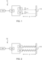
- an optical proximity sensor 10 relying on direct time-of-flight techniques may comprise a timing and control unit 100, an optical transmitter 102, an optical receiver 104 and optionally a human-machine interface 106.
- the timing and control unit 100 generates a control signal for the optical transmitter 102 which causes emission of an optical pulse from the optical transmitter, and at the same time t start triggers a timer internal to the timing and control unit 100.
- the optical pulse propagates towards a target object 110 and some of the backscattered light travels back to the optical receiver 104.
- An optical pulse being sensed at the receiver 104 causes the internal timer to stop at a certain time t stop .
- Mechanically scanning LIDAR devices (LIght Detection And Ranging) for use, e.g., in advanced driver assistance systems (ADAS) are exemplary of optical proximity sensors relying on direct time-of-flight techniques.
- a known optical proximity sensor 20 relying on frequency-domain reflectometry may comprise a timing and control unit 200, an optical transmitter 202, an optical receiver 204 and optionally a human-machine interface 206.
- the timing and control unit 200 generates a control signal for the optical emitter 202 which causes emission of an optical signal, whose intensity (amplitude) is modulated over time, from the optical transmitter 202.
- the known sensors relying on frequency-domain reflectometry are not suitable to provide low cost optical sensors insofar as they may involve complex systems, expensive electronics, accurate mechanical alignment between light emitter 202 and light detector 204, and temperature calibration.
- Sensors relying on light intensity evaluation may be affected by different light intensity environmental conditions and may involve a calibration phase and/or the implementation of calibrated look-up tables.
- Document US 2016/0320173 A1 discloses a method of measuring a change in an optical path length using differential laser self-mixing interferometry, and a corresponding measuring system.
- the method includes obtaining a reference self-mixing interferometric (SMI) signal and a main measurement SMI signal of a laser having a laser cavity, and determining the relative change in the optical path length between the laser and the target in a range between 0 and ⁇ /2, by comparing the relative positions along time of fringes or transitions of the main and reference SMI signals.
- SMI reference self-mixing interferometric
- the reference SMI signal and the main SMI signal are obtained at different moments once backscattered laser light is generated from the reflection on the target of a reference and a main measurement laser light beam emitted by the laser and while being modulated according to a specific modulation pattern that is maintained while both the reference SMI signal and the main SMI signal are acquired and has re-entered its laser cavity.
- low cost optical proximity sensors suitable for short-range distance measurements (e.g., with a range of approximately 0.5 m) are desirable.
- An object of one or more embodiments is to contribute in providing such improved solutions.
- such an object can be achieved by means of an optical proximity sensor having the features set forth in the claims that follow.
- One or more embodiments may relate to a corresponding method of operating the optical proximity sensor.
- One or more embodiments provide an optical proximity sensor comprising at least one solid-state device acting both as light emitter and as light detector.
- the solid-state device comprises at least one of an array of single photon avalanche diodes (SPADs), an array of avalanche photodiodes (APDs), or a silicon photomultiplier (SiPM).
- the optical proximity sensor comprises a driver circuit configured for biasing said emitter/detector device with a (periodically) modulated signal to cause emission of a modulated optical signal (e.g., having an intensity which varies over time).
- a modulated optical signal e.g., having an intensity which varies over time
- the driver circuit may be (fully) integrated within the optical proximity sensor to provide a so-called “single-chip” device.
- the driver circuit may be implemented on a different chip and coupled to the emitter/detector device.
- the optical parts of the sensor may be (fully) integrated within the optical proximity sensor, e.g., by process integration.
- the optical parts of the sensor may be discrete components.
- One or more embodiments may thus facilitate providing low cost optical proximity sensors for short-range measurements with improved accuracy.
- references to "an embodiment” or “one embodiment” in the framework of the present description is intended to indicate that a particular configuration, structure, or characteristic described in relation to the embodiment is comprised in at least one embodiment.
- phrases such as “in an embodiment” or “in one embodiment” that may be present in one or more points of the present description do not necessarily refer to one and the same embodiment.
- particular conformations, structures, or characteristics may be combined in any adequate way in one or more embodiments.
- FIG. 3 is a schematic block diagram exemplary of an optical proximity sensor 30 according to one or more embodiments.
- the sensor 30 comprises a solid-state device 300 configured to operate both as a light emitter and as a light detector (a photo-electric converter device).
- the emitter/detector device 300 comprises an array of single photon avalanche diodes (SPADs) or avalanche photodiodes (APDs), or a silicon photomultiplier (SiPM).
- the array may comprise between 100 and 10000 SPADs or APDs.
- the emitter/detector device 300 may comprise optical components such as lenses, coatings and layers with peculiar optical properties, which will be further described in the following.
- the sensor 30 comprises a driver circuit 302 configured for driving the emitter/detector device 300.
- the driver circuit 302 may comprise a modulation circuit configured for biasing the emitter/detector device 300 with a modulated signal, e.g., a periodic signal having a certain modulation frequency (for instance, in the range of 100 MHz to 3 GHz).
- the driver circuit 302 may be integrated on the same chip of the emitter/detector device 300, or may be implemented on a different chip and coupled to the emitter/detector device 300.
- the sensor 30 may comprise a signal conditioning circuit 304 configured for receiving an output signal indicative of light intensity from the emitter/detector device 300 and conditioning said output signal, e.g., for subsequent processing in a digital or analog processing circuit.
- the signal conditioning circuit 304 may comprise an (analog) amplification stage, an analog-to-digital converter (ADC) and a logic interface to a processing circuit.
- ADC analog-to-digital converter
- the signal conditioning circuit 304 may be integrated on the same chip of the emitter/detector device 300, or may be implemented on a different chip and coupled to the emitter/detector device 300.
- the sensor 30 may comprise a timing and control unit 306 configured for generating one or more control signal(s) for the operation of the driver circuit 302, and/or for processing one or more conditioned signals received from the signal conditioning circuit 304.
- the timing and control unit 306 may thus be configured to control operation of the whole sensor 30.
- the timing and control unit 306 may comprise a microcontroller circuit (MCU).
- one or more embodiments may comprise a device 300 configured to operate both as a light emitter and as a light detector, which may advantageously result in reduced cost and/or complexity of the sensor 30.
- the emitter/detector device 300 comprises an array of SPADs or APDs, or a SiPM, biased with a reverse-bias voltage (well) above the breakdown voltage, which is notionally employed as a photodetector device.
- the SPADs or APDs in the array may randomly generate avalanche events at a certain rate.
- an avalanche event taking place in a SPAD or APD may in turn result in emission of one or more photons from that SPAD or APD, i.e., an avalanche process in silicon may result in light emission.
- an avalanche process in silicon may result in light emission.
- about three photons may be emitted every 10 5 carriers generated in the SPAD or APD.
- a SiPM may be operated with a certain gain factor, e.g., about 5 ⁇ 10 6 , approximately 150 photons may be emitted on average by each SPAD or APD during an avalanche process.
- an array of SPADs or APDs, or a SiPM which is biased with a reverse-bias voltage above the breakdown voltage emits light with a certain intensity which may be a function of the biasing condition, insofar as the array of SPADs or APDs, or the SiPM, may comprise a high number of individual cells (e.g., hundreds or thousands of SPADs or APDs) so that, statistically, avalanche events happen at a constant rate even in absence of illumination, due to thermal generation of charge carriers.
- the light emitted from the array of SPADs or APDs, or the SiPM due to thermal generation effects (which in turn may cause avalanche effects, which in turn may result in light emission) may be modulated over time (e.g., at a certain frequency) by modulating the biasing condition of the array of SPADs or APDs, or the SiPM.
- the biasing voltage of the array of SPADs or APDs, or the SiPM may be (e.g., periodically) switched between a first value higher than the breakdown voltage and a second value lower than the breakdown voltage. Since light emission from the array of SPADs or APDs takes place (only) when the biasing voltage is above the breakdown voltage, such a biasing modulation scheme may result in emission of a (e.g., periodically) modulated optical signal (a sort of ON/OFF modulation), with such emitted optical signal being received at the same array of SPADs or APDs, which may also operate as a light detector, after reflection at a target object.
- a modulated optical signal a sort of ON/OFF modulation
- the biasing voltage of the array of SPADs or APDs, or the SiPM may be modulated between two values which are both higher than the breakdown voltage, but different from each other, thereby resulting in modulation of the intensity of a continuous optical signal.
- a modulation frequency of 300 MHz may result in a range of the sensor of approximately 0.5 m
- a modulation frequency of 1 GHz may result in a range of the sensor of approximately 0.15 m.
- the modulation frequency f m may be selected in the range of 100 MHz to 3 GHz.
- the modulation frequency f m may be selected as a trade-off between a target distance accuracy and a target distance range of the sensor.
- APDs, SPADs and/or SiPMs may have good timing jitter performances (e.g., a few tens of picoseconds) which however may not be sufficient to provide distance accuracy at the millimeter scale for an optical proximity sensor 30.
- Figure 3 is exemplary of an embodiment wherein the emitter/detector device 300, the driver circuit 302, the signal conditioning circuit 304 and the timing and control unit 306 are implemented on different chips.
- the emitter/detector device 300 and the driver circuit 302 may be implemented on the same chip 34.
- the emitter/detector device 300 and the signal conditioning circuit 304 may be implemented on the same chip 35.
- the emitter/detector device 300, the driver circuit 302 and the signal conditioning circuit 304 may be implemented on the same chip 36.
- the emitter/detector device 300 may comprise a plurality of light emitters/detectors 3007, e.g., a plurality of arrays of APDs or SPADs or a plurality of SiPMs. Providing a plurality of light emitters/detectors 3007 may facilitate executing a plurality M of measurements at the same time.
- the emitter/detector device 300 may comprise a reference channel 3008.
- a reference channel 3008 may be integrated (in a similar way as the plurality of arrays) in a single chip within the main device 30.
- a reference channel 3008 may be useful for evaluating background light.
- the emitter/detector device 300 may be placed in a case to avoid background illumination.
- the emitter/detector device 300 may comprise the following components/layers, which may be, for instance, discrete components:
- the optical components of the emitter/detector device 300 may be integrated by process integration.
- the emitter/detector device 300 may comprise a substrate 1000, an array of APDs or SPADs, or SiPM 1001, and a respective array of microlenses 1002 with integrated anti-reflection coating and background light (attenuation) filter.
- a metal layer (e.g., a tungsten layer) may be provided between adjacent APD or SPAD cells to avoid optical cross talk.
Landscapes
- Engineering & Computer Science (AREA)
- Physics & Mathematics (AREA)
- General Physics & Mathematics (AREA)
- Computer Networks & Wireless Communication (AREA)
- Radar, Positioning & Navigation (AREA)
- Remote Sensing (AREA)
- Electromagnetism (AREA)
- Life Sciences & Earth Sciences (AREA)
- Sustainable Development (AREA)
- Spectroscopy & Molecular Physics (AREA)
- Optical Radar Systems And Details Thereof (AREA)
- Measurement Of Optical Distance (AREA)
- Switches Operated By Changes In Physical Conditions (AREA)
- Electrophonic Musical Instruments (AREA)
Claims (11)
- Optischer Näherungssensor (30), umfassend einen photoelektrischen Festkörperwandler (300), eine Vorspannungsschaltung (302) zum Vorspannen des photoelektrischen Festkörperwandlers und eine Antriebsschaltung (306), wobei der photoelektrische Festkörperwandler (300) mindestens eines von Folgendem umfasst:Ein Array von Einzelphotonen-Avalanche-Dioden,ein Array von Avalanche-Photodioden, undeinem Silizium-Fotomultiplier,und wobei die Antriebsschaltung (306) konfiguriert ist, um:Die Vorspannungsschaltung (302) zu steuern, um an den photoelektrischen Festkörperwandler (300) ein Vorspannungssignal anzulegen, das zwischen einem ersten Wert und einem zweiten Wert moduliert ist, wobei sich der zweite Wert von dem ersten Wert unterscheidet, wobei der erste Wert des Vorspannungssignals höher ist als eine Durchbruchspannung des photoelektrischen Festkörperwandlers (300), und wobei ein moduliertes optisches Signal von dem photoelektrischen Festkörperwandler (300) in Richtung eines Zielobjekts ausgestrahlt wird,ein elektrisches Ausgangssignal von dem photoelektrischen Festkörperwandler (300) zu empfangen (304), wobei das elektrische Ausgangssignal in Abhängigkeit von einem modulierten optischen Signal ist, das an dem photoelektrischen Festkörperwandler (300) als Ergebnis der Reflexion des ausgestrahlten modulierten optischen Signals an dem Zielobjekt empfangen wird,einen Phasenvergleich des an den photoelektrischen Wandler (300) angelegten modulierten Vorspannungssignals mit dem von dem photoelektrischen Festkörperwandler (300) empfangenen elektrischen Ausgangssignal durchzuführen und als Ergebnis des Phasenvergleichs ein Phasenverschiebungssignal zu erzeugen, das eine Funktion der Phasenverschiebung zwischen dem von dem photoelektrischen Festkörperwandler (300) ausgestrahlten modulierten optischen Signal und dem an dem photoelektrischen Festkörperwandler (300) empfangenen modulierten optischen Signal ist, undeinen Abstand zwischen dem optischen Näherungssensor (30) und dem Zielobjekt in Abhängigkeit von dem Phasenverschiebungssignal zu berechnen.
- Optischer Näherungssensor (30) nach Anspruch 1, wobei die Vorspannungsschaltung (302) eine Modulationsschaltung umfasst, die so konfiguriert ist, dass sie das Vorspannungssignal periodisch zwischen dem ersten Wert und dem zweiten Wert mit einer Frequenz von 100 MHz bis 3 GHz moduliert, wobei ein optisches Signal, das periodisch mit einer Frequenz von 100 MHz bis 3 GHz moduliert wird, von dem photoelektrischen Festkörperwandler (300) ausgestrahlt wird.
- Optischer Näherungssensor (30) nach Anspruch 1 oder 2, wobei der zweite Wert des Vorspannungssignals niedriger ist als die Durchbruchspannung des photoelektrischen Festkörperwandlers (300).
- Optischer Näherungssensor (30) nach Anspruch 1 oder 2, wobei der zweite Wert des Vorspannungssignals höher ist als die Durchbruchspannung des photoelektrischen Festkörperwandlers (300).
- Optischer Näherungssensor (30) nach einem der vorstehenden Ansprüche, umfassend eine Konditionierungsschaltung (304), die so konfiguriert ist, dass sie das elektrische Ausgangssignal des photoelektrischen Festkörperwandlers (300) konditioniert und ein konditioniertes elektrisches Signal für die Antriebsschaltung (306) bereitstellt.
- Optischer Näherungssensor (30) nach Anspruch 5, wobei mindestens zwei von dem photoelektrischen Festkörperwandler (300), der Vorspannungsschaltung (302) und der Konditionierungsschaltung (304) auf demselben Halbleiterchip (34; 35; 36) implementiert sind.
- Optischer Näherungssensor (30) nach einem der vorstehenden Ansprüche, wobei der photoelektrische Festkörperwandler (300) Folgendes umfasst:Eine Antireflexionsbeschichtung (902),einen Hintergrundlichtabschwächungsfilter (903) undeine Linse (904).
- Optischer Näherungssensor (30) nach einem der vorstehenden Ansprüche, wobei der photoelektrische Festkörperwandler (300) ein entsprechendes Array von Linsen (1002) umfasst, wobei die Linsen in dem Array von Linsen eine Antireflexionsbeschichtung und einen Filter zur Abschwächung des Hintergrundlichts aufweisen, der darin integriert ist.
- Optischer Näherungssensor (30) nach einem der vorstehenden Ansprüche, wobei der photoelektrische Festkörperwandler (300) einen Referenzkanal (3008) umfasst, der so konfiguriert ist, dass er ein Hintergrundlicht auswertet.
- Optischer Näherungssensor (30) nach einem der vorstehenden Ansprüche, wobei die Antriebsschaltung (306) konfiguriert ist, um:Eine Vielzahl von Phasenvergleichen des modulierten Vorspannungssignals, das an den photoelektrischen Wandler (300) angelegt wird, mit dem vom photoelektrischen Festkörperwandler (300) empfangenen elektrischen Ausgangssignal durchzuführen und eine entsprechende Vielzahl von Werten des Phasenverschiebungssignals zu erzeugen, undeinen Abstand zwischen dem optischen Näherungssensor (30) und dem Zielobjekt in Abhängigkeit von der Vielzahl von Werten des Phasenverschiebungssignals zu berechnen.
- Verfahren zum Betreiben eines optischen Näherungssensors (30) nach einem der vorstehenden Ansprüche, das Verfahren umfassend:Anlegen eines Vorspannungssignals an den photoelektrischen Festkörperwandler (300), das zwischen einem ersten Wert und einem zweiten Wert moduliert ist, wobei sich der zweite Wert von dem ersten Wert unterscheidet, wobei der erste Wert des Vorspannungssignals höher ist als eine Durchbruchspannung des photoelektrischen Festkörperwandlers (300), und wobei ein moduliertes optisches Signal von dem photoelektrischen Festkörperwandler (300) in Richtung eines Zielobjekts ausgestrahlt wird,Empfangen (304) eines elektrischen Ausgangssignals von dem photoelektrischen Festkörperwandler (300), wobei das elektrische Ausgangssignal in Abhängigkeit von einem modulierten optischen Signal ist, das an dem photoelektrischen Festkörperwandler (300) als Ergebnis der Reflexion des ausgestrahlten modulierten optischen Signals an dem Zielobjekt empfangen wird,Durchführen eines Phasenvergleichs des modulierten Vorspannungssignals, das an den photoelektrischen Wandler (300) angelegt wird, mit dem elektrischen Ausgabesignal, das von dem photoelektrischen Festkörperwandler (300) empfangen wird,Erzeugen eines Phasenverschiebungssignals in Abhängigkeit von der Phasenverschiebung zwischen dem von dem photoelektrischen Festkörperwandler (300) ausgestrahlten modulierten optischen Signal und dem an dem photoelektrischen Festkörperwandler (300) empfangenen modulierten optischen Signal als Ergebnis des Phasenvergleichs, undBerechnen eines Abstands zwischen dem optischen Näherungssensor (30) und dem Zielobjekt in Abhängigkeit von dem Phasenverschiebungssignal.
Applications Claiming Priority (1)
| Application Number | Priority Date | Filing Date | Title |
|---|---|---|---|
| IT102019000015761A IT201900015761A1 (it) | 2019-09-06 | 2019-09-06 | Sensore ottico di prossimità e corrispondente procedimento di funzionamento |
Publications (2)
| Publication Number | Publication Date |
|---|---|
| EP3789793A1 EP3789793A1 (de) | 2021-03-10 |
| EP3789793B1 true EP3789793B1 (de) | 2023-07-19 |
Family
ID=69173244
Family Applications (1)
| Application Number | Title | Priority Date | Filing Date |
|---|---|---|---|
| EP20192064.2A Active EP3789793B1 (de) | 2019-09-06 | 2020-08-21 | Optischer näherungssensor und entsprechendes betriebsverfahren |
Country Status (4)
| Country | Link |
|---|---|
| US (1) | US12007482B2 (de) |
| EP (1) | EP3789793B1 (de) |
| CN (2) | CN112558093B (de) |
| IT (1) | IT201900015761A1 (de) |
Families Citing this family (5)
| Publication number | Priority date | Publication date | Assignee | Title |
|---|---|---|---|---|
| IT201900015761A1 (it) * | 2019-09-06 | 2021-03-06 | St Microelectronics Srl | Sensore ottico di prossimità e corrispondente procedimento di funzionamento |
| CA3099061A1 (en) * | 2019-11-15 | 2021-05-15 | Op-Hygiene Ip Gmbh | Fluid dispenser with wake up sensor |
| CN113748360A (zh) * | 2020-01-16 | 2021-12-03 | 索尼半导体解决方案公司 | 光源装置、光源装置的制造方法以及电子设备 |
| CN114935746A (zh) * | 2021-04-30 | 2022-08-23 | 深圳阜时科技有限公司 | 一种发光组件、发射模组、感测装置及电子设备 |
| CN118836905A (zh) * | 2024-06-24 | 2024-10-25 | 深圳市志奋领科技有限公司 | 一种背景抑制光电传感器 |
Family Cites Families (10)
| Publication number | Priority date | Publication date | Assignee | Title |
|---|---|---|---|---|
| US20050035361A1 (en) * | 2003-08-15 | 2005-02-17 | Peterson Charles M. | Polarized light emitting devices and methods |
| US7283214B2 (en) * | 2005-10-14 | 2007-10-16 | Microsoft Corporation | Self-mixing laser range sensor |
| EP2887008A1 (de) * | 2013-12-17 | 2015-06-24 | Universitat Politècnica de Catalunya | Verfahren zur Messung einer Änderung in einem optischen Pfad mit differenzieller selbstmischender Laser-Interferometrie sowie differenzielles selbstmischendes Laser-Interferometriemesssystem |
| CN107367790B (zh) * | 2014-02-24 | 2019-12-06 | 洛克利光子有限公司 | 检测器重调器和光电子交换机 |
| DE102014111431B4 (de) * | 2014-08-11 | 2024-07-11 | Infineon Technologies Ag | Flugzeitvorrichtungen |
| CN104851930B (zh) * | 2015-04-02 | 2017-07-25 | 西北工业大学 | 全固态光电转换器件及其制备方法 |
| US9823118B2 (en) * | 2015-12-26 | 2017-11-21 | Intel Corporation | Low power, high resolution solid state LIDAR circuit |
| WO2019123825A1 (ja) * | 2017-12-22 | 2019-06-27 | ソニーセミコンダクタソリューションズ株式会社 | 信号生成装置 |
| TWI845592B (zh) * | 2019-01-30 | 2024-06-21 | 日商索尼半導體解決方案公司 | 受光裝置及測距系統 |
| IT201900015761A1 (it) * | 2019-09-06 | 2021-03-06 | St Microelectronics Srl | Sensore ottico di prossimità e corrispondente procedimento di funzionamento |
-
2019
- 2019-09-06 IT IT102019000015761A patent/IT201900015761A1/it unknown
-
2020
- 2020-08-21 EP EP20192064.2A patent/EP3789793B1/de active Active
- 2020-09-03 US US17/011,867 patent/US12007482B2/en active Active
- 2020-09-07 CN CN202010927579.1A patent/CN112558093B/zh active Active
- 2020-09-07 CN CN202021927590.XU patent/CN212905460U/zh not_active Withdrawn - After Issue
Also Published As
| Publication number | Publication date |
|---|---|
| IT201900015761A1 (it) | 2021-03-06 |
| US20210072386A1 (en) | 2021-03-11 |
| EP3789793A1 (de) | 2021-03-10 |
| CN112558093B (zh) | 2025-07-15 |
| CN112558093A (zh) | 2021-03-26 |
| US12007482B2 (en) | 2024-06-11 |
| CN212905460U (zh) | 2021-04-06 |
Similar Documents
| Publication | Publication Date | Title |
|---|---|---|
| EP3789793B1 (de) | Optischer näherungssensor und entsprechendes betriebsverfahren | |
| US11022680B2 (en) | Distance measuring device with SPAD array and range walk compensenation | |
| US20240061091A1 (en) | Method for measuring reflectivity of target object by using lidar, and lidar | |
| CN110244311B (zh) | 激光雷达接收装置、激光雷达系统和激光测距方法 | |
| CN111983589B (zh) | 单光子雪崩二极管(spad)微单元阵列及其操作方法 | |
| US11725935B2 (en) | Distance meter comprising SPAD arrangement for consideration of multiple targets | |
| CN211014629U (zh) | 一种激光雷达装置 | |
| CN211014630U (zh) | 激光雷达设备及机动车系统 | |
| CN207557476U (zh) | 基于单光子探测技术的激光测距系统 | |
| JP2009524072A (ja) | 光伝搬時間の測定方法 | |
| WO2023103310A1 (zh) | 激光雷达及其测量目标反射率的方法和系统 | |
| CA3085648C (en) | Arrangement and method for determining a distance of at least one object using light signals | |
| US12044804B2 (en) | Range estimation for Lidar systems using a detector array | |
| CN108732578A (zh) | 测距仪系统及对其校准并确定到外部对象的距离的方法 | |
| US20220171038A1 (en) | Multichannel time-of-flight measurement device with time-to-digital converters in a programmable integrated circuit | |
| US12436286B2 (en) | LIDAR device and method of operating the same | |
| KR20220106646A (ko) | 직접 tof 측정 기반 거리 센서를 위한 가변 펄스 생성기 | |
| US20220155442A1 (en) | Light detection device, lidar device including the same, and method of measuring distance | |
| Golovkov et al. | Receiving system of a pulsed laser rangefinder | |
| CN118688815A (zh) | 一种基于正弦强度调制脉冲光源的激光测距系统 | |
| KR20220008734A (ko) | Fmcw 라이다를 위한 리드아웃 아키텍쳐 | |
| CN115508812A (zh) | 一种用于spad自校准的像素电路及其方法 | |
| Zhang et al. | Design and experiment of phase laser ranging system based on MEMS mirror for scanning detection | |
| US20250216519A1 (en) | High-range, low-power lidar systems, and related methods and apparatus | |
| CN121028107A (zh) | 光学测距方法及装置 |
Legal Events
| Date | Code | Title | Description |
|---|---|---|---|
| PUAI | Public reference made under article 153(3) epc to a published international application that has entered the european phase |
Free format text: ORIGINAL CODE: 0009012 |
|
| STAA | Information on the status of an ep patent application or granted ep patent |
Free format text: STATUS: THE APPLICATION HAS BEEN PUBLISHED |
|
| AK | Designated contracting states |
Kind code of ref document: A1 Designated state(s): AL AT BE BG CH CY CZ DE DK EE ES FI FR GB GR HR HU IE IS IT LI LT LU LV MC MK MT NL NO PL PT RO RS SE SI SK SM TR |
|
| AX | Request for extension of the european patent |
Extension state: BA ME |
|
| STAA | Information on the status of an ep patent application or granted ep patent |
Free format text: STATUS: REQUEST FOR EXAMINATION WAS MADE |
|
| 17P | Request for examination filed |
Effective date: 20210803 |
|
| RBV | Designated contracting states (corrected) |
Designated state(s): AL AT BE BG CH CY CZ DE DK EE ES FI FR GB GR HR HU IE IS IT LI LT LU LV MC MK MT NL NO PL PT RO RS SE SI SK SM TR |
|
| GRAP | Despatch of communication of intention to grant a patent |
Free format text: ORIGINAL CODE: EPIDOSNIGR1 |
|
| STAA | Information on the status of an ep patent application or granted ep patent |
Free format text: STATUS: GRANT OF PATENT IS INTENDED |
|
| INTG | Intention to grant announced |
Effective date: 20230322 |
|
| GRAS | Grant fee paid |
Free format text: ORIGINAL CODE: EPIDOSNIGR3 |
|
| GRAA | (expected) grant |
Free format text: ORIGINAL CODE: 0009210 |
|
| STAA | Information on the status of an ep patent application or granted ep patent |
Free format text: STATUS: THE PATENT HAS BEEN GRANTED |
|
| AK | Designated contracting states |
Kind code of ref document: B1 Designated state(s): AL AT BE BG CH CY CZ DE DK EE ES FI FR GB GR HR HU IE IS IT LI LT LU LV MC MK MT NL NO PL PT RO RS SE SI SK SM TR |
|
| REG | Reference to a national code |
Ref country code: GB Ref legal event code: FG4D |
|
| REG | Reference to a national code |
Ref country code: CH Ref legal event code: EP |
|
| REG | Reference to a national code |
Ref country code: DE Ref legal event code: R096 Ref document number: 602020013967 Country of ref document: DE |
|
| REG | Reference to a national code |
Ref country code: IE Ref legal event code: FG4D |
|
| REG | Reference to a national code |
Ref country code: LT Ref legal event code: MG9D |
|
| REG | Reference to a national code |
Ref country code: NL Ref legal event code: MP Effective date: 20230719 |
|
| REG | Reference to a national code |
Ref country code: AT Ref legal event code: MK05 Ref document number: 1590003 Country of ref document: AT Kind code of ref document: T Effective date: 20230719 |
|
| PG25 | Lapsed in a contracting state [announced via postgrant information from national office to epo] |
Ref country code: NL Free format text: LAPSE BECAUSE OF FAILURE TO SUBMIT A TRANSLATION OF THE DESCRIPTION OR TO PAY THE FEE WITHIN THE PRESCRIBED TIME-LIMIT Effective date: 20230719 |
|
| PG25 | Lapsed in a contracting state [announced via postgrant information from national office to epo] |
Ref country code: GR Free format text: LAPSE BECAUSE OF FAILURE TO SUBMIT A TRANSLATION OF THE DESCRIPTION OR TO PAY THE FEE WITHIN THE PRESCRIBED TIME-LIMIT Effective date: 20231020 |
|
| PG25 | Lapsed in a contracting state [announced via postgrant information from national office to epo] |
Ref country code: IS Free format text: LAPSE BECAUSE OF FAILURE TO SUBMIT A TRANSLATION OF THE DESCRIPTION OR TO PAY THE FEE WITHIN THE PRESCRIBED TIME-LIMIT Effective date: 20231119 |
|
| PG25 | Lapsed in a contracting state [announced via postgrant information from national office to epo] |
Ref country code: SE Free format text: LAPSE BECAUSE OF FAILURE TO SUBMIT A TRANSLATION OF THE DESCRIPTION OR TO PAY THE FEE WITHIN THE PRESCRIBED TIME-LIMIT Effective date: 20230719 Ref country code: RS Free format text: LAPSE BECAUSE OF FAILURE TO SUBMIT A TRANSLATION OF THE DESCRIPTION OR TO PAY THE FEE WITHIN THE PRESCRIBED TIME-LIMIT Effective date: 20230719 Ref country code: PT Free format text: LAPSE BECAUSE OF FAILURE TO SUBMIT A TRANSLATION OF THE DESCRIPTION OR TO PAY THE FEE WITHIN THE PRESCRIBED TIME-LIMIT Effective date: 20231120 Ref country code: NO Free format text: LAPSE BECAUSE OF FAILURE TO SUBMIT A TRANSLATION OF THE DESCRIPTION OR TO PAY THE FEE WITHIN THE PRESCRIBED TIME-LIMIT Effective date: 20231019 Ref country code: LV Free format text: LAPSE BECAUSE OF FAILURE TO SUBMIT A TRANSLATION OF THE DESCRIPTION OR TO PAY THE FEE WITHIN THE PRESCRIBED TIME-LIMIT Effective date: 20230719 Ref country code: LT Free format text: LAPSE BECAUSE OF FAILURE TO SUBMIT A TRANSLATION OF THE DESCRIPTION OR TO PAY THE FEE WITHIN THE PRESCRIBED TIME-LIMIT Effective date: 20230719 Ref country code: IS Free format text: LAPSE BECAUSE OF FAILURE TO SUBMIT A TRANSLATION OF THE DESCRIPTION OR TO PAY THE FEE WITHIN THE PRESCRIBED TIME-LIMIT Effective date: 20231119 Ref country code: HR Free format text: LAPSE BECAUSE OF FAILURE TO SUBMIT A TRANSLATION OF THE DESCRIPTION OR TO PAY THE FEE WITHIN THE PRESCRIBED TIME-LIMIT Effective date: 20230719 Ref country code: GR Free format text: LAPSE BECAUSE OF FAILURE TO SUBMIT A TRANSLATION OF THE DESCRIPTION OR TO PAY THE FEE WITHIN THE PRESCRIBED TIME-LIMIT Effective date: 20231020 Ref country code: FI Free format text: LAPSE BECAUSE OF FAILURE TO SUBMIT A TRANSLATION OF THE DESCRIPTION OR TO PAY THE FEE WITHIN THE PRESCRIBED TIME-LIMIT Effective date: 20230719 Ref country code: AT Free format text: LAPSE BECAUSE OF FAILURE TO SUBMIT A TRANSLATION OF THE DESCRIPTION OR TO PAY THE FEE WITHIN THE PRESCRIBED TIME-LIMIT Effective date: 20230719 |
|
| PG25 | Lapsed in a contracting state [announced via postgrant information from national office to epo] |
Ref country code: PL Free format text: LAPSE BECAUSE OF FAILURE TO SUBMIT A TRANSLATION OF THE DESCRIPTION OR TO PAY THE FEE WITHIN THE PRESCRIBED TIME-LIMIT Effective date: 20230719 |
|
| REG | Reference to a national code |
Ref country code: CH Ref legal event code: PL |
|
| PG25 | Lapsed in a contracting state [announced via postgrant information from national office to epo] |
Ref country code: LU Free format text: LAPSE BECAUSE OF NON-PAYMENT OF DUE FEES Effective date: 20230821 |
|
| REG | Reference to a national code |
Ref country code: DE Ref legal event code: R097 Ref document number: 602020013967 Country of ref document: DE |
|
| PG25 | Lapsed in a contracting state [announced via postgrant information from national office to epo] |
Ref country code: ES Free format text: LAPSE BECAUSE OF FAILURE TO SUBMIT A TRANSLATION OF THE DESCRIPTION OR TO PAY THE FEE WITHIN THE PRESCRIBED TIME-LIMIT Effective date: 20230719 |
|
| PG25 | Lapsed in a contracting state [announced via postgrant information from national office to epo] |
Ref country code: SM Free format text: LAPSE BECAUSE OF FAILURE TO SUBMIT A TRANSLATION OF THE DESCRIPTION OR TO PAY THE FEE WITHIN THE PRESCRIBED TIME-LIMIT Effective date: 20230719 Ref country code: RO Free format text: LAPSE BECAUSE OF FAILURE TO SUBMIT A TRANSLATION OF THE DESCRIPTION OR TO PAY THE FEE WITHIN THE PRESCRIBED TIME-LIMIT Effective date: 20230719 Ref country code: LU Free format text: LAPSE BECAUSE OF NON-PAYMENT OF DUE FEES Effective date: 20230821 Ref country code: ES Free format text: LAPSE BECAUSE OF FAILURE TO SUBMIT A TRANSLATION OF THE DESCRIPTION OR TO PAY THE FEE WITHIN THE PRESCRIBED TIME-LIMIT Effective date: 20230719 Ref country code: EE Free format text: LAPSE BECAUSE OF FAILURE TO SUBMIT A TRANSLATION OF THE DESCRIPTION OR TO PAY THE FEE WITHIN THE PRESCRIBED TIME-LIMIT Effective date: 20230719 Ref country code: DK Free format text: LAPSE BECAUSE OF FAILURE TO SUBMIT A TRANSLATION OF THE DESCRIPTION OR TO PAY THE FEE WITHIN THE PRESCRIBED TIME-LIMIT Effective date: 20230719 Ref country code: CZ Free format text: LAPSE BECAUSE OF FAILURE TO SUBMIT A TRANSLATION OF THE DESCRIPTION OR TO PAY THE FEE WITHIN THE PRESCRIBED TIME-LIMIT Effective date: 20230719 Ref country code: SK Free format text: LAPSE BECAUSE OF FAILURE TO SUBMIT A TRANSLATION OF THE DESCRIPTION OR TO PAY THE FEE WITHIN THE PRESCRIBED TIME-LIMIT Effective date: 20230719 Ref country code: MC Free format text: LAPSE BECAUSE OF FAILURE TO SUBMIT A TRANSLATION OF THE DESCRIPTION OR TO PAY THE FEE WITHIN THE PRESCRIBED TIME-LIMIT Effective date: 20230719 Ref country code: CH Free format text: LAPSE BECAUSE OF NON-PAYMENT OF DUE FEES Effective date: 20230831 |
|
| REG | Reference to a national code |
Ref country code: BE Ref legal event code: MM Effective date: 20230831 |
|
| REG | Reference to a national code |
Ref country code: IE Ref legal event code: MM4A |
|
| PLBE | No opposition filed within time limit |
Free format text: ORIGINAL CODE: 0009261 |
|
| STAA | Information on the status of an ep patent application or granted ep patent |
Free format text: STATUS: NO OPPOSITION FILED WITHIN TIME LIMIT |
|
| PG25 | Lapsed in a contracting state [announced via postgrant information from national office to epo] |
Ref country code: IT Free format text: LAPSE BECAUSE OF FAILURE TO SUBMIT A TRANSLATION OF THE DESCRIPTION OR TO PAY THE FEE WITHIN THE PRESCRIBED TIME-LIMIT Effective date: 20230719 |
|
| 26N | No opposition filed |
Effective date: 20240422 |
|
| PG25 | Lapsed in a contracting state [announced via postgrant information from national office to epo] |
Ref country code: IE Free format text: LAPSE BECAUSE OF NON-PAYMENT OF DUE FEES Effective date: 20230821 |
|
| PG25 | Lapsed in a contracting state [announced via postgrant information from national office to epo] |
Ref country code: IE Free format text: LAPSE BECAUSE OF NON-PAYMENT OF DUE FEES Effective date: 20230821 Ref country code: FR Free format text: LAPSE BECAUSE OF NON-PAYMENT OF DUE FEES Effective date: 20230919 Ref country code: SI Free format text: LAPSE BECAUSE OF FAILURE TO SUBMIT A TRANSLATION OF THE DESCRIPTION OR TO PAY THE FEE WITHIN THE PRESCRIBED TIME-LIMIT Effective date: 20230719 |
|
| PG25 | Lapsed in a contracting state [announced via postgrant information from national office to epo] |
Ref country code: BE Free format text: LAPSE BECAUSE OF NON-PAYMENT OF DUE FEES Effective date: 20230831 |
|
| PG25 | Lapsed in a contracting state [announced via postgrant information from national office to epo] |
Ref country code: BG Free format text: LAPSE BECAUSE OF FAILURE TO SUBMIT A TRANSLATION OF THE DESCRIPTION OR TO PAY THE FEE WITHIN THE PRESCRIBED TIME-LIMIT Effective date: 20230719 |
|
| PG25 | Lapsed in a contracting state [announced via postgrant information from national office to epo] |
Ref country code: BG Free format text: LAPSE BECAUSE OF FAILURE TO SUBMIT A TRANSLATION OF THE DESCRIPTION OR TO PAY THE FEE WITHIN THE PRESCRIBED TIME-LIMIT Effective date: 20230719 |
|
| GBPC | Gb: european patent ceased through non-payment of renewal fee |
Effective date: 20240821 |
|
| PG25 | Lapsed in a contracting state [announced via postgrant information from national office to epo] |
Ref country code: GB Free format text: LAPSE BECAUSE OF NON-PAYMENT OF DUE FEES Effective date: 20240821 |
|
| PG25 | Lapsed in a contracting state [announced via postgrant information from national office to epo] |
Ref country code: CY Free format text: LAPSE BECAUSE OF FAILURE TO SUBMIT A TRANSLATION OF THE DESCRIPTION OR TO PAY THE FEE WITHIN THE PRESCRIBED TIME-LIMIT; INVALID AB INITIO Effective date: 20200821 |
|
| PG25 | Lapsed in a contracting state [announced via postgrant information from national office to epo] |
Ref country code: HU Free format text: LAPSE BECAUSE OF FAILURE TO SUBMIT A TRANSLATION OF THE DESCRIPTION OR TO PAY THE FEE WITHIN THE PRESCRIBED TIME-LIMIT; INVALID AB INITIO Effective date: 20200821 |
|
| PGFP | Annual fee paid to national office [announced via postgrant information from national office to epo] |
Ref country code: DE Payment date: 20250724 Year of fee payment: 6 |
|
| PG25 | Lapsed in a contracting state [announced via postgrant information from national office to epo] |
Ref country code: TR Free format text: LAPSE BECAUSE OF FAILURE TO SUBMIT A TRANSLATION OF THE DESCRIPTION OR TO PAY THE FEE WITHIN THE PRESCRIBED TIME-LIMIT Effective date: 20230719 |