EP3789855A1 - Taststiftspitzenentwurf und genauigkeitsverbesserung - Google Patents
Taststiftspitzenentwurf und genauigkeitsverbesserung Download PDFInfo
- Publication number
- EP3789855A1 EP3789855A1 EP19195507.9A EP19195507A EP3789855A1 EP 3789855 A1 EP3789855 A1 EP 3789855A1 EP 19195507 A EP19195507 A EP 19195507A EP 3789855 A1 EP3789855 A1 EP 3789855A1
- Authority
- EP
- European Patent Office
- Prior art keywords
- stylus
- tip
- nib
- electrode
- nib portion
- Prior art date
- Legal status (The legal status is an assumption and is not a legal conclusion. Google has not performed a legal analysis and makes no representation as to the accuracy of the status listed.)
- Withdrawn
Links
Images




Classifications
-
- G—PHYSICS
- G06—COMPUTING OR CALCULATING; COUNTING
- G06F—ELECTRIC DIGITAL DATA PROCESSING
- G06F3/00—Input arrangements for transferring data to be processed into a form capable of being handled by the computer; Output arrangements for transferring data from processing unit to output unit, e.g. interface arrangements
- G06F3/01—Input arrangements or combined input and output arrangements for interaction between user and computer
- G06F3/03—Arrangements for converting the position or the displacement of a member into a coded form
- G06F3/033—Pointing devices displaced or positioned by the user, e.g. mice, trackballs, pens or joysticks; Accessories therefor
- G06F3/0354—Pointing devices displaced or positioned by the user, e.g. mice, trackballs, pens or joysticks; Accessories therefor with detection of two-dimensional [2D] relative movements between the device, or an operating part thereof, and a plane or surface, e.g. 2D mice, trackballs, pens or pucks
- G06F3/03545—Pens or stylus
-
- G—PHYSICS
- G06—COMPUTING OR CALCULATING; COUNTING
- G06F—ELECTRIC DIGITAL DATA PROCESSING
- G06F3/00—Input arrangements for transferring data to be processed into a form capable of being handled by the computer; Output arrangements for transferring data from processing unit to output unit, e.g. interface arrangements
- G06F3/01—Input arrangements or combined input and output arrangements for interaction between user and computer
- G06F3/03—Arrangements for converting the position or the displacement of a member into a coded form
- G06F3/033—Pointing devices displaced or positioned by the user, e.g. mice, trackballs, pens or joysticks; Accessories therefor
- G06F3/0354—Pointing devices displaced or positioned by the user, e.g. mice, trackballs, pens or joysticks; Accessories therefor with detection of two-dimensional [2D] relative movements between the device, or an operating part thereof, and a plane or surface, e.g. 2D mice, trackballs, pens or pucks
- G06F3/03545—Pens or stylus
- G06F3/03546—Pens or stylus using a rotatable ball at the tip as position detecting member
-
- G—PHYSICS
- G06—COMPUTING OR CALCULATING; COUNTING
- G06F—ELECTRIC DIGITAL DATA PROCESSING
- G06F3/00—Input arrangements for transferring data to be processed into a form capable of being handled by the computer; Output arrangements for transferring data from processing unit to output unit, e.g. interface arrangements
- G06F3/01—Input arrangements or combined input and output arrangements for interaction between user and computer
- G06F3/03—Arrangements for converting the position or the displacement of a member into a coded form
- G06F3/033—Pointing devices displaced or positioned by the user, e.g. mice, trackballs, pens or joysticks; Accessories therefor
- G06F3/038—Control and interface arrangements therefor, e.g. drivers or device-embedded control circuitry
- G06F3/0383—Signal control means within the pointing device
-
- G—PHYSICS
- G06—COMPUTING OR CALCULATING; COUNTING
- G06F—ELECTRIC DIGITAL DATA PROCESSING
- G06F3/00—Input arrangements for transferring data to be processed into a form capable of being handled by the computer; Output arrangements for transferring data from processing unit to output unit, e.g. interface arrangements
- G06F3/01—Input arrangements or combined input and output arrangements for interaction between user and computer
- G06F3/03—Arrangements for converting the position or the displacement of a member into a coded form
- G06F3/041—Digitisers, e.g. for touch screens or touch pads, characterised by the transducing means
- G06F3/0416—Control or interface arrangements specially adapted for digitisers
- G06F3/04162—Control or interface arrangements specially adapted for digitisers for exchanging data with external devices, e.g. smart pens, via the digitiser sensing hardware
-
- G—PHYSICS
- G06—COMPUTING OR CALCULATING; COUNTING
- G06F—ELECTRIC DIGITAL DATA PROCESSING
- G06F3/00—Input arrangements for transferring data to be processed into a form capable of being handled by the computer; Output arrangements for transferring data from processing unit to output unit, e.g. interface arrangements
- G06F3/01—Input arrangements or combined input and output arrangements for interaction between user and computer
- G06F3/03—Arrangements for converting the position or the displacement of a member into a coded form
- G06F3/041—Digitisers, e.g. for touch screens or touch pads, characterised by the transducing means
- G06F3/044—Digitisers, e.g. for touch screens or touch pads, characterised by the transducing means by capacitive means
- G06F3/0441—Digitisers, e.g. for touch screens or touch pads, characterised by the transducing means by capacitive means using active external devices, e.g. active pens, for receiving changes in electrical potential transmitted by the digitiser, e.g. tablet driving signals
-
- G—PHYSICS
- G06—COMPUTING OR CALCULATING; COUNTING
- G06F—ELECTRIC DIGITAL DATA PROCESSING
- G06F3/00—Input arrangements for transferring data to be processed into a form capable of being handled by the computer; Output arrangements for transferring data from processing unit to output unit, e.g. interface arrangements
- G06F3/01—Input arrangements or combined input and output arrangements for interaction between user and computer
- G06F3/03—Arrangements for converting the position or the displacement of a member into a coded form
- G06F3/041—Digitisers, e.g. for touch screens or touch pads, characterised by the transducing means
- G06F3/044—Digitisers, e.g. for touch screens or touch pads, characterised by the transducing means by capacitive means
- G06F3/0442—Digitisers, e.g. for touch screens or touch pads, characterised by the transducing means by capacitive means using active external devices, e.g. active pens, for transmitting changes in electrical potential to be received by the digitiser
Definitions
- the touch-sensitive display device may detect a touch event each time the stylus touches or comes into close proximity with a touch sensor of the touch-sensitive display device.
- a touch event may be interpreted by the touch-sensitive display device as a user input at a particular two- or three-dimensional location relative to the touch-sensitive display device.
- the outer diameter of the ring electrode 12 may range between 1mm and 15mm, while the size of the tip electrode 14 should not exceed the outer diameter of the ring electrode 12.
- the nib portion 10 Due to the molded design of the nib portion 10, a constant and fixed gap can be kept between the tip and ring electrodes 14, 12. Furthermore, the height of the tip and ring electrodes 14, 12 can be well controlled on the design level and during production. Moreover, the diameter of the ring electrode 12 can be made very flexible, as it is no longer limited by the size of the housing 20 of the active stylus. Also, the tail portion 16 of the nib portion 10 towards the housing 20 can be made narrow and may be covered by the ring electrode 12, so that the generation of an extra tail can be prevented. In general, the nib portion 10 with the integrated tip and ring electrodes 14, 12 can be molded in any desirable shape as required by an intended implementation.
- FIG 2 is a schematic block diagram of a signal processing portion in an example of an active stylus with removable single-unit (e.g. molded) nib portion 10.
- the active stylus is usable with a touch-sensitive display device (not shown in Figure 2 ) incorporating a touch sensor, wherein interactions between the tip and ring electrodes 14, 12 of the single-unit nib portion 10 and the touch matrix result in control logic of the touch-sensitive display device receiving spatial capacitance measurements.
- the controller 210 may also be connected to a conductive layer or casing 200 of the housing 20 of the active stylus in order to use the conductive layer or casing 200 as an additional sensing electrode or reference electrode of the active stylus.
- the control logic may optionally calculate the direction the stylus is "pointed" relative to a coordinate system of the touch-sensitive display device by calculating an angle of a line connecting the detected tip position of the active stylus to the spatial capacitance measurement corresponding to the ring electrode 12.
- a stylus nib kit (e.g. for varied friction feelings, display technologies, applications etc.) can be provided e.g. as a box with a variety of nib portions 10 with different electrode configurations by which the active stylus can be adapted to different user applications and/or various product types or technologies of the touch-sensitive display device (such as out-cell technology with cover glass, in-cell technology with or without cover glass, on-cell technology with or without cover glass, etc.), as explained later in more detail.
- the digitizer system with touch-sensitive display device can provide better experience and can be better adapted to user needs (e.g. by providing individual drawing or pointing algorithms, artistic drawing features, etc.).
- a tip front or nib ID can be provided in addition to a conventional stylus ID, so that the stylus can identify the used nib portion 10 and be adapted thereto.
- the touch-sensitive display device can detect a signal shape for the tip and ring electrodes based on a sensor arrangement provided on the touch screen, it needs to know the orientation (tilt) of the pen.
- the configuration of the tip and ring electrodes 14, 12 of the currently used nib portion 10 is required. This can be derived at the display device if the nib ID is signalled by the stylus to the display device.
- Figure 3 is a schematic flow diagram of a calibration procedure after a nib replacement.
- step S410 a coupling capacitance between the ring electrode 12 of the nib portion 10 and the conductive casing 200 of the housing 20 is measured.
- step S420 a pressure value is determined based on the measurement result(s) obtained in step S410. This determination may be based on an access to a look-up table or another other non-volatile memory provided in the active styled and accessible by the controller 210.
- the look-up table or memory stores pressure values in association with corresponding values or value ranges of the coupling capacity.
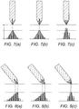
- Figures 7(a) to 7(c) are schematic illustrations of different stylus designs and their signal distributions in a vertical operation mode of the active stylus.
- Figures in the lower part of Figures 7(a) to 7(c) present tip signal distributions ('dress' shapes) for different stylus nib designs in the vertical operation mode of the active stylus in a direction parallel to the touch screen surface plane of the touch-sensitive display device, as received by a sensor matrix.
- Figure 7(a) shows the signal distribution for a conventional nib design comprising a tip electrode with long and narrow tip tail and without ring electrode.
- Figure 7(b) shows the signal distribution for a conventional nib design comprising a tip electrode with long and narrow tip tail and with a ring electrode surrounding the tip tail at about half of its total length.
- Figure 7(c) shows the signal distribution for the proposed single-unit (molded) nib portion with integrated tip and ring electrodes.
- the ability to control level, shape and/or size of the tip and ring electrodes in the proposed single-unit nib design enables to achieve narrower and more local tip signals for improved positioning of the active stylus in digitizer systems.
- Figure 9(a) shows an optical stack of an out-cell structure of the touch-sensitive display device, which includes a plurality of components configured to enable the reception of a touch input and the generation and presentation of a graphical output.
- a touch module is added onto a display module.
- the touch sensor may comprise a touch matrix of display electrodes that form capacitors whose capacitances may be evaluated in detecting touch input. More specifically, the electrodes may be formed in two separate layers: a receive electrode layer and a transmit electrode layer positioned below the receive electrode layer.
- receive and transmit electrode layers each may be formed on a respective dielectric substrate comprising materials including but not limited to glass, polyethylene terephthalate (PET), or cyclic olefin polymer (COP) film.
- PET polyethylene terephthalate
- COP cyclic olefin polymer
- the receive and transmit electrode layers may be bonded together by an optically-clear adhesive (not shown in Figure 9(a) ), which may be an acrylic pressure-sensitive adhesive film, for example.
- the touch sensor configuration may be integrally formed as a single layer with electrodes disposed on opposite surfaces of an integral layer. Further, the touch sensor may alternatively be configured such that the transmit electrode layer is provided above, and bonded, via the optically-clear adhesive, to receive an electrode layer positioned therebelow.
- the touch-sensitive display device may include a plurality of display electrodes whose capacitances may be evaluated in detecting a touch input, and these electrodes may be arranged or distributed in any suitable manner.
- the touch sensor may be bonded, e.g. at a bottom surface of the transmit electrode layer, to the lower display stack via a second optically-clear adhesive (OCA2) with a thickness of e.g. 150 ⁇ m.
- the lower display stack may comprise a polarization layer (Pol) with a thickness of e.g. 100 ⁇ m followed by a color filter (CF) glass layer with a thickness of e.g. 200 ⁇ m, a thin-film transistor (TFT) glass layer with a thickness of e.g. 200 ⁇ m and a final backlight unit (BLU) as a light source for the touch-sensitive display device.
- CF color filter
- TFT thin-film transistor
- on-cell and in-cell touch technologies are provided to overcome the drawbacks of traditional out-cell touch technology with additional weight and thickness of the touch display panel and reduced light penetration rate.
- Figure 9(c) shows an optical stack of an in-cell structure of the touch-sensitive display device, where the touch sensor (bold dashed line) is located between the color filter glass layer and the thin-film transistor glass layer.
- the in-cell technology is to dispose the sensor within the LCD cell structure to be integrated within the display unit, so that the display unit is provided with the ability of the touch panel. Therefore, the touch display panel does not need to be bonded with an additional touch panel and the assembly procedure can be simplified.
- the thickness of the first optically-clear adhesive (OCA1) is 100 ⁇ m here.
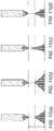
- Figures 10(a) to 10(c) are schematic cross-sectional views of respective stack designs of the different display touch module structures, where the on-cell and in-cell structures are without cover glass.
- the cover glass and the first optically-clear adhesive are removed in Figures 10(b) and 10(c) so that the distances of the on-cell and in-cell structures are reduced by 500 ⁇ m to 100 ⁇ m for the on-cell structure and 300 ⁇ m for the in-cell structure.
- the signal distribution is wider for the on-cell/in-cell display technology with cover glass and the signal level at the centre of the distribution is slightly lower, while the signal level at the centre of the distribution is much higher and the distribution is much narrower for the on-cell/in-cell display technology without cover glass (which is not good for stylus positioning).
- the distance between tip and ring electrodes and the antenna of the touch sensor can be adjusted individually based on the used display technology to provide better signal distribution and better accuracy.
- the nib portion may comprise respective connecting elements for electrically connecting the integrated tip and ring electrodes to signal processing circuits arranged in the housing.
- the nib portion may be releasably attachable to the housing.
- the signal processing circuits may comprise a controller adapted to determine an electrode configuration of the nib portion by measuring a predetermined parameter of the nib portion.
- the predetermined parameter may be selected from a capacitance between the tip and ring electrodes, a crosstalk between the tip and ring electrodes, and a resistance between the tip and ring electrodes.
- the controller may be adapted to transmit the nib identity to a touch-sensitive display device for which the stylus is used as input device.
- a nib portion with integrated tip and ring electrodes for use in a stylus of the above aspect and its embodiments.
- the nib portion may be made of a molded insulation material and the ring electrode may be printed on the molded insulation material.
- the tip and ring electrodes may be implemented as integrated parts of the nib portion, that are arranged deep inside the molded insulation material during the molding process or printed internally.
- a method comprising: determining an electrode configuration of a nib portion of a stylus by measuring a predetermined parameter of the nib portion; and calibrating the stylus by adapting stylus settings to the determined electrode configuration of the attached nib portion.
Landscapes
- Engineering & Computer Science (AREA)
- General Engineering & Computer Science (AREA)
- Theoretical Computer Science (AREA)
- Human Computer Interaction (AREA)
- Physics & Mathematics (AREA)
- General Physics & Mathematics (AREA)
- Position Input By Displaying (AREA)
Priority Applications (7)
| Application Number | Priority Date | Filing Date | Title |
|---|---|---|---|
| EP19195507.9A EP3789855A1 (de) | 2019-09-05 | 2019-09-05 | Taststiftspitzenentwurf und genauigkeitsverbesserung |
| PCT/US2020/049295 WO2021046281A1 (en) | 2019-09-05 | 2020-09-04 | Stylus nib design and accuracy improvement |
| EP20771959.2A EP4025985B1 (de) | 2019-09-05 | 2020-09-04 | Entwurf und genauigkeitsverbesserung einer spitze eines elektronischen stifts |
| CN202080062836.8A CN114341782B (zh) | 2019-09-05 | 2020-09-04 | 触控笔笔尖设计与精度改进 |
| US17/640,314 US11775086B2 (en) | 2019-09-05 | 2020-09-04 | Stylus nib design and accuracy improvement |
| CN202410374735.4A CN118170269A (zh) | 2019-09-05 | 2020-09-04 | 触控笔笔尖设计与精度改进 |
| US18/454,023 US20230393676A1 (en) | 2019-09-05 | 2023-08-22 | Stylus nib design and accuracy improvement |
Applications Claiming Priority (1)
| Application Number | Priority Date | Filing Date | Title |
|---|---|---|---|
| EP19195507.9A EP3789855A1 (de) | 2019-09-05 | 2019-09-05 | Taststiftspitzenentwurf und genauigkeitsverbesserung |
Publications (1)
| Publication Number | Publication Date |
|---|---|
| EP3789855A1 true EP3789855A1 (de) | 2021-03-10 |
Family
ID=67874276
Family Applications (2)
| Application Number | Title | Priority Date | Filing Date |
|---|---|---|---|
| EP19195507.9A Withdrawn EP3789855A1 (de) | 2019-09-05 | 2019-09-05 | Taststiftspitzenentwurf und genauigkeitsverbesserung |
| EP20771959.2A Active EP4025985B1 (de) | 2019-09-05 | 2020-09-04 | Entwurf und genauigkeitsverbesserung einer spitze eines elektronischen stifts |
Family Applications After (1)
| Application Number | Title | Priority Date | Filing Date |
|---|---|---|---|
| EP20771959.2A Active EP4025985B1 (de) | 2019-09-05 | 2020-09-04 | Entwurf und genauigkeitsverbesserung einer spitze eines elektronischen stifts |
Country Status (4)
| Country | Link |
|---|---|
| US (2) | US11775086B2 (de) |
| EP (2) | EP3789855A1 (de) |
| CN (2) | CN114341782B (de) |
| WO (1) | WO2021046281A1 (de) |
Cited By (1)
| Publication number | Priority date | Publication date | Assignee | Title |
|---|---|---|---|---|
| WO2022222662A1 (zh) * | 2021-04-23 | 2022-10-27 | Oppo广东移动通信有限公司 | 触控笔、触控笔系统及触控笔的控制方法 |
Families Citing this family (13)
| Publication number | Priority date | Publication date | Assignee | Title |
|---|---|---|---|---|
| WO2022044595A1 (ja) | 2020-08-25 | 2022-03-03 | 株式会社ワコム | ペンセンサ用カバーフィルム及びペンセンサ |
| US11656726B1 (en) * | 2022-02-09 | 2023-05-23 | Novatek Microelectronics Corp. | Control circuit, electronic device, and control method for stylus pen interacting with touch panel |
| US12299218B2 (en) | 2023-06-11 | 2025-05-13 | Remarkable As | Active pen-stylus precise eraser |
| CN118131923A (zh) * | 2022-12-02 | 2024-06-04 | Oppo广东移动通信有限公司 | 笔尖组件、电容笔以及电子设备组件 |
| CN115857712A (zh) * | 2022-12-16 | 2023-03-28 | 维沃移动通信有限公司 | 触控笔的笔尖类别检测方法、装置和触控笔 |
| CN116257145A (zh) * | 2023-03-28 | 2023-06-13 | 联想(北京)有限公司 | 一种笔尖组件、触控笔及制作笔尖组件的方法 |
| US20250099165A1 (en) * | 2023-09-26 | 2025-03-27 | Encision Inc. | Power estimation of distal end of electrosurgical instrument |
| USD1106208S1 (en) * | 2024-02-08 | 2025-12-16 | Remarkable As | Marker |
| USD1107023S1 (en) * | 2024-02-08 | 2025-12-23 | Remarkable As | Marker |
| USD1123935S1 (en) * | 2024-02-08 | 2026-04-28 | Remarkable As | Marker |
| CN121300641A (zh) | 2024-07-08 | 2026-01-09 | 瑞马科宝股份有限公司 | 标记笔保护系统 |
| CN121300642A (zh) * | 2024-07-08 | 2026-01-09 | 瑞马科宝股份有限公司 | 标记笔书写系统 |
| CN121300639A (zh) | 2024-07-08 | 2026-01-09 | 瑞马科宝股份有限公司 | 可更换导电标记笔尖端 |
Citations (3)
| Publication number | Priority date | Publication date | Assignee | Title |
|---|---|---|---|---|
| US20160091991A1 (en) * | 2014-09-30 | 2016-03-31 | Apple Inc. | Electronic Devices With Molded Insulator and Via Structures |
| US20180129310A1 (en) * | 2016-11-04 | 2018-05-10 | Microsoft Technology Licensing, Llc | Active Stylus |
| CN209311996U (zh) * | 2019-01-02 | 2019-08-27 | 陈梅珍 | 触控笔结构 |
Family Cites Families (33)
| Publication number | Priority date | Publication date | Assignee | Title |
|---|---|---|---|---|
| US8536471B2 (en) | 2008-08-25 | 2013-09-17 | N-Trig Ltd. | Pressure sensitive stylus for a digitizer |
| US8638320B2 (en) * | 2011-06-22 | 2014-01-28 | Apple Inc. | Stylus orientation detection |
| US8878823B1 (en) | 2011-07-27 | 2014-11-04 | Cypress Semiconductor Corporation | Dynamic shield electrode of a stylus |
| US9195351B1 (en) * | 2011-09-28 | 2015-11-24 | Amazon Technologies, Inc. | Capacitive stylus |
| US8878824B2 (en) | 2012-04-11 | 2014-11-04 | Blackberry Limited | Force-sensing stylus pointing device |
| US8913042B2 (en) | 2012-07-24 | 2014-12-16 | Blackberry Limited | Force sensing stylus |
| US9250721B2 (en) * | 2012-12-17 | 2016-02-02 | Disney Enterprises, Inc. | Wireless stylus device with interchangeable tips and eraser |
| WO2014127383A2 (en) | 2013-02-17 | 2014-08-21 | Zeliff Zachary Joseph | Stylus for capacitive touchscreen |
| TWI502459B (zh) * | 2013-07-08 | 2015-10-01 | Acer Inc | 電子裝置及其觸控操作方法 |
| US9513721B2 (en) | 2013-09-12 | 2016-12-06 | Microsoft Technology Licensing, Llc | Pressure sensitive stylus for a digitizer |
| US9983696B2 (en) | 2014-09-30 | 2018-05-29 | Apple Inc. | Force-sensing stylus for use with electronic devices |
| US20170300138A1 (en) * | 2014-10-03 | 2017-10-19 | Sharp Kabushiki Kaisha | Information input pen |
| US9612671B1 (en) | 2014-10-24 | 2017-04-04 | Amazon Technologies, Inc. | Stylus tip |
| JP6392449B2 (ja) * | 2015-04-08 | 2018-09-19 | シャープ株式会社 | 情報入力ペンおよび情報入力システム |
| CN112181175B (zh) * | 2015-04-20 | 2024-05-31 | 株式会社和冠 | 传感器控制器、主动式触控笔及使用了它们的方法 |
| US9874966B2 (en) * | 2015-04-28 | 2018-01-23 | Microsoft Technology Licensing, Llc | Electrostatic device having spaced electrodes |
| CN107787477A (zh) * | 2015-06-26 | 2018-03-09 | 三星电子株式会社 | 输入设备、用于接收来自输入设备的信号的电子设备及其控制方法 |
| US10168804B2 (en) | 2015-09-08 | 2019-01-01 | Apple Inc. | Stylus for electronic devices |
| US10025401B2 (en) | 2015-09-08 | 2018-07-17 | Apple Inc. | Active stylus ring electrode |
| US10198089B2 (en) | 2015-09-08 | 2019-02-05 | Apple Inc. | Active stylus precision tip |
| TW201730708A (zh) * | 2016-02-22 | 2017-09-01 | 翰碩電子股份有限公司 | 具有可置換導電筆芯之電容筆 |
| US9904379B2 (en) * | 2016-02-29 | 2018-02-27 | Apple Inc. | Disabling stylus to prevent worn tip performance degradation and screen damage |
| CN112416149B (zh) * | 2016-03-08 | 2024-08-20 | 禾瑞亚科技股份有限公司 | 侦测触控笔的倾斜角的触控控制装置与其控制方法 |
| US10048778B2 (en) | 2016-05-31 | 2018-08-14 | Microsoft Technology Licensing, Llc | Force sensor apparatus |
| US10296089B2 (en) | 2016-08-10 | 2019-05-21 | Microsoft Technology Licensing, Llc | Haptic stylus |
| KR20180050253A (ko) | 2016-09-29 | 2018-05-14 | 선전 구딕스 테크놀로지 컴퍼니, 리미티드 | 터치 스타일러스 펜 |
| TWI636383B (zh) | 2016-10-17 | 2018-09-21 | 禾瑞亞科技股份有限公司 | 觸控筆與其筆尖結構 |
| US10261604B2 (en) * | 2016-11-04 | 2019-04-16 | Microsoft Technology Licensing, Llc | Active stylus velocity correction |
| US10572063B2 (en) * | 2017-01-09 | 2020-02-25 | Microsoft Technology Licensing, Llc | Position, tilt, and twist detection for stylus |
| US10318022B2 (en) | 2017-01-30 | 2019-06-11 | Microsoft Technology Licensing, Llc | Pressure sensitive stylus |
| WO2020202352A1 (ja) * | 2019-03-29 | 2020-10-08 | 株式会社ワコム | ペン状態検出回路及びペン状態検出方法 |
| JP7346160B2 (ja) * | 2019-08-23 | 2023-09-19 | 株式会社ワコム | スタイラス及び集積回路 |
| US11175755B1 (en) * | 2020-06-08 | 2021-11-16 | Wacom Co., Ltd. | Input system and input method |
-
2019
- 2019-09-05 EP EP19195507.9A patent/EP3789855A1/de not_active Withdrawn
-
2020
- 2020-09-04 CN CN202080062836.8A patent/CN114341782B/zh active Active
- 2020-09-04 CN CN202410374735.4A patent/CN118170269A/zh active Pending
- 2020-09-04 US US17/640,314 patent/US11775086B2/en active Active
- 2020-09-04 EP EP20771959.2A patent/EP4025985B1/de active Active
- 2020-09-04 WO PCT/US2020/049295 patent/WO2021046281A1/en not_active Ceased
-
2023
- 2023-08-22 US US18/454,023 patent/US20230393676A1/en not_active Abandoned
Patent Citations (3)
| Publication number | Priority date | Publication date | Assignee | Title |
|---|---|---|---|---|
| US20160091991A1 (en) * | 2014-09-30 | 2016-03-31 | Apple Inc. | Electronic Devices With Molded Insulator and Via Structures |
| US20180129310A1 (en) * | 2016-11-04 | 2018-05-10 | Microsoft Technology Licensing, Llc | Active Stylus |
| CN209311996U (zh) * | 2019-01-02 | 2019-08-27 | 陈梅珍 | 触控笔结构 |
Cited By (1)
| Publication number | Priority date | Publication date | Assignee | Title |
|---|---|---|---|---|
| WO2022222662A1 (zh) * | 2021-04-23 | 2022-10-27 | Oppo广东移动通信有限公司 | 触控笔、触控笔系统及触控笔的控制方法 |
Also Published As
| Publication number | Publication date |
|---|---|
| CN114341782B (zh) | 2024-04-05 |
| CN114341782A (zh) | 2022-04-12 |
| WO2021046281A1 (en) | 2021-03-11 |
| US11775086B2 (en) | 2023-10-03 |
| EP4025985A1 (de) | 2022-07-13 |
| US20230393676A1 (en) | 2023-12-07 |
| CN118170269A (zh) | 2024-06-11 |
| EP4025985B1 (de) | 2025-12-03 |
| US20220334661A1 (en) | 2022-10-20 |
Similar Documents
| Publication | Publication Date | Title |
|---|---|---|
| EP4025985B1 (de) | Entwurf und genauigkeitsverbesserung einer spitze eines elektronischen stifts | |
| US11182036B2 (en) | Position, tilt, and twist detection for stylus | |
| US10452215B2 (en) | Mutual capacitive force sensor and touch display device with force sensing function and force sensing method thereof | |
| US20220147166A1 (en) | Sensor for detecting pen signal transmitted from pen | |
| EP2544081B1 (de) | Positionserkennungssensor, Positionserkennungsvorrichtung und Positionserkennungsverfahren | |
| KR102440965B1 (ko) | 스타일러스 펜, 스타일러스 펜으로부터 신호를 입력받는 전자 장치 및 이의 제어 방법 | |
| MX2011010298A (es) | Deteccion de tacto en una superficie curveada. | |
| CN109643176B (zh) | 触控笔、触摸感测系统、触摸感测控制器及触摸感测方法 | |
| US20170031509A1 (en) | Touch sensor | |
| US20210165510A1 (en) | Pen, Method for Detecting Pen, and Touch System | |
| US20140098030A1 (en) | Touch module | |
| KR20120004978A (ko) | 곡선형 표면 위의 터치 감지 방법 | |
| KR20150065656A (ko) | 사용자 입력의 유형들을 결정하는 시스템 및 방법 | |
| US20150177980A1 (en) | Touch sensor device and electronic device | |
| US20140247238A1 (en) | System and method for dual mode stylus detection | |
| US10261604B2 (en) | Active stylus velocity correction | |
| US10191601B2 (en) | Electronic device with touch control circuit powered by dedicated power source | |
| US20190087062A1 (en) | Force transfer element for edge force sensing | |
| US20170115753A1 (en) | Method for detecting orientation of stylus | |
| CN107346188A (zh) | 压力感应模组、终端、图像显示方法及装置 | |
| JP7025606B1 (ja) | ペンセンサ用カバーフィルム、ペンセンサ、及び電子機器 | |
| US20250123708A1 (en) | Sensor controller, electronic device, and control method of sensor controller | |
| CN109324700A (zh) | 可提供倾斜角与方位角侦测信号的电容笔 | |
| CN109857283A (zh) | 自参考电容性力传感器 | |
| JP6282223B2 (ja) | 入力機器 |
Legal Events
| Date | Code | Title | Description |
|---|---|---|---|
| PUAI | Public reference made under article 153(3) epc to a published international application that has entered the european phase |
Free format text: ORIGINAL CODE: 0009012 |
|
| STAA | Information on the status of an ep patent application or granted ep patent |
Free format text: STATUS: THE APPLICATION HAS BEEN PUBLISHED |
|
| AK | Designated contracting states |
Kind code of ref document: A1 Designated state(s): AL AT BE BG CH CY CZ DE DK EE ES FI FR GB GR HR HU IE IS IT LI LT LU LV MC MK MT NL NO PL PT RO RS SE SI SK SM TR |
|
| AX | Request for extension of the european patent |
Extension state: BA ME |
|
| RAP3 | Party data changed (applicant data changed or rights of an application transferred) |
Owner name: MICROSOFT TECHNOLOGY LICENSING, LLC |
|
| STAA | Information on the status of an ep patent application or granted ep patent |
Free format text: STATUS: THE APPLICATION IS DEEMED TO BE WITHDRAWN |
|
| 18D | Application deemed to be withdrawn |
Effective date: 20210911 |