EP3790113A1 - Dualbandantenne - Google Patents
Dualbandantenne Download PDFInfo
- Publication number
- EP3790113A1 EP3790113A1 EP20187178.7A EP20187178A EP3790113A1 EP 3790113 A1 EP3790113 A1 EP 3790113A1 EP 20187178 A EP20187178 A EP 20187178A EP 3790113 A1 EP3790113 A1 EP 3790113A1
- Authority
- EP
- European Patent Office
- Prior art keywords
- cwo
- value
- waveguide tube
- parameter
- electromagnetic wave
- Prior art date
- Legal status (The legal status is an assumption and is not a legal conclusion. Google has not performed a legal analysis and makes no representation as to the accuracy of the status listed.)
- Granted
Links
Images



Classifications
-
- H—ELECTRICITY
- H01—ELECTRIC ELEMENTS
- H01Q—ANTENNAS, i.e. RADIO AERIALS
- H01Q5/00—Arrangements for simultaneous operation of antennas on two or more different wavebands, e.g. dual-band or multi-band arrangements
- H01Q5/50—Feeding or matching arrangements for broad-band or multi-band operation
- H01Q5/55—Feeding or matching arrangements for broad-band or multi-band operation for horn or waveguide antennas
-
- H—ELECTRICITY
- H01—ELECTRIC ELEMENTS
- H01Q—ANTENNAS, i.e. RADIO AERIALS
- H01Q13/00—Waveguide horns or mouths; Slot antennas; Leaky-waveguide antennas; Equivalent structures causing radiation along the transmission path of a guided wave
- H01Q13/02—Waveguide horns
-
- H—ELECTRICITY
- H01—ELECTRIC ELEMENTS
- H01Q—ANTENNAS, i.e. RADIO AERIALS
- H01Q13/00—Waveguide horns or mouths; Slot antennas; Leaky-waveguide antennas; Equivalent structures causing radiation along the transmission path of a guided wave
- H01Q13/06—Waveguide mouths
-
- H—ELECTRICITY
- H01—ELECTRIC ELEMENTS
- H01Q—ANTENNAS, i.e. RADIO AERIALS
- H01Q19/00—Combinations of primary active antenna elements and units with secondary devices, e.g. with quasi-optical devices, for giving the antenna a desired directional characteristic
- H01Q19/10—Combinations of primary active antenna elements and units with secondary devices, e.g. with quasi-optical devices, for giving the antenna a desired directional characteristic using reflecting surfaces
-
- H—ELECTRICITY
- H01—ELECTRIC ELEMENTS
- H01Q—ANTENNAS, i.e. RADIO AERIALS
- H01Q19/00—Combinations of primary active antenna elements and units with secondary devices, e.g. with quasi-optical devices, for giving the antenna a desired directional characteristic
- H01Q19/10—Combinations of primary active antenna elements and units with secondary devices, e.g. with quasi-optical devices, for giving the antenna a desired directional characteristic using reflecting surfaces
- H01Q19/18—Combinations of primary active antenna elements and units with secondary devices, e.g. with quasi-optical devices, for giving the antenna a desired directional characteristic using reflecting surfaces having two or more spaced reflecting surfaces
- H01Q19/19—Combinations of primary active antenna elements and units with secondary devices, e.g. with quasi-optical devices, for giving the antenna a desired directional characteristic using reflecting surfaces having two or more spaced reflecting surfaces comprising one main concave reflecting surface associated with an auxiliary reflecting surface
-
- H—ELECTRICITY
- H01—ELECTRIC ELEMENTS
- H01Q—ANTENNAS, i.e. RADIO AERIALS
- H01Q5/00—Arrangements for simultaneous operation of antennas on two or more different wavebands, e.g. dual-band or multi-band arrangements
- H01Q5/40—Imbricated or interleaved structures; Combined or electromagnetically coupled arrangements, e.g. comprising two or more non-connected fed radiating elements
- H01Q5/45—Imbricated or interleaved structures; Combined or electromagnetically coupled arrangements, e.g. comprising two or more non-connected fed radiating elements using two or more feeds in association with a common reflecting, diffracting or refracting device
- H01Q5/47—Imbricated or interleaved structures; Combined or electromagnetically coupled arrangements, e.g. comprising two or more non-connected fed radiating elements using two or more feeds in association with a common reflecting, diffracting or refracting device with a coaxial arrangement of the feeds
Definitions
- the present application relates to the field of wireless communications, and in particular, to a coaxial dual-band antenna that can be used in a dual-band parabolic antenna.
- an E-band (71 to 76 GHz, 81 to 86 GHz) frequency band microwave device plays an increasingly important role in a base station backhaul network.
- an E-band microwave single-hop distance is usually less than 3 kilometers.
- the E-band frequency band microwave device and another low frequency microwave device are cooperatively used. When there is relatively heavy rain, even if the E-band microwave device cannot normally work, the low frequency microwave device can still normally work.
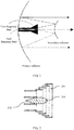
- a dual-band parabolic antenna is used in this solution, and a structure of the dual-band parabolic antenna is shown in FIG. 1 .
- the dual-band parabolic antenna includes a primary reflector, a secondary reflector, a low frequency feed, and a high frequency feed.
- the high frequency feed is inserted into the low frequency feed, and the two feeds use a same axis, and form a coaxial dual-band antenna.
- the two feeds of the coaxial dual-band antenna share the primary reflector and the secondary reflector, and phase centers of the two feeds are overlapped at a focus of the secondary reflector, so as to implement a dual-band multiplexing function.
- a low frequency feed of a coaxial dual-band antenna is usually in a shape of a large-mouth horn, and a dielectric pin needs to be inserted into a high frequency feed.
- Both the high frequency feed and the low frequency feed have problems that radiation efficiency is relatively low, and a gain cannot reach a gain level of a single-band antenna.
- Embodiments of the present application provide a coaxial dual-band antenna.
- a circular waveguide with an unchanged diameter or a circular waveguide with a small flare angle is used to replace a large-mouth horn-shaped waveguide and serves as a low frequency feed, so as to resolve problems that radiation efficiency of a high frequency feed and a low frequency feed in an existing coaxial dual-band antenna is relatively low, and a gain cannot reach a gain level of a single-band antenna.
- a coaxial dual-band antenna includes a waveguide tube, a ring groove, a high frequency feed, and a dielectric ring, where the waveguide tube has a tubular structure, and is configured to transmit a first electromagnetic wave, the ring groove whose opening direction is the same as an output direction of the first electromagnetic wave is on a wall of the waveguide tube, and a frequency of the first electromagnetic wave is lower than a frequency of an electromagnetic wave transmitted by the high frequency feed; the high frequency feed is located in the waveguide tube, and has a same axis with the waveguide tube, and the first electromagnetic wave excites a transverse electric mode TE 11 in the waveguide tube; and; and the dielectric ring is filled between the waveguide tube and the high frequency feed, the dielectric ring has a multi-layer structure, and has a same axis with the waveguide tube, area sizes of planes that are at layers of the dielectric ring and that are perpendicular to the axis alternately change, and a
- the coaxial dual-band antenna excites the TE 11 mode of the first electromagnetic wave at a low frequency, and no high order mode is generated inside the waveguide tube. This avoids a transmission loss of a high order mode in the waveguide, and improves low frequency radiation efficiency of the dual-band antenna. In addition, because no high order mode is generated inside the waveguide tube, there is no need to worry about that the high frequency feed located in the waveguide tube affects electromagnetic field distribution of the high order mode. Therefore, a dielectric pin can be omitted, and high frequency radiation efficiency of the dual-band antenna can be improved.
- a height of the high frequency feed is the same as the height of the waveguide tube.
- a sum of a radius of an inner wall of the waveguide tube and a radius of an outer wall of the high frequency feed is greater than 1/ ⁇ of a wavelength of the first electromagnetic wave, and a difference between the two radiuses is less than 1/2 of the wavelength of the first electromagnetic wave.
- a difference between a radius of the ring groove and the radius of the inner wall of the waveguide tube is 1/8 of the wavelength of the first electromagnetic wave.
- a depth of the ring groove is between 1/5 and 1/4 of the wavelength of the first electromagnetic wave, and a width of the ring groove is 1/8 of the wavelength of the first electromagnetic wave.
- Size requirements of the ring groove are provided in the foregoing two embodiments.
- a high order mode excited by a ring groove meeting the size requirements may be overlaid with the TE 11 mode, so that a beam width of the first electromagnetic wave on an E plane is consistent with that on an H plane, and radiation efficiency of the first electromagnetic wave is maximized.
- an outer wall at only one of two adjacent layers of the dielectric ring is connected to the inner wall of the waveguide tube, and an inner wall at the layer of the dielectric ring is connected to the outer wall of the high frequency feed. This can implement sealing and waterproof functions, and can fasten the high frequency feed.
- a layer that is of the dielectric ring and that is farthest from an output plane of the waveguide tube is not connected to the waveguide tube and the high frequency feed at a same time. This can reduce reflection of the first electromagnetic wave on the dielectric ring, and improve radiation efficiency.
- a height of each layer of the dielectric ring is 1/4 of the wavelength of the first electromagnetic wave.
- a relative dielectric constant of the dielectric ring is between 2 and 4.
- each layer of the dielectric ring and the relative dielectric constant are described in the foregoing two embodiments.
- the height of each layer of the dielectric ring and the relative dielectric constant enable characteristic impedance of the coaxial dual-band antenna and wave impedance of free space to match each other, and improve the radiation efficiency.
- the coaxial dual-band antenna provided in the present application excites a TE 11 mode of a first electromagnetic wave at a low frequency, and no high order mode is generated inside a waveguide tube. This avoids a transmission loss of a high order mode in the waveguide, and improves low frequency radiation efficiency of the dual-band antenna. In addition, because no high order mode is generated inside the waveguide tube, there is no need to worry about that a high frequency feed located in the waveguide tube affects electromagnetic field distribution of the high order mode. Therefore, a dielectric pin can be omitted, and high frequency radiation efficiency of the dual-band antenna can be improved.
- a structure of an existing coaxial dual-band antenna is shown in FIG. 2 .
- a low frequency feed 201 of the coaxial dual-band antenna is a large-mouth horn-shaped waveguide, a high frequency feed 202 is included in the waveguide, and a dielectric pin 203 is inserted into the high frequency feed 202.
- the horn-shaped waveguide is used to facilitate matching between characteristic impedance of the waveguide and wave impedance of free space, so as to reduce reflection.
- a radius of the waveguide increases, a high order mode is excited, and the high order mode and a transverse electric mode TE 11 take effect, so that a beam width of an output electromagnetic wave on an E plane is consistent with that on an H plane, and a best gain effect is achieved.
- the E plane is a plane including a direction in which an electric field is located and a direction with highest radiation intensity
- the H plane is a plane including a direction in which a magnetic field is located and the direction with the highest radiation intensity.
- the high order mode is generated inside the large-mouth horn-shaped waveguide, and a transmission loss in the waveguide is relatively large. Therefore, low frequency radiation efficiency of the dual-band antenna is relatively low.
- the high frequency feed is metallic, and affects electromagnetic field distribution of the high order mode. Therefore, the high frequency feed cannot directly extend to an aperture of the large-mouth horn-shaped waveguide, and a dielectric pin needs to guide a phase center of the high frequency feed to the aperture of the large-mouth horn-shaped waveguide.
- processing of the dielectric pin is uneasy, and a loss of the dielectric pin is relatively large. Therefore, a high frequency gain of the dual-band antenna cannot reach a level of a single-band antenna, either.
- the antenna includes a waveguide tube 301, a ring groove 302, a high frequency feed 303, and a dielectric ring 304.
- the waveguide tube 301 has a tubular structure, and is configured to transmit a first electromagnetic wave, the ring groove 302 whose opening direction is the same as an output direction of the first electromagnetic wave is on a wall of the waveguide tube 301, and a frequency of the first electromagnetic wave is lower than a frequency of an electromagnetic wave transmitted by the high frequency feed 303.
- the high frequency feed 303 is located in the waveguide tube 301, and has a same axis with the waveguide tube 301, and the first electromagnetic wave excites a transverse electric mode TE 11 in the waveguide tube 301.
- the dielectric ring 304 is filled between the waveguide tube 301 and the high frequency feed 303.
- the dielectric ring 304 has a multi-layer structure, and has a same axis with the waveguide tube 301. Area sizes of planes that are at layers of the dielectric ring 304 and that are perpendicular to the axis alternately change. A height of the dielectric ring 304 is less than a height of the waveguide tube 301.
- a height of the high frequency feed 303 is the same as the height of the waveguide tube 301. It should be understood that, it is also feasible if the height of the high frequency feed is slightly less than the height of the waveguide tube.
- a waveguide tube excites a TE 11 mode of a first electromagnetic wave at a low frequency, and no high order mode is generated inside the waveguide tube.
- no high order mode is generated inside the waveguide tube, there is no need to worry about that a high frequency feed located in the waveguide tube affects electromagnetic field distribution of the high order mode. Therefore, a dielectric pin can be omitted, and high frequency radiation efficiency of the dual-band antenna can be improved.
- an inner wall of the dielectric ring 304 is connected to an outer wall of the high frequency feed 303.
- an outer wall of the dielectric ring 304 may be connected to an inner wall of the waveguide tube 301; or, as shown in FIG.
- an inner wall at one or more layers of the dielectric ring 304 may be connected to an outer wall of the high frequency feed 303, and an outer wall at a remaining layer of the dielectric ring is connected to an inner wall of the waveguide tube 301.
- electromagnetic field distribution on a cross section of a waveguide is referred to as a propagation mode of the waveguide.
- Different propagation modes have different cut-off wavelengths, a mode without a cut-off wavelength or with a longest cut-off wavelength is referred to as a dominant mode or a base mode, and another mode with a shorter cut-off wavelength is referred to as a high order mode.
- a higher order of a propagation mode indicates a shorter cut-off wavelength.
- the TE 11 mode is used as the base mode, and another mode with a cut-off wavelength shorter than that of the TE 11 mode is referred to as a high order mode.
- the waveguide tube provided in this embodiment of the present application may be in a shape of a cylinder, a rectangular tube, or the like.
- a mouth for outputting the first electromagnetic wave may be slightly expanded, provided that only the base mode of the first electromagnetic wave is excited in the coaxial dual-band antenna including the waveguide tube, the high frequency feed, the ring groove, and the dielectric ring.
- a wall of the waveguide tube is usually metallic.
- a sum of a radius of the inner wall of the waveguide tube 301 and a radius of the outer wall of the high frequency feed 303 is greater than 1/ ⁇ of a wavelength of the first electromagnetic wave, a difference between the two radiuses is less than 1/2 of the wavelength of the first electromagnetic wave, and a frequency of the first electromagnetic wave is lower than a frequency of an electromagnetic wave transmitted by the high frequency feed 303.
- the coaxial waveguide including the high frequency feed 303 and the waveguide tube 301 in the present application is used as an example.
- Cut-off wavelengths of the first electromagnetic wave in different modes are related to an outer radius a of an inner waveguide (the radius of the outer wall of the high frequency feed 303) and an inner radius b of an outer waveguide (the radius of the inner wall of the waveguide tube 301) in the coaxial waveguide.
- a correspondence is listed in Table 1.
- the first electromagnetic wave may excite the TE 11 mode if the coaxial waveguide meets a condition in which (b + a) > ⁇ / ⁇ and (b - a) ⁇ ⁇ /2. If b in the coaxial waveguide becomes larger, and consequently (b - a) > ⁇ /2 and (b + a) ⁇ 2 ⁇ / ⁇ , the first electromagnetic wave may excite modes such as TE 11 , TM m1 , and TE 01 in theory.
- modes such as TE 11 , TM m1 , and TE 01 in theory.
- a continuous tangential component needs to be ensured when an electromagnetic field mode changes, that is, m needs to be consistent. Therefore, only two modes actually exist: TE 11 and TM 11 . As the inner radius b of the outer waveguide in the coaxial waveguide increases, more modes exist gradually.
- a transverse electromagnetic mode TEM may also exist in the coaxial waveguide, and no cut-off wavelength exists in this mode or a cut-off wavelength in this mode is infinitely long.
- the TEM mode is suppressed in a symmetrical feeding manner. Therefore, this mode is not considered in this embodiment of the present application.
- the ring groove 302 whose opening direction is the same as the output direction of the first electromagnetic wave is excavated on the wall of the waveguide tube 301, a high order mode is excited by using discontinuity of the wall of the waveguide tube 301, and the high order mode is used to make the electric field distribution of the TE 11 mode become uniform.
- a depth and a width of the ring groove 302 and a distance from the ring groove 302 to the inner wall of the waveguide tube 301 all affect an order and amplitude of the high order mode.
- a difference between a radius of the ring groove 302 and the radius of the inner wall of the waveguide tube 301 is 1/8 of the wavelength of the first electromagnetic wave.
- the depth of the ring groove 302 is between 1/5 and 1/4 of the wavelength of the first electromagnetic wave, and the width of the ring groove 302 is 1/8 of the wavelength of the first electromagnetic wave.
- the ring groove 302 causes discontinuity on a surface of the wall, so that the high order mode is excited.
- the location, the width, and the depth of the ring groove 302 meet the foregoing requirements, so that the high order mode TM 11 with an appropriate amplitude can be generated.
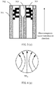
- Electric field distribution of the TM 11 mode is shown in FIG. 4 (b) .
- FIG. 4 (c) the TE 11 mode and the TM 11 mode are overlaid, so that the electric field distribution of the first electromagnetic wave becomes uniform. Consequently, the beam width of the first electromagnetic wave on the E plane is consistent with that on the H plane, and a gain effect is maximized.
- impedance matching may be implemented in the following two manners.
- the dielectric ring 304 filled between the waveguide tube 301 and the high frequency feed 303 is used to implement impedance matching.
- the dielectric ring 304 has the multi-layer structure, and has the same axis with the waveguide tube 301.
- the area sizes of the planes that are at the layers of the dielectric ring 304 and that are perpendicular to the axis alternately change.
- the height of the dielectric ring 304 is less than the height of the waveguide tube 301.
- the structure of the dielectric ring 304 may be any structure shown in FIG. 3 (a), FIG. 3 (b) , and FIG. 3 (c) .
- R 0 is the characteristic impedance of the waveguide
- R L is the load impedance
- the load impedance is the wave impedance of the free space
- the characteristic impedance of the waveguide is the characteristic impedance of the coaxial dual-band antenna.
- the characteristic impedance of the waveguide tube can be changed by filling a dielectric in the waveguide tube. That is, the filled dielectric ring forms the matching section.
- the waveguide tube is fully filled with the dielectric, in the waveguide tube, a sudden change of the characteristic impedance occurs on a contact surface between the dielectric and the air, and there is strong reflection.
- the dielectric ring 304 used in the present application does not fully fill a gap between the waveguide tube 301 and the high frequency feed 303, but uses the multi-layer structure having the same axis with the waveguide tube 301.
- the area sizes of the planes that are at the layers of the dielectric ring 304 and that are perpendicular to the axis alternately change, to form a mixture of the dielectric and the air. Therefore, an equivalent relative dielectric constant is no longer equal to a relative dielectric constant of a material, and can be controlled and changed.
- a purpose of such control and change is to enable the characteristic impedance of the matching section to reach a value obtained by means of calculation by using the foregoing formula.
- a height of each layer of the dielectric ring 304 is 1/4 of the wavelength of the first electromagnetic wave, and the first electromagnetic wave is a low frequency electromagnetic wave transmitted by the coaxial dual-band antenna.
- an outer wall at only one of two adjacent layers of the dielectric ring 304 is connected to the inner wall of the waveguide tube 301, and an inner wall at the layer of the dielectric ring 304 is connected to the outer wall of the high frequency feed 303.
- inner walls at multiple layers of the dielectric ring 304 are connected to the outer wall of the high frequency feed 303, and outer walls at the multiple layers of the dielectric ring 304 are connected to the inner wall of the waveguide tube 301.
- This can implement air sealing and waterproof functions, and can fasten the high frequency feed 303 in between.
- the coaxial dual-band antenna not only can be applied to satellite communication, but also is applicable to the ground.
- spacing between an inner wall and an outer wall at another layer of the dielectric ring 304 needs to be designed and optimized according to the foregoing equivalent dielectric constant principle.
- a layer that is of the dielectric ring 304 and that is farthest from an output plane of the waveguide tube 301 is not connected to the waveguide tube 301 and the high frequency feed 303 at a same time, so as to reduce reflection of the first electromagnetic wave.
- the layer that is of the dielectric ring and that is farthest from the output plane is a bottom layer of the dielectric ring shown in FIG. 5 (a) and FIG. 5 (b) .
- a dielectric material whose relative dielectric constant is between 2 and 4 may be used for the dielectric ring in this embodiment of the present application, for example, polycarbonate, polystyrene, and polytetrafluorethylene.
- a specific material is not limited in this embodiment of the present application.
- spacing between an inner wall and an outer wall at each layer of the dielectric ring 304 is further related to the wavelength of the first electromagnetic wave.
- the following provides a specific embodiment in which the frequency of the first electromagnetic wave is 18 GHz. It is assumed that polycarbonate whose relative dielectric constant is 2.8 is used to prepare the dielectric ring, the radius of the inner wall of the waveguide tube is R, and the dielectric ring has six layers. As shown in FIG.
- radius lengths of layers of the dielectric ring alternately change from top to bottom, radiuses of outer walls at the first layer, the third layer, and the fifth layer of the dielectric ring are R, a radius of an outer wall at the second layer of the dielectric ring is 0.78R, a radius of an outer wall at the fourth layer of the dielectric ring is 0.7R, and a radius of an outer wall at the sixth layer of the dielectric ring is 0.7R.
- the characteristic impedance of the matching section can meet formula (1) by using the dielectric ring with the foregoing sizes, so that the characteristic impedance of the coaxial dual-band antenna and the wave impedance of the free space match each other, electromagnetic wave reflection is reduced, and radiation efficiency is improved.
- each metal ring 601 is disposed in the waveguide tube to implement impedance matching.
- the metal rings form a matching section.
- a possible structure is shown in FIG. 6 (a) , and an inner wall of each metal ring 601 is connected to the outer wall of the high frequency feed 303.
- Equivalent inductance and equivalent capacitance of each metal ring 601 may be changed by changing a radius of each metal ring 601 and spacing between the metal rings 601, so that characteristic impedance of the matching section reaches a value obtained by means of calculation by using formula (1).
- a dielectric layer 602 may further be filled at a location that is inside the waveguide tube 301 and that is close to the output plane. As shown in FIG. 6 (b) , an inner wall of the dielectric layer 602 is connected to the outer wall of the high frequency feed 303, and an outer wall of the dielectric layer 602 is connected to the inner wall of the waveguide tube 301. This can implement air sealing and waterproof functions, and can fasten the high frequency feed.
- a hard material may be used for the dielectric layer 602, and a specific material is not limited in the present application.
- FIG. 6 (a) and FIG. 6 (b) show only possible structures in this embodiment of the present application.
- outer walls of the metal rings 601 may be connected to the inner wall of the waveguide tube 301, to form a matching section.
- outer walls of some metal rings 601 are connected to the inner wall of the waveguide tube 301, and inner walls of the other part of metal rings 601 are connected to the outer wall of the high frequency feed 303, to form a matching section.
- a specific implementation is not limited in this embodiment of the present application.
- the coaxial dual-band antenna provided in the present application has the following advantages: A waveguide tube 301 excites a TE 11 mode of a first electromagnetic wave at a low frequency, and no high order mode is generated inside the waveguide tube 301. This avoids a transmission loss of a high order mode in the waveguide tube 301, and improves low frequency radiation efficiency of the dual-band antenna. In addition, because no high order mode is generated inside the waveguide tube 301, there is no need to worry about that a high frequency feed 303 located in the waveguide tube 301 affects electromagnetic field distribution of the high order mode. Therefore, a dielectric pin can be omitted, and high frequency radiation efficiency of the dual-band antenna can be improved.
- a beam width of the first electromagnetic wave on an E plane can be consistent with that on an H plane, and characteristic impedance of the coaxial dual-band antenna and wave impedance of free space can match each other.
- Embodiment 1 A coaxial dual-band antenna, comprising: a waveguide tube, a ring groove, a high frequency feed, and a dielectric ring, wherein the waveguide tube has a tubular structure, and is configured to transmit a first electromagnetic wave, the ring groove whose opening direction is the same as an output direction of the first electromagnetic wave is on a wall of the waveguide tube, and a frequency of the first electromagnetic wave is lower than a frequency of an electromagnetic wave transmitted by the high frequency feed; the high frequency feed is located in the waveguide tube, and has a same axis with the waveguide tube, and the first electromagnetic wave excites a transverse electric mode TE 11 in the waveguide tube; and the dielectric ring is filled between the waveguide tube and the high frequency feed, the dielectric ring has a multi-layer structure, and has a same axis with the waveguide tube, area sizes of planes that are at layers of the dielectric ring and that are perpendicular to the axis alternately change, and a height of the
- Embodiment 2 The antenna according to embodiment 1, wherein a height of the high frequency feed is the same as the height of the waveguide tube.
- Embodiment 3 The antenna according to embodiment 1, wherein a sum of a radius of an inner wall of the waveguide tube and a radius of an outer wall of the high frequency feed is greater than 1/ ⁇ of a wavelength of the first electromagnetic wave, and a difference between the two radiuses is less than 1/2 of the wavelength of the first electromagnetic wave.
- Embodiment 4 The antenna according to any one of embodiments 1 to 3, wherein a difference between a radius of the ring groove and the radius of the inner wall of the waveguide tube is 1/8 of the wavelength of the first electromagnetic wave.
- Embodiment 5 The antenna according to embodiment 4, wherein a depth of the ring groove is between 1/5 and 1/4 of the wavelength of the first electromagnetic wave, and a width of the ring groove is 1/8 of the wavelength of the first electromagnetic wave.
- Embodiment 6 The antenna according to any one of embodiments 1 to 3, wherein an outer wall at only one of two adjacent layers of the dielectric ring is connected to the inner wall of the waveguide tube, and an inner wall at the layer of the dielectric ring is connected to the outer wall of the high frequency feed.
- Embodiment 7 The antenna according to embodiment 6, wherein a layer that is of the dielectric ring and that is farthest from an output plane of the waveguide tube is not connected to the waveguide tube and the high frequency feed at a same time.
- Embodiment 8 The antenna according to embodiment 6, wherein a height of each layer of the dielectric ring is 1/4 of the wavelength of the first electromagnetic wave.
- Embodiment 9 The antenna according to embodiment 6, wherein a relative dielectric constant of the dielectric ring is between 2 and 4.
Landscapes
- Physics & Mathematics (AREA)
- Electromagnetism (AREA)
- Waveguide Aerials (AREA)
Priority Applications (1)
| Application Number | Priority Date | Filing Date | Title |
|---|---|---|---|
| EP20187178.7A EP3790113B1 (de) | 2017-01-22 | 2017-01-22 | Dualbandantenne |
Applications Claiming Priority (3)
| Application Number | Priority Date | Filing Date | Title |
|---|---|---|---|
| EP20187178.7A EP3790113B1 (de) | 2017-01-22 | 2017-01-22 | Dualbandantenne |
| EP17893209.1A EP3419113B1 (de) | 2017-01-22 | 2017-01-22 | Doppelfrequenzantenne |
| PCT/CN2017/072085 WO2018133071A1 (zh) | 2017-01-22 | 2017-01-22 | 一种双频天线 |
Related Parent Applications (2)
| Application Number | Title | Priority Date | Filing Date |
|---|---|---|---|
| EP17893209.1A Division-Into EP3419113B1 (de) | 2017-01-22 | 2017-01-22 | Doppelfrequenzantenne |
| EP17893209.1A Division EP3419113B1 (de) | 2017-01-22 | 2017-01-22 | Doppelfrequenzantenne |
Publications (2)
| Publication Number | Publication Date |
|---|---|
| EP3790113A1 true EP3790113A1 (de) | 2021-03-10 |
| EP3790113B1 EP3790113B1 (de) | 2023-03-08 |
Family
ID=62907562
Family Applications (2)
| Application Number | Title | Priority Date | Filing Date |
|---|---|---|---|
| EP20187178.7A Active EP3790113B1 (de) | 2017-01-22 | 2017-01-22 | Dualbandantenne |
| EP17893209.1A Active EP3419113B1 (de) | 2017-01-22 | 2017-01-22 | Doppelfrequenzantenne |
Family Applications After (1)
| Application Number | Title | Priority Date | Filing Date |
|---|---|---|---|
| EP17893209.1A Active EP3419113B1 (de) | 2017-01-22 | 2017-01-22 | Doppelfrequenzantenne |
Country Status (6)
| Country | Link |
|---|---|
| US (2) | US10916849B2 (de) |
| EP (2) | EP3790113B1 (de) |
| JP (1) | JP6707269B2 (de) |
| CN (2) | CN112821076A (de) |
| PL (1) | PL3419113T3 (de) |
| WO (1) | WO2018133071A1 (de) |
Cited By (1)
| Publication number | Priority date | Publication date | Assignee | Title |
|---|---|---|---|---|
| US12555907B1 (en) | 2023-10-04 | 2026-02-17 | Bae Systems Information And Electronic Systems Integration Inc. | Integrated dual frequency band antenna assembly |
Families Citing this family (12)
| Publication number | Priority date | Publication date | Assignee | Title |
|---|---|---|---|---|
| CN109478725B (zh) * | 2016-09-23 | 2021-06-29 | 康普技术有限责任公司 | 双频带抛物面反射器微波天线系统 |
| US11367964B2 (en) * | 2018-01-02 | 2022-06-21 | Optisys, LLC | Dual-band integrated printed antenna feed |
| WO2020019264A1 (zh) * | 2018-07-26 | 2020-01-30 | 华为技术有限公司 | 一种馈源装置、双频微波天线及双频天线设备 |
| US11424538B2 (en) | 2018-10-11 | 2022-08-23 | Commscope Technologies Llc | Feed systems for multi-band parabolic reflector microwave antenna systems |
| GB2585102B (en) * | 2019-10-09 | 2021-06-30 | Audio Inventions Ltd | System for identification of a note played by a musical instrument |
| CN111129730B (zh) * | 2019-12-20 | 2024-04-26 | 京信通信技术(广州)有限公司 | 天线及其双频辐射结构 |
| US20240030617A1 (en) * | 2020-09-25 | 2024-01-25 | Telefonaktiebolaget Lm Ericsson (Publ) | Antenna and method |
| CN118160157A (zh) * | 2021-11-19 | 2024-06-07 | 华为技术有限公司 | 一种双频馈源、天线设备和无线通信设备 |
| CN114361767B (zh) * | 2021-12-24 | 2024-02-20 | 广东盛路通信科技股份有限公司 | 一种宽频带天线馈源及微波天线 |
| CN114628891B (zh) * | 2022-02-28 | 2023-12-08 | 南京邮电大学 | 内嵌馈电线极化平面多层异质介质集成天线 |
| KR102711577B1 (ko) * | 2022-10-21 | 2024-10-02 | (주)인텔리안테크놀로지스 | 피드혼 |
| CN118299802B (zh) * | 2024-03-28 | 2025-11-14 | 电子科技大学 | 应用于毫米波探测的Ka/V波段双频锥状波束天线 |
Citations (3)
| Publication number | Priority date | Publication date | Assignee | Title |
|---|---|---|---|---|
| US5793334A (en) * | 1996-08-14 | 1998-08-11 | L-3 Communications Corporation | Shrouded horn feed assembly |
| US20080297428A1 (en) * | 2006-02-24 | 2008-12-04 | Northrop Grumman Corporation | High-power dual-frequency coaxial feedhorn antenna |
| US20110291903A1 (en) * | 2010-05-27 | 2011-12-01 | Orbit Communication System Ltd. | Multi band telemetry antenna feed |
Family Cites Families (22)
| Publication number | Priority date | Publication date | Assignee | Title |
|---|---|---|---|---|
| JPS6095710A (ja) | 1983-10-29 | 1985-05-29 | Alps Electric Co Ltd | 補助磁極励磁型垂直磁気記録用磁気ヘツド |
| JPS6095710U (ja) * | 1983-12-06 | 1985-06-29 | 三菱電機株式会社 | ホ−ンアンテナ |
| US4740795A (en) * | 1986-05-28 | 1988-04-26 | Seavey Engineering Associates, Inc. | Dual frequency antenna feeding with coincident phase centers |
| US5041840A (en) * | 1987-04-13 | 1991-08-20 | Frank Cipolla | Multiple frequency antenna feed |
| JP2825261B2 (ja) * | 1989-04-03 | 1998-11-18 | 株式会社東芝 | 同軸ホーンアンテナ |
| US4998113A (en) * | 1989-06-23 | 1991-03-05 | Hughes Aircraft Company | Nested horn radiator assembly |
| US5907309A (en) * | 1996-08-14 | 1999-05-25 | L3 Communications Corporation | Dielectrically loaded wide band feed |
| US6577283B2 (en) * | 2001-04-16 | 2003-06-10 | Northrop Grumman Corporation | Dual frequency coaxial feed with suppressed sidelobes and equal beamwidths |
| US6677911B2 (en) * | 2002-01-30 | 2004-01-13 | Prodelin Corporation | Antenna feed assembly capable of configuring communication ports of an antenna at selected polarizations |
| US6700549B2 (en) * | 2002-03-13 | 2004-03-02 | Ydi Wireless, Inc. | Dielectric-filled antenna feed |
| US7079079B2 (en) * | 2004-06-30 | 2006-07-18 | Skycross, Inc. | Low profile compact multi-band meanderline loaded antenna |
| US7379030B1 (en) * | 2004-11-12 | 2008-05-27 | Lockheed Martin Corporation | Artificial dielectric antenna elements |
| CN102394374B (zh) * | 2011-06-29 | 2013-08-28 | 西安空间无线电技术研究所 | 一种双频馈源 |
| US9520637B2 (en) * | 2012-08-27 | 2016-12-13 | Kvh Industries, Inc. | Agile diverse polarization multi-frequency band antenna feed with rotatable integrated distributed transceivers |
| DE102013011651A1 (de) * | 2013-07-11 | 2015-01-15 | ESA-microwave service GmbH | Antennen-Speisesystem im Mikrowellenbereich für Reflektorantennen |
| CN103490167A (zh) * | 2013-08-14 | 2014-01-01 | 京信通信技术(广州)有限公司 | 高增益滤波天线 |
| US9300042B2 (en) * | 2014-01-24 | 2016-03-29 | Honeywell International Inc. | Matching and pattern control for dual band concentric antenna feed |
| CN104600435A (zh) * | 2014-12-27 | 2015-05-06 | 广东盛路通信科技股份有限公司 | 一种用作抛物面馈源的分形介质谐振天线 |
| US10193234B2 (en) * | 2015-01-29 | 2019-01-29 | Speedcast International Limited | Method for upgrading a satellite antenna assembly and an associated upgradable satellite antenna assembly |
| CN104901020B (zh) * | 2015-05-08 | 2018-03-23 | 中国电子科技集团公司第五十四研究所 | 一种多频段反射面天线 |
| CN105428815B (zh) * | 2015-12-29 | 2018-11-06 | 南京逸然电子科技有限公司 | 一种全金属宽频带的高增益低剖面谐振天线 |
| CN205723956U (zh) * | 2016-06-20 | 2016-11-23 | 中国电子科技集团公司第三十八研究所 | 一种多频段双极化大功率馈源 |
-
2017
- 2017-01-22 CN CN202110008312.7A patent/CN112821076A/zh active Pending
- 2017-01-22 PL PL17893209T patent/PL3419113T3/pl unknown
- 2017-01-22 EP EP20187178.7A patent/EP3790113B1/de active Active
- 2017-01-22 JP JP2019506088A patent/JP6707269B2/ja active Active
- 2017-01-22 WO PCT/CN2017/072085 patent/WO2018133071A1/zh not_active Ceased
- 2017-01-22 EP EP17893209.1A patent/EP3419113B1/de active Active
- 2017-01-22 CN CN201780014019.3A patent/CN108701900B/zh active Active
-
2018
- 2018-09-18 US US16/134,519 patent/US10916849B2/en active Active
-
2020
- 2020-11-23 US US17/101,826 patent/US11652294B2/en active Active
Patent Citations (3)
| Publication number | Priority date | Publication date | Assignee | Title |
|---|---|---|---|---|
| US5793334A (en) * | 1996-08-14 | 1998-08-11 | L-3 Communications Corporation | Shrouded horn feed assembly |
| US20080297428A1 (en) * | 2006-02-24 | 2008-12-04 | Northrop Grumman Corporation | High-power dual-frequency coaxial feedhorn antenna |
| US20110291903A1 (en) * | 2010-05-27 | 2011-12-01 | Orbit Communication System Ltd. | Multi band telemetry antenna feed |
Non-Patent Citations (1)
| Title |
|---|
| A. O. PEROV ET AL: "Design and optimization of tri-band coaxial feed horn for the radio telescope antenna", 2013 IX INTERNATIOAL CONFERENCE ON ANTENNA THEORY AND TECHNIQUES, 1 September 2013 (2013-09-01), pages 441 - 443, XP055573227, ISBN: 978-1-4799-2895-8, DOI: 10.1109/ICATT.2013.6650805 * |
Cited By (1)
| Publication number | Priority date | Publication date | Assignee | Title |
|---|---|---|---|---|
| US12555907B1 (en) | 2023-10-04 | 2026-02-17 | Bae Systems Information And Electronic Systems Integration Inc. | Integrated dual frequency band antenna assembly |
Also Published As
| Publication number | Publication date |
|---|---|
| EP3419113B1 (de) | 2020-08-26 |
| JP2019523615A (ja) | 2019-08-22 |
| US10916849B2 (en) | 2021-02-09 |
| EP3419113A1 (de) | 2018-12-26 |
| US20190020112A1 (en) | 2019-01-17 |
| CN112821076A (zh) | 2021-05-18 |
| CN108701900A (zh) | 2018-10-23 |
| PL3419113T3 (pl) | 2021-03-08 |
| US11652294B2 (en) | 2023-05-16 |
| CN108701900B (zh) | 2021-01-12 |
| US20210083385A1 (en) | 2021-03-18 |
| JP6707269B2 (ja) | 2020-06-10 |
| EP3790113B1 (de) | 2023-03-08 |
| WO2018133071A1 (zh) | 2018-07-26 |
| EP3419113A4 (de) | 2019-05-01 |
Similar Documents
| Publication | Publication Date | Title |
|---|---|---|
| EP3790113A1 (de) | Dualbandantenne | |
| KR101545672B1 (ko) | 실드를 구비한 저측대파 반사경 안테나 | |
| KR101917254B1 (ko) | 저측대파 반사경 안테나 | |
| EP3622582A1 (de) | Antennenzuleitungsanordnung einer mehrbandantenne sowie mehrbandantenne | |
| US9577477B2 (en) | Power transmission apparatus and method, and resonance device used therein | |
| JP4644262B2 (ja) | 導波管型線路および漏れ波アンテナ | |
| US11367958B2 (en) | Multi-band radio-frequency (RF) antenna system | |
| Negri et al. | Wireless radiative near-field links through wideband Bessel-beam launchers | |
| CN107508048A (zh) | 一种定向天线结构 | |
| Hamdalla et al. | Design of a 3D Printed Metasurface Antenna for High Power Application | |
| CN113437487B (zh) | 高增益宽带天线结构及电子设备 | |
| Addamo et al. | A Ku-K dual-band compact circular corrugated horn for satellite communications | |
| RU94066U1 (ru) | Логопериодическая вибраторная антенна | |
| EP4231457A1 (de) | Doppelfrequenzspeisequelle und doppelfrequenzantenne | |
| KR20090113582A (ko) | 단일 방사 모드의 누설동축케이블 | |
| Patel et al. | Measurement Application | |
| CN120016128B (zh) | 双频段馈源和基站天线 | |
| CN118073855B (zh) | 一种溅散板馈源、宽频微波天线及其频带扩展方法 | |
| US12580312B2 (en) | Antenna device | |
| JP7100845B2 (ja) | 電力伝送装置、及び電力伝送方法 | |
| Neto et al. | EBG enhanced dielectric lens antennas for the imaging at sub-mm waves | |
| Mangal | frequency band horn antenna | |
| US10193221B2 (en) | Reflector antenna and reflector antenna feed | |
| JP6786106B2 (ja) | 電波暗箱 |
Legal Events
| Date | Code | Title | Description |
|---|---|---|---|
| PUAI | Public reference made under article 153(3) epc to a published international application that has entered the european phase |
Free format text: ORIGINAL CODE: 0009012 |
|
| STAA | Information on the status of an ep patent application or granted ep patent |
Free format text: STATUS: REQUEST FOR EXAMINATION WAS MADE |
|
| 17P | Request for examination filed |
Effective date: 20200722 |
|
| AC | Divisional application: reference to earlier application |
Ref document number: 3419113 Country of ref document: EP Kind code of ref document: P |
|
| AK | Designated contracting states |
Kind code of ref document: A1 Designated state(s): AL AT BE BG CH CY CZ DE DK EE ES FI FR GB GR HR HU IE IS IT LI LT LU LV MC MK MT NL NO PL PT RO RS SE SI SK SM TR |
|
| GRAP | Despatch of communication of intention to grant a patent |
Free format text: ORIGINAL CODE: EPIDOSNIGR1 |
|
| STAA | Information on the status of an ep patent application or granted ep patent |
Free format text: STATUS: GRANT OF PATENT IS INTENDED |
|
| INTG | Intention to grant announced |
Effective date: 20220811 |
|
| GRAS | Grant fee paid |
Free format text: ORIGINAL CODE: EPIDOSNIGR3 |
|
| GRAA | (expected) grant |
Free format text: ORIGINAL CODE: 0009210 |
|
| STAA | Information on the status of an ep patent application or granted ep patent |
Free format text: STATUS: THE PATENT HAS BEEN GRANTED |
|
| AC | Divisional application: reference to earlier application |
Ref document number: 3419113 Country of ref document: EP Kind code of ref document: P |
|
| AK | Designated contracting states |
Kind code of ref document: B1 Designated state(s): AL AT BE BG CH CY CZ DE DK EE ES FI FR GB GR HR HU IE IS IT LI LT LU LV MC MK MT NL NO PL PT RO RS SE SI SK SM TR |
|
| REG | Reference to a national code |
Ref country code: CH Ref legal event code: EP Ref country code: AT Ref legal event code: REF Ref document number: 1553210 Country of ref document: AT Kind code of ref document: T Effective date: 20230315 |
|
| REG | Reference to a national code |
Ref country code: DE Ref legal event code: R096 Ref document number: 602017066764 Country of ref document: DE |
|
| REG | Reference to a national code |
Ref country code: IE Ref legal event code: FG4D |
|
| REG | Reference to a national code |
Ref country code: LT Ref legal event code: MG9D |
|
| P01 | Opt-out of the competence of the unified patent court (upc) registered |
Effective date: 20230524 |
|
| REG | Reference to a national code |
Ref country code: NL Ref legal event code: MP Effective date: 20230308 |
|
| PG25 | Lapsed in a contracting state [announced via postgrant information from national office to epo] |
Ref country code: RS Free format text: LAPSE BECAUSE OF FAILURE TO SUBMIT A TRANSLATION OF THE DESCRIPTION OR TO PAY THE FEE WITHIN THE PRESCRIBED TIME-LIMIT Effective date: 20230308 Ref country code: NO Free format text: LAPSE BECAUSE OF FAILURE TO SUBMIT A TRANSLATION OF THE DESCRIPTION OR TO PAY THE FEE WITHIN THE PRESCRIBED TIME-LIMIT Effective date: 20230608 Ref country code: LV Free format text: LAPSE BECAUSE OF FAILURE TO SUBMIT A TRANSLATION OF THE DESCRIPTION OR TO PAY THE FEE WITHIN THE PRESCRIBED TIME-LIMIT Effective date: 20230308 Ref country code: LT Free format text: LAPSE BECAUSE OF FAILURE TO SUBMIT A TRANSLATION OF THE DESCRIPTION OR TO PAY THE FEE WITHIN THE PRESCRIBED TIME-LIMIT Effective date: 20230308 Ref country code: HR Free format text: LAPSE BECAUSE OF FAILURE TO SUBMIT A TRANSLATION OF THE DESCRIPTION OR TO PAY THE FEE WITHIN THE PRESCRIBED TIME-LIMIT Effective date: 20230308 Ref country code: ES Free format text: LAPSE BECAUSE OF FAILURE TO SUBMIT A TRANSLATION OF THE DESCRIPTION OR TO PAY THE FEE WITHIN THE PRESCRIBED TIME-LIMIT Effective date: 20230308 |
|
| REG | Reference to a national code |
Ref country code: AT Ref legal event code: MK05 Ref document number: 1553210 Country of ref document: AT Kind code of ref document: T Effective date: 20230308 |
|
| PG25 | Lapsed in a contracting state [announced via postgrant information from national office to epo] |
Ref country code: SE Free format text: LAPSE BECAUSE OF FAILURE TO SUBMIT A TRANSLATION OF THE DESCRIPTION OR TO PAY THE FEE WITHIN THE PRESCRIBED TIME-LIMIT Effective date: 20230308 Ref country code: NL Free format text: LAPSE BECAUSE OF FAILURE TO SUBMIT A TRANSLATION OF THE DESCRIPTION OR TO PAY THE FEE WITHIN THE PRESCRIBED TIME-LIMIT Effective date: 20230308 Ref country code: GR Free format text: LAPSE BECAUSE OF FAILURE TO SUBMIT A TRANSLATION OF THE DESCRIPTION OR TO PAY THE FEE WITHIN THE PRESCRIBED TIME-LIMIT Effective date: 20230609 Ref country code: FI Free format text: LAPSE BECAUSE OF FAILURE TO SUBMIT A TRANSLATION OF THE DESCRIPTION OR TO PAY THE FEE WITHIN THE PRESCRIBED TIME-LIMIT Effective date: 20230308 |
|
| PG25 | Lapsed in a contracting state [announced via postgrant information from national office to epo] |
Ref country code: SM Free format text: LAPSE BECAUSE OF FAILURE TO SUBMIT A TRANSLATION OF THE DESCRIPTION OR TO PAY THE FEE WITHIN THE PRESCRIBED TIME-LIMIT Effective date: 20230308 Ref country code: RO Free format text: LAPSE BECAUSE OF FAILURE TO SUBMIT A TRANSLATION OF THE DESCRIPTION OR TO PAY THE FEE WITHIN THE PRESCRIBED TIME-LIMIT Effective date: 20230308 Ref country code: PT Free format text: LAPSE BECAUSE OF FAILURE TO SUBMIT A TRANSLATION OF THE DESCRIPTION OR TO PAY THE FEE WITHIN THE PRESCRIBED TIME-LIMIT Effective date: 20230710 Ref country code: EE Free format text: LAPSE BECAUSE OF FAILURE TO SUBMIT A TRANSLATION OF THE DESCRIPTION OR TO PAY THE FEE WITHIN THE PRESCRIBED TIME-LIMIT Effective date: 20230308 Ref country code: CZ Free format text: LAPSE BECAUSE OF FAILURE TO SUBMIT A TRANSLATION OF THE DESCRIPTION OR TO PAY THE FEE WITHIN THE PRESCRIBED TIME-LIMIT Effective date: 20230308 Ref country code: AT Free format text: LAPSE BECAUSE OF FAILURE TO SUBMIT A TRANSLATION OF THE DESCRIPTION OR TO PAY THE FEE WITHIN THE PRESCRIBED TIME-LIMIT Effective date: 20230308 |
|
| PG25 | Lapsed in a contracting state [announced via postgrant information from national office to epo] |
Ref country code: SK Free format text: LAPSE BECAUSE OF FAILURE TO SUBMIT A TRANSLATION OF THE DESCRIPTION OR TO PAY THE FEE WITHIN THE PRESCRIBED TIME-LIMIT Effective date: 20230308 Ref country code: PL Free format text: LAPSE BECAUSE OF FAILURE TO SUBMIT A TRANSLATION OF THE DESCRIPTION OR TO PAY THE FEE WITHIN THE PRESCRIBED TIME-LIMIT Effective date: 20230308 Ref country code: IS Free format text: LAPSE BECAUSE OF FAILURE TO SUBMIT A TRANSLATION OF THE DESCRIPTION OR TO PAY THE FEE WITHIN THE PRESCRIBED TIME-LIMIT Effective date: 20230708 |
|
| REG | Reference to a national code |
Ref country code: DE Ref legal event code: R097 Ref document number: 602017066764 Country of ref document: DE |
|
| PLBE | No opposition filed within time limit |
Free format text: ORIGINAL CODE: 0009261 |
|
| STAA | Information on the status of an ep patent application or granted ep patent |
Free format text: STATUS: NO OPPOSITION FILED WITHIN TIME LIMIT |
|
| PG25 | Lapsed in a contracting state [announced via postgrant information from national office to epo] |
Ref country code: SI Free format text: LAPSE BECAUSE OF FAILURE TO SUBMIT A TRANSLATION OF THE DESCRIPTION OR TO PAY THE FEE WITHIN THE PRESCRIBED TIME-LIMIT Effective date: 20230308 Ref country code: DK Free format text: LAPSE BECAUSE OF FAILURE TO SUBMIT A TRANSLATION OF THE DESCRIPTION OR TO PAY THE FEE WITHIN THE PRESCRIBED TIME-LIMIT Effective date: 20230308 |
|
| 26N | No opposition filed |
Effective date: 20231211 |
|
| PG25 | Lapsed in a contracting state [announced via postgrant information from national office to epo] |
Ref country code: IT Free format text: LAPSE BECAUSE OF FAILURE TO SUBMIT A TRANSLATION OF THE DESCRIPTION OR TO PAY THE FEE WITHIN THE PRESCRIBED TIME-LIMIT Effective date: 20230308 |
|
| REG | Reference to a national code |
Ref country code: DE Ref legal event code: R119 Ref document number: 602017066764 Country of ref document: DE |
|
| PG25 | Lapsed in a contracting state [announced via postgrant information from national office to epo] |
Ref country code: MC Free format text: LAPSE BECAUSE OF FAILURE TO SUBMIT A TRANSLATION OF THE DESCRIPTION OR TO PAY THE FEE WITHIN THE PRESCRIBED TIME-LIMIT Effective date: 20230308 |
|
| PG25 | Lapsed in a contracting state [announced via postgrant information from national office to epo] |
Ref country code: MC Free format text: LAPSE BECAUSE OF FAILURE TO SUBMIT A TRANSLATION OF THE DESCRIPTION OR TO PAY THE FEE WITHIN THE PRESCRIBED TIME-LIMIT Effective date: 20230308 |
|
| REG | Reference to a national code |
Ref country code: CH Ref legal event code: PL |
|
| PG25 | Lapsed in a contracting state [announced via postgrant information from national office to epo] |
Ref country code: LU Free format text: LAPSE BECAUSE OF NON-PAYMENT OF DUE FEES Effective date: 20240122 |
|
| PG25 | Lapsed in a contracting state [announced via postgrant information from national office to epo] |
Ref country code: LU Free format text: LAPSE BECAUSE OF NON-PAYMENT OF DUE FEES Effective date: 20240122 |
|
| PG25 | Lapsed in a contracting state [announced via postgrant information from national office to epo] |
Ref country code: DE Free format text: LAPSE BECAUSE OF NON-PAYMENT OF DUE FEES Effective date: 20240801 |
|
| PG25 | Lapsed in a contracting state [announced via postgrant information from national office to epo] |
Ref country code: BE Free format text: LAPSE BECAUSE OF NON-PAYMENT OF DUE FEES Effective date: 20240131 |
|
| PG25 | Lapsed in a contracting state [announced via postgrant information from national office to epo] |
Ref country code: FR Free format text: LAPSE BECAUSE OF NON-PAYMENT OF DUE FEES Effective date: 20240131 |
|
| PG25 | Lapsed in a contracting state [announced via postgrant information from national office to epo] |
Ref country code: CH Free format text: LAPSE BECAUSE OF NON-PAYMENT OF DUE FEES Effective date: 20240131 |
|
| PG25 | Lapsed in a contracting state [announced via postgrant information from national office to epo] |
Ref country code: FR Free format text: LAPSE BECAUSE OF NON-PAYMENT OF DUE FEES Effective date: 20240131 Ref country code: DE Free format text: LAPSE BECAUSE OF NON-PAYMENT OF DUE FEES Effective date: 20240801 Ref country code: CH Free format text: LAPSE BECAUSE OF NON-PAYMENT OF DUE FEES Effective date: 20240131 Ref country code: BE Free format text: LAPSE BECAUSE OF NON-PAYMENT OF DUE FEES Effective date: 20240131 |
|
| REG | Reference to a national code |
Ref country code: BE Ref legal event code: MM Effective date: 20240131 |
|
| PG25 | Lapsed in a contracting state [announced via postgrant information from national office to epo] |
Ref country code: BG Free format text: LAPSE BECAUSE OF FAILURE TO SUBMIT A TRANSLATION OF THE DESCRIPTION OR TO PAY THE FEE WITHIN THE PRESCRIBED TIME-LIMIT Effective date: 20230308 |
|
| PG25 | Lapsed in a contracting state [announced via postgrant information from national office to epo] |
Ref country code: BG Free format text: LAPSE BECAUSE OF FAILURE TO SUBMIT A TRANSLATION OF THE DESCRIPTION OR TO PAY THE FEE WITHIN THE PRESCRIBED TIME-LIMIT Effective date: 20230308 |
|
| PG25 | Lapsed in a contracting state [announced via postgrant information from national office to epo] |
Ref country code: IE Free format text: LAPSE BECAUSE OF NON-PAYMENT OF DUE FEES Effective date: 20240122 |
|
| PG25 | Lapsed in a contracting state [announced via postgrant information from national office to epo] |
Ref country code: IE Free format text: LAPSE BECAUSE OF NON-PAYMENT OF DUE FEES Effective date: 20240122 |
|
| PG25 | Lapsed in a contracting state [announced via postgrant information from national office to epo] |
Ref country code: CY Free format text: LAPSE BECAUSE OF FAILURE TO SUBMIT A TRANSLATION OF THE DESCRIPTION OR TO PAY THE FEE WITHIN THE PRESCRIBED TIME-LIMIT; INVALID AB INITIO Effective date: 20170122 |
|
| PG25 | Lapsed in a contracting state [announced via postgrant information from national office to epo] |
Ref country code: HU Free format text: LAPSE BECAUSE OF FAILURE TO SUBMIT A TRANSLATION OF THE DESCRIPTION OR TO PAY THE FEE WITHIN THE PRESCRIBED TIME-LIMIT; INVALID AB INITIO Effective date: 20170122 |
|
| PG25 | Lapsed in a contracting state [announced via postgrant information from national office to epo] |
Ref country code: TR Free format text: LAPSE BECAUSE OF FAILURE TO SUBMIT A TRANSLATION OF THE DESCRIPTION OR TO PAY THE FEE WITHIN THE PRESCRIBED TIME-LIMIT Effective date: 20230308 |
|
| PGFP | Annual fee paid to national office [announced via postgrant information from national office to epo] |
Ref country code: GB Payment date: 20251204 Year of fee payment: 10 |