EP3793142B1 - Kommunikation über can-bus - Google Patents
Kommunikation über can-bus Download PDFInfo
- Publication number
- EP3793142B1 EP3793142B1 EP20194698.5A EP20194698A EP3793142B1 EP 3793142 B1 EP3793142 B1 EP 3793142B1 EP 20194698 A EP20194698 A EP 20194698A EP 3793142 B1 EP3793142 B1 EP 3793142B1
- Authority
- EP
- European Patent Office
- Prior art keywords
- circuit
- value
- bits
- messages
- clock
- Prior art date
- Legal status (The legal status is an assumption and is not a legal conclusion. Google has not performed a legal analysis and makes no representation as to the accuracy of the status listed.)
- Active
Links
Images


Classifications
-
- H—ELECTRICITY
- H04—ELECTRIC COMMUNICATION TECHNIQUE
- H04L—TRANSMISSION OF DIGITAL INFORMATION, e.g. TELEGRAPHIC COMMUNICATION
- H04L12/00—Data switching networks
- H04L12/28—Data switching networks characterised by path configuration, e.g. LAN [Local Area Networks] or WAN [Wide Area Networks]
- H04L12/40—Bus networks
- H04L12/40169—Flexible bus arrangements
-
- G—PHYSICS
- G06—COMPUTING OR CALCULATING; COUNTING
- G06F—ELECTRIC DIGITAL DATA PROCESSING
- G06F13/00—Interconnection of, or transfer of information or other signals between, memories, input/output devices or central processing units
- G06F13/38—Information transfer, e.g. on bus
- G06F13/42—Bus transfer protocol, e.g. handshake; Synchronisation
- G06F13/4282—Bus transfer protocol, e.g. handshake; Synchronisation on a serial bus, e.g. I2C bus, SPI bus
- G06F13/4295—Bus transfer protocol, e.g. handshake; Synchronisation on a serial bus, e.g. I2C bus, SPI bus using an embedded synchronisation
-
- G—PHYSICS
- G06—COMPUTING OR CALCULATING; COUNTING
- G06F—ELECTRIC DIGITAL DATA PROCESSING
- G06F11/00—Error detection; Error correction; Monitoring
- G06F11/30—Monitoring
- G06F11/3058—Monitoring arrangements for monitoring environmental properties or parameters of the computing system or of the computing system component, e.g. monitoring of power, currents, temperature, humidity, position, vibrations
-
- G—PHYSICS
- G06—COMPUTING OR CALCULATING; COUNTING
- G06F—ELECTRIC DIGITAL DATA PROCESSING
- G06F13/00—Interconnection of, or transfer of information or other signals between, memories, input/output devices or central processing units
- G06F13/38—Information transfer, e.g. on bus
- G06F13/42—Bus transfer protocol, e.g. handshake; Synchronisation
- G06F13/4282—Bus transfer protocol, e.g. handshake; Synchronisation on a serial bus, e.g. I2C bus, SPI bus
- G06F13/4291—Bus transfer protocol, e.g. handshake; Synchronisation on a serial bus, e.g. I2C bus, SPI bus using a clocked protocol
-
- G—PHYSICS
- G06—COMPUTING OR CALCULATING; COUNTING
- G06F—ELECTRIC DIGITAL DATA PROCESSING
- G06F9/00—Arrangements for program control, e.g. control units
- G06F9/06—Arrangements for program control, e.g. control units using stored programs, i.e. using an internal store of processing equipment to receive or retain programs
- G06F9/44—Arrangements for executing specific programs
- G06F9/4401—Bootstrapping
- G06F9/4418—Suspend and resume; Hibernate and awake
-
- G—PHYSICS
- G06—COMPUTING OR CALCULATING; COUNTING
- G06F—ELECTRIC DIGITAL DATA PROCESSING
- G06F9/00—Arrangements for program control, e.g. control units
- G06F9/06—Arrangements for program control, e.g. control units using stored programs, i.e. using an internal store of processing equipment to receive or retain programs
- G06F9/46—Multiprogramming arrangements
- G06F9/54—Interprogram communication
- G06F9/546—Message passing systems or structures, e.g. queues
-
- H—ELECTRICITY
- H04—ELECTRIC COMMUNICATION TECHNIQUE
- H04L—TRANSMISSION OF DIGITAL INFORMATION, e.g. TELEGRAPHIC COMMUNICATION
- H04L12/00—Data switching networks
- H04L12/28—Data switching networks characterised by path configuration, e.g. LAN [Local Area Networks] or WAN [Wide Area Networks]
- H04L12/40—Bus networks
- H04L12/40006—Architecture of a communication node
-
- H—ELECTRICITY
- H04—ELECTRIC COMMUNICATION TECHNIQUE
- H04L—TRANSMISSION OF DIGITAL INFORMATION, e.g. TELEGRAPHIC COMMUNICATION
- H04L12/00—Data switching networks
- H04L12/28—Data switching networks characterised by path configuration, e.g. LAN [Local Area Networks] or WAN [Wide Area Networks]
- H04L12/40—Bus networks
- H04L2012/40208—Bus networks characterized by the use of a particular bus standard
- H04L2012/40215—Controller Area Network CAN
-
- H—ELECTRICITY
- H04—ELECTRIC COMMUNICATION TECHNIQUE
- H04L—TRANSMISSION OF DIGITAL INFORMATION, e.g. TELEGRAPHIC COMMUNICATION
- H04L12/00—Data switching networks
- H04L12/28—Data switching networks characterised by path configuration, e.g. LAN [Local Area Networks] or WAN [Wide Area Networks]
- H04L12/40—Bus networks
- H04L2012/40267—Bus for use in transportation systems
- H04L2012/40273—Bus for use in transportation systems the transportation system being a vehicle
Definitions
- the present description relates generally to electronic devices, and in particular to a device intended to be connected to a serial bus.
- Certain applications in particular in the automobile, comprise numerous devices, such as computers, sensors, etc., interconnected by a serial bus such as a CAN bus.
- the devices communicate with each other through the CAN bus.
- the CAN bus link reduces the number of cables used.
- the document EP 1 253 521 describes a method and apparatus for exchanging signals between devices in a memory system.
- One embodiment overcomes all or part of the drawbacks of known devices intended to be connected to a serial bus.
- One embodiment makes it possible to synchronize communications between devices connected to a CAN bus having different clocks.
- One embodiment simplifies the manufacture of known devices intended to be connected to a serial bus.
- One embodiment overcomes all or part of the drawbacks of known CAN bus communication methods.
- One embodiment reduces the power consumption of known devices intended to be connected to a serial bus.
- One embodiment overcomes all or part of the drawbacks of known systems comprising devices connected to a serial bus.
- One embodiment simplifies the manufacture of known systems comprising devices connected to a serial bus.
- One embodiment reduces the power consumption of known systems comprising devices connected to a serial bus.
- the reception of the edges takes place before the sending of the bits.
- the method comprises receiving data using said measurement value, said edges comprising edges between bits of the received data.
- the method comprises sending an acknowledgment of receipt of the data using said measurement value.
- the determination of the measurement value comprises the use of a stored value, preferably kept fixed during the sending of the bits.
- the determination of the measurement value comprises the addition to the stored value of a predefined value and/or of a value calculated as a function of a temperature.
- said calculated value is extrapolated from several predefined pairs each comprising a temperature value and a value corresponding to said calculated value for said temperature value.
- the method comprises, at each cycle of the clock, the addition modulo an integer to the content of a register of a second value representative of said measurement value, the determination of the first representative value being based on a content difference of said register between instants of reception of said two of said edges.
- the sending of each of said bits begins at a time when the content of said register crosses a threshold.
- the fixed holding of the stored value is implemented by a multiplexer supplying the stored value, one input among several inputs of the multiplexer receiving the stored value, said entry among several entries being selected during the sending of the bits.
- One embodiment provides a device configured to implement a method as defined above.
- the device is intended to be connected to the serial bus and comprises said clock, said clock being preferably located in and on a semiconductor substrate.
- the device is configured to have a sleep state and an awake state, and so that a passage from the sleep state to the awake state is triggered by a frame transported by the serial bus , said frame comprising at least two consecutive cycles of a dominant state followed by a recessive state, said recessive and dominant states having other durations comprised between 2 and 5 times said duration.
- One embodiment provides a system comprising a serial bus and one or more first devices as defined above, connected to the serial bus.
- the or each of said circuits comprises a clock.
- said clock is stopped when the circuit is in the sleep state.
- said frame comprises at least one edge ending another recessive state preceding said recessive states, and the triggering by said edge of a start of said clock.
- said recessive and dominant states all have the same duration.
- One embodiment provides a system configured to implement a method as defined above.
- One embodiment provides a first device intended to be connected to the serial bus of a system as defined above and comprising said or one of said circuits.
- the detection of at least part of said frame is performed from said bits.
- the first device is configured to send an acknowledgment of receipt of said frame using said measurement value.
- the first device is configured to send data over the serial bus using said measurement value.
- the first device is configured so that the sending of the data is preceded by the reception of the bits.
- the first device is configured to determine the measurement value using a stored value held fixed during the sending of the data.
- One embodiment provides a second device intended to be connected to the serial bus of a system configured to apply said frame to the serial bus.
- the system comprises one or more first devices as defined above and a second device as defined above.
- transmission and reception units in English “transceiver unit”
- data processing units in English “data processing unit”
- the figure 1 schematically depicts a system 100, comprising a serial bus 110, a device 120, and multiple devices 130.
- the disclosed embodiments apply to a system such as system 100.
- multiple devices 130 are shown, the Embodiments described are compatible with a single device 130.
- the serial bus 110 is typically defined by two conductor wires.
- the bus 110 is of the CAN type, typically defined by the ISO 11898 standard. More preferably, the CAN bus is of the CAN type with flexible data rate FD CAN ("Flexible Data rate CAN").
- the devices 120, 130 are linked, preferably connected, to the bus 110.
- the devices 120 and 130 communicate data between them by the bus 110.
- the devices send and/or receive data transported by the bus 110.
- each device sends one or more frames.
- frame is meant a succession of bits arranged in a predefined order.
- Each frame preferably includes at least one start-of-frame bit and several end-of-frame bits.
- the bits of the data (or information) transmitted between devices are constituted by some of the bits of the frame.
- Each bit corresponds to a logic level of the bus for a duration TCAN (not represented in figure 1 ).
- logic levels we mean two potential levels of the bus 110, preferably corresponding to respective recessive and dominant states of the CAN bus 110.
- the duration TCAN is typically between approximately 0.1 and 2 ⁇ s, for example equal to 1 ⁇ s, which corresponds to a data rate of less than approximately 10 Mbits/s, for example equal to 1 Mbits/s.
- the communication method implemented by the system 100 is orchestrated by the device 120, called the master device.
- the devices 130 are then called slave devices.
- each slave device 130 sends data on the bus only after having received other data, sent by the master device, indicating to it that it can, or must, send data.
- each slave device 130 sends its data only in a time interval indicated by the master device 120.
- the master device arranges for only one device 120, 130 at a time to send data on the bus.
- the transmission priorities are managed only by the master device 120.
- Each device 120, 130 typically comprises a unit, respectively 122, 132, for transmitting and receiving data, and a circuit, respectively 124, 134. More specifically, the transmitting and receiving unit 122, 132 connects the circuit 124 , 134 to the bus 110. Preferably, the transmission and reception unit 122, 132 is connected to the circuit 124, 134 and to the bus 110, i.e. the unit 122, 132 connects the circuit 124 , 134 to the bus 110.
- the transmission and reception unit 122, 132 provides the circuit 124, 134 with an RX signal conveying the logic levels of the bus, for example the RX signal is at a high level for a recessive state of the bus and at a low level for a dominant state of the bus.
- circuit 124, 134 sends a signal TX conveying the logic levels to be applied to the bus.
- the figure 2 schematically represents an example of a circuit 134 of a device 130 as described in relation to the figure 1 , to which the described embodiments apply. More precisely, the device 130 is intended to be connected to the bus 110, that is to say that the device 130 defines a circuit configured to operate when attached to bus 110.
- Circuit 134 includes a data decoding circuit 210 (DEC - decoder circuit).
- the decoding circuit 210 receives the RX signal and provides RDATA data on an output 212.
- the RDATA data corresponds to data transmitted by the bus 110, typically data extracted by the decoding circuit 210 from a or several frames transported by the bus 110.
- the circuit 210 supplies, on an output 214, an acknowledgment of receipt ACK at the end of each frame received.
- Circuit 134 includes a data processing unit 230 (PU).
- the processing unit is linked, preferably connected, to the output 212 of the decoding circuit 210.
- the processing unit 230 receives the RDATA data and/or supplies TDATA data on an output 232.
- the processing unit processing 230 corresponds to any usual circuit using data transmitted by a bus and/or supplying data to be transmitted by a bus.
- Processing unit 230 is typically configured to perform logical and/or digital data processing.
- the processing unit 230 can also be connected to one or more sensors and/or actuators, not shown.
- the processing unit 230 is connected to light emitting diodes of LED lights of a vehicle.
- the processing unit 230 makes it possible to control various visual effects of the LED lights.
- the processing unit 230 may include a sequential data processing circuit, such as a microprocessor.
- Circuit 134 includes a data encoding circuit 220 (ENC - encoder circuit).
- the encoding circuit 220 is connected, preferably connected, to the output 232 of the processing unit 230.
- the circuit 220 is furthermore connected, for example connected, to the output 214.
- the circuit 220 receives the data TDATA and supplies the signal TX.
- the circuit 220 encodes the data to be transmitted in one or more frames to be applied to the bus 110.
- the circuit 220 receives the acknowledgment of receipt ACK. Circuit 220 sends this acknowledgment of receipt ACK on bus 110 by giving signal TX the value or values of one or more bits corresponding to the acknowledgment of receipt ACK, for example at the end of the frame received.
- the picture 3 represents, partially and schematically, an embodiment, according to a first aspect, of a device 130 intended to be connected to a CAN bus.
- the device 130 comprises a clock 310 (CLOCK), an edge detection circuit 320 (FEDET), and a circuit 330.
- the clock 310 preferably has a cycle time TCLK (not shown), that is to say the duration of a cycle of the clock 310, or the inverse of the frequency of the clock 310, less than the duration TCAN of the bits transmitted by the bus.
- the cycle time is that which separates the successive rising edges, or the successive falling edges, of the clock 310.
- the cycle time of the clock 310 is of the order of 32 times smaller than the TCAN duration.
- the edge detection circuit 320 receives the RX signal, or, alternatively, a signal representative of the logic level of the bus.
- the edge detection circuit 320 is preferably configured to detect only the falling edges, that is to say the passages from the high logic level to the low logic level, or from the recessive state to the dominant state of the bus.
- the edge detection circuit 320 is configured to detect only the edges rising or rising and falling edges.
- an advantage of the detection of the falling edges is that they are less sensitive to disturbances of the bus than the rising edges, thus allowing a more precise detection.
- the circuit 320 provides, on an output 322, a signal SYNC.
- the SYNC signal is for example set to a high logic level, for example during a cycle of the clock 310.
- the SYNC signal then remains at a low logic level outside of this cycle.
- the edges detected typically correspond to the edges between bits of a frame transported by the bus coming from another device connected to the bus, preferably coming from the master device 120. Between two consecutive edges received, the frame comprises an integer number of bits having the same duration TCAN.
- the TCAN duration is based on a clock cycle time of the device originating the frame, preferably the clock cycle time of the master device.
- the edges received are separated by multiples of the TCAN duration, or integer multiples, that is to say that the times separating the edges are the results of the product of the same TCAN duration by integer numbers.
- Circuit 330 is linked, preferably connected, to output 322 of circuit 320, and to clock 310.
- circuit 330 determines a measurement value of a TCLK/TCAN ratio between the TCLK cycle time of the clock 310 and the duration TCAN.
- measurement value is meant a value representative of the measured TCLK/TCAN ratio, that is to say of the TCLK/TCAN ratio determined in operation from the CLK signal supplied by the clock 310 and from the instants of reception edges detected, or received, by circuit 320.
- a representative value is formed, to within a possible constant, of a value linked to the TCLK/TCAN ratio measured by a scale or proportionality factor.
- the measured value is obtained in operation by a measurement circuit 332 (MES TCLK/TCAN) included in circuit 330.
- Circuit 330 has an output connected, preferably connected, to encoding circuit 220.
- circuit 330 provides the measurement value to encoding circuit 220.
- Encoding circuit 220 uses the measurement value to generate the signal TX corresponding to the bits sent by the reception and transmission unit 132. More precisely, the circuit 220 determines as a function of the measurement value the clock cycles at which the bits of the frames and/or of the bit or bits d acknowledgment are sent. In other words, the circuit 220 determines the start instant of sending of each bit according to the measurement value. The duration of each bit can thus correspond to the time separating the instants of start of sending of consecutive bits. The instants of start of sending can be determined so that the duration of each bit corresponds to the result of a division of the cycle time TCLK by the ratio TCLK/TCAN measured.
- the duration of the bits sent by the device 130 corresponds to the duration TCAN.
- the device receiving this data preferably the master device 120
- the communication via the CAN bus of the communication between the slave device 130 and the master device 120 has been synchronized, these devices having different clocks.
- the duration of the bits sent may be different from the duration TCAN, for example a multiple or a sub-multiple of the duration TCAN.
- the clock 310 can be formed in and on a semiconductor substrate, for example a portion of a semiconductor wafer, preferably made of silicon.
- the clock 310 can be made up of components located in and on the substrate. These components can include resistors and capacitors.
- Such a clock is simpler to manufacture than a clock comprising a quartz-type resonant crystal.
- such a clock can be manufactured by the same steps as the other components of device 130. The manufacture of device 130 is then simplified compared to a device comprising a quartz clock. In particular, this simplifies the manufacture of the system 100 ( figure 1 ).
- circuit 330 includes a storage circuit 334 (TCLK/TCAN).
- the circuit 334 stores the measurement value and provides the stored value MES on an output 335.
- the circuit 334 is a separate circuit from the measurement circuit 332.
- the circuit 334 can be a flip-flop register controlled by the clock signal CLK.
- circuit 334 is included in measurement circuit 332.
- circuit 334 stores another value representative of the TCLK/TCAN ratio, this other value making it possible to obtain the measurement value.
- circuit 330 is configured to hold the value stored by circuit 334 fixed.
- circuit 330 includes circuit 336 configured so that the value stored by circuit 334 is not modified while the data is being sent. This improves synchronization.
- circuit 336 includes a multiplexer 338 having its output connected, preferably connected, to an input of circuit 334.
- Multiplexer 338 has an input 339 connected, preferably connected, to output 335 of circuit 334.
- Multiplexer 338 has another input 340 which, in the embodiment shown, is connected to the output of measurement circuit 332.
- the circuit 334 provides the stored value MES, for example the measurement value of the TCLK/TCAN ratio.
- the multiplexer receives a TXEN signal. Entry 339 is selected from entries 339 and 340 while sending data.
- the signal TXEN can be a control signal set to a high level (level 1) during the sending of the data and set to a low level (level 0) outside the sending of the data.
- the TXEN signal can also be any type of control signal activated when sending data.
- circuit 334 receives the stored value. This makes it possible to maintain a fixed value stored in circuit 334, in particular when circuit 334 is a circuit replacing, at each cycle of clock 310, all or part of the value stored by the value received.
- circuits 334 and 336 can be formed by any circuit configured to store a value and to maintain this value unchanged when the TXEN signal is received.
- the figure 4 schematically represents an embodiment of the circuit 330 of the device of the picture 3 .
- the storage circuit 334 and the stored value holding circuit 336 are included in the measurement circuit 332. More particularly, the control signal of the stored value holding circuit 336 is provided by a AND logic gate 405.
- the AND logic gate 405 receives, on an inverting input, the signal TXEN, and, on a non-inverting input, the signal SYNC.
- the input 339 of the multiplexer is selected when the AND logic gate provides a high level (1), and the input 340 is selected otherwise.
- the circuit 334 is for example made up of flip-flops controlled by the clock signal CLK.
- the stored value is a representative value MES of the measured TCLK/CAN ratio which may be different from the measurement value.
- circuit 330 comprises a register 410.
- Register 410 is preferably configured to have a content increased by one step (STEP) at each cycle of clock 310 ( picture 3 ).
- This content may consist of the entire register, or more preferably, of the least significant bits of the register. More precisely, the content is increased modulo two to the power of the number of bits of the content considered.
- the step STEP is preferably a value representative of the measurement value of the TCLK/TCAN ratio, for example constitutes the measurement value.
- the step STEP is supplied by a calculation circuit 460 (CU) connected, preferably connected, to the output of circuit 334.
- CU calculation circuit 460
- the register comprises twenty bits, and the content considered corresponds to the sixteen least significant bits of the register.
- the content is increased by one step STEP modulo 0x10000.
- the "0x" prefix means that the following characters are hexadecimal notation.
- the register 410 consists of synchronous flip-flops controlled by the clock signal CLK.
- the register 410 has its output (Q) linked, preferably connected, to an adder circuit 430.
- the adder circuit 430 also receives the step STEP.
- An output 432 of the adder circuit 430 is connected to an input (D) of the register 410, preferably via a circuit 420 for resetting (RST) of the register 410.
- RST resetting
- the circuit 420 for resetting the content of the register 410 comprises a multiplexer 422.
- the multiplexer is controlled by a reset control signal, this control signal being, in one embodiment, formed by the signal SYNC.
- Multiplexer 422 has an input 423 (1) selected when a reset of register 410 is commanded signal SYNC.
- input 423 is selected, i.e. the output of the multiplexer takes the value of input 423 selected.
- the multiplexer has another 424 (0) input selected apart from resets.
- Input 423 receives the null value including the bits of the register to be replaced for the reset. zero.
- Input 424 is linked, preferably connected, to output 432 of adder circuit 430.
- reset circuit 420 can be replaced by any circuit for initializing/resetting the contents of register 410 to a predefined value. can be different from zero.
- a second adder circuit 450 has an input connected to the output of the first adder circuit 430, more preferably via a circuit 440 (SC).
- the adder circuit 450 has another input receiving for example the stored value MES.
- Adder circuit 450 has its output connected to the input of circuit 334, preferably through circuit 336.
- adder circuit 450 is connected, preferably connected, to input 339 of multiplexer 338.
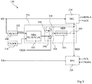
- the figure 5 represents, by schematic timing diagrams, an example of operation of the circuit of the figure 4 . More specifically, the figure 5 represents timing diagrams of an example of the signal RX, of the signal SYNC, of the values V410 of the content considered of the register 410, and of the measurement value STEP, as a function of time t.
- the RX signal presents a first falling edge, then a dominant state (D o ) with a duration of one bit, then a recessive state (R) with a duration of two bits which ends with a second falling edge.
- the SYNC signal has a logic high level for one clock cycle after detection of each of the falling edges.
- the SYNC signal has a low logic level when no falling edge is detected.
- the values V410 of the content of register 410 are in signed representation, that is to say that the most significant bit of the content considered corresponds to the bit of sign.
- the values of register 410 can also be in unsigned representation. In the example described above of a twenty-bit register 410 and a content formed of the 16 least significant bits, the value of bit number 15 (starting with 0 from the most significant bit low) corresponds to the sign bit.
- the AND logic gate 405 makes it possible to use the same circuit 336 to hold the stored value MES fixed during the sending of data and during the determination of the measurement value apart from the reception of the edges.
- the V410 value increases due to the addition of the STEP step every clock cycle.
- the increase is represented very schematically without showing the successive additions.
- the value V410 scans a range of values 510 several times. The time taken to scan the range of values 510 once is representative of the result of dividing the duration TCAN by the STEP step.
- the step STEP representing the measurement value of the TCLK/TCAN ratio
- the value STEPO is preferably that for which the value V410 scans the range of values 510 exactly once during the one-bit duration TCAN. Indeed, the ratio between the value STEPO and the extent of the range 510 is then equal to the ratio that there really is, in operation, between the cycle time TCLK of the clock 310 and the duration TCAN.
- the STEPO value may correspond to scanning the range exactly an integer number of times. Scanning can also be performed in the other direction than that shown, the STEPO value being negative.
- the V410 value did not scan the 510 range exactly three times during the three bit duration between the receipt of the first edge and the receipt of the second edge. More precisely, at the second edge, a value 520-2 of the sum of the step STEP and the value V410 during the clock cycle preceding the reset, has a result different from zero, here a negative value.
- the value 520-2 corresponds to the accumulation of a difference, for the clock cycles between the first and second edges, between the step STEP and the value STEPO.
- the difference is an algebraic value, that is to say it can be positive or negative.
- a value 520-1 corresponding to the accumulation of the difference during the time separating a preceding edge, not represented, and the first edge has also been represented.
- the AND logic gate 405 commands the stopping of the maintenance of the value stored in the circuit 334.
- the stored value is replaced by the value that the adder circuit 450 provides.
- the value supplied by circuit 440 has the opposite sign to that of value 520-1, 520-2 received by circuit 440.
- circuit 450 subtracts at step STEP an algebraic value 530-1, 530-2 representative of the value 520-1, 520-2.
- circuit 450 is replaced by a subtractor circuit.
- the value 530-1, 530-2 has the same sign as the respective value 520-1, 520-2. More specifically, the value 530-1, 530-2 provided by circuit 440 corresponds to the sum 520-1, 520-2, multiplied by a chosen constant small enough so that the removal of the value 530-1, 530-2 decreases, in absolute value, the difference between the STEP step and the STEPO value. In particular, circuit 440 is provided so that this constant decreases the difference between the step STEP and the value STEPO when the first and second edges are separated by a duration less than or equal to that of 10 times the TCAN duration of a bit. An example of such operation of circuit 440 is described below in connection with the figure 9 .
- a CAN bus frame includes at least one falling edge every 10 bits, this makes it possible to gradually bring the step STEP closer to the value STEPO, as shown. In other words, this makes it possible to gradually bring the measured value of the TCLK/TCAN ratio closer to the real value of the TCLK/TCAN ratio.
- the circuit of the figure 4 makes it easy to determine the measurement value without knowing in advance and/or without measuring the whole number of durations separating the consecutive falling edges.
- the circuit of the figure 4 is more robust to possible disturbances causing, for example, spurious edges or shifts in the instants at which the edges are detected.
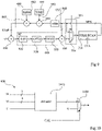
- the figure 6 schematically represents an embodiment of the encoding circuit 220 of the device of the picture 3 .
- the figure 7 represents, by schematic timing diagrams, the operation of the circuit of the figure 6 .
- the encoding circuit 220 takes up identical or similar circuits to the reset circuit 420, to the register 410, to the adder circuit 430 and to the calculation circuit 460 (CU), of the circuit 330 of the figure 4 , except that the reset circuit 420 is controlled by a signal TXSTART.
- the TXSTART signal commands the zeroing of register 410 by circuit 420 during one clock cycle at the start of sending a data frame.
- Reset circuit 420, register 410, adder circuit 430, and/or calculation circuit 460 may be separate from circuit 330, or, as in the preferred embodiment of figure 8 below, common with those of circuit 330.
- the value V410 of the contents of the register as a function of time t is represented schematically in figure 7 .
- the encoding circuit 220 further comprises a circuit 610 (MSBCHG?) connected, preferably connected, to the output (Q) of the register 410.
- the circuit 610 detects the crossing of a threshold by the contents of the register 410.
- this crossing corresponds to a change in value of one of the most significant bits MSB (“Most Significant Bits”) of the register.
- MSB Most Significant Bits
- the threshold thus corresponds, in this example, to a zero value of the content considered.
- any threshold value can be used, chosen as a function of the synchronization and/or of a duration between the reset command by the signal TXSTART and the sending of the frame.
- a crossing occurs each time the range 510 is scanned by the value V410 of the content considered, the consecutive crossings are separated by the duration of the range sweep.
- Circuit 610 provides a TXCLK signal on its output 612.
- An example of a TXCLK signal is represented schematically as a function of time t in figure 7 .
- the signal TXCLK takes on a first logic level, for example a high level, and remains at a low level when no signal is detected.
- the signal TXCLK can consist of any signal making it possible to transmit information on a threshold crossing by the contents of register 410.
- the circuit 220 further comprises a circuit 620 (FENC) receiving the data TDATA.
- the circuit 620 supplies at its output 622 a TXF frame formed from the TDATA data, ie encodes the TDATA data in the form of the TXF frame.
- Circuit 220 further comprises a serializer circuit 630 (SER) linked, preferably connected, to outputs 612 and 622.
- Circuit 630 receives frame TXF and serializes the data, synchronized by signal TXCLK.
- Circuit 630 provides the TX signal, shown as figure 7 , corresponding to applications of recessive (R) and dominant (D o ) levels to the bus in the order of the bits of the TXF frame. Each bit has the duration of the 510 range scan.
- the sending of the bits sent has thus been synchronized with respect to the duration TCAN of the bits previously received.
- the preferred case where device 130 is a slave device and can only send data after receiving a frame from master device 120 ( figure 1 ) makes it possible to ensure that data has indeed been received by the device 130 before sending the data.
- the time between, on the one hand, the end of the reception of the data frame coming from the master device allowing the sending of the data by the slave device, and, on the other hand, the beginning of the sending of the frame sent by the slave device is less than 100 times the TCAN duration, more preferably less than 20 times the TCAN duration. This makes it possible to ensure that variations in the cycle time between the measurement of the TCLK/TCAN ratio and the use of the measurement value of this ratio remain sufficiently small for the synchronization to be sufficient to ensure the correct reception of the data sent.
- circuit 800 schematically represents an embodiment of a circuit 800 of the device of the picture 3 . More specifically, circuit 800 includes a circuit 330 identical or similar to circuit 330 of the figure 4 , and a circuit 220 identical or similar to circuit 220 of the figure 6 , in which the reset circuits 420, the register 410, the adder circuit 430 and the calculation circuit 460 (CU) are common to the circuits 330 and 220.
- CU calculation circuit 460
- the circuit 800 comprises an AND logic gate 810 receiving, on an inverting input, the signal TXEN.
- the AND logic gate 810 receives, on a non-inverting input, the SYNC signal.
- An OR logic gate 820 has an input receiving the TXSTART signal and an input connected, preferably connected, to the output of the AND logic gate 810.
- the reset circuit 420 is connected, preferably connected, to the output of the OR logic gate 820.
- OR logic gate 820 provides the control signal for reset circuit 420.
- the logic circuit 840 consisting of the AND 810 and OR 820 logic gates thus makes it possible to control the resetting of the register 410 when the signal TXSTART corresponds to the start of a sending of a frame on the bus, and to control the resetting to zero of the register 410. zero of register 410 when the signal SYNC corresponds to the detection of a falling edge and the signal TXEN does not correspond to sending of a frame in progress.
- the logic circuit 840 thus allows the register 410 to be common for the sending of the frames and for the determination of the measurement value of the TCLK/TCAN ratio.
- An advantage of the present embodiment then is that circuit 800 includes fewer components, is more compact, and uses less area than embodiments in which circuits 220 and 330 do not have their components in common.
- Circuit 830 provides, on output 832, a high level when the number of scans of the value range of the content of register 410, considered to determine the measurement value and to send the data, is less than or equal to ten.
- the number of scans of the value range of the content of register 410 considered to determine the measurement value and to send the data, is less than or equal to ten.
- the four most significant bits correspond to this number of scans. In order to determine the measurement value, this ensures that falling edges received separated by more than ten bits are not taken into account.
- the figure 9 schematically represents an embodiment of a circuit of the device of the picture 3 . More precisely, the circuit represented in figure 9 corresponds to a part of a circuit 330 similar or identical to that of the figure 4 , including adder circuits 430 and 450, hold circuit 336, store circuit 314, and particular embodiments of circuits 440 (SC) and 460 (CU).
- the storage circuit 314 is, according to the present embodiment, constituted by a register, for example of eighteen bits.
- Calculation circuit 460 preferably includes a circuit 940 (MSB) for extracting most significant bits from register 314.
- circuit 940 extracts the nine most significant bits.
- Circuit 940 is optional, however, compared to an embodiment in which this circuit would be omitted, circuit 940 allows the number of bits in register 410 to be reduced while maintaining an accurate stored value.
- the calculation circuit 460 preferably comprises a circuit 965 for adding a predefined value 960, or constant value.
- the predefined value 960 is more preferably equal to 0x800, that is to say 32 times smaller than the range 0x10000 of the range scanned by the contents of register 410 used to determine the measurement value.
- the value 960 can be chosen in a similar way for other values of the ratio between the duration TCAN and the cycle time TCLK.
- the circuit 460 for calculating the step STEP from the stored value MES adds the predefined value 960 to the stored value. Compared to embodiments in which the circuit 965 is omitted, this makes it easier to obtain a starting value of the step STEP close to the real value STEPO of the ratio TCLK/TCAN.
- the circuit 965 can be replaced by an initialization circuit at a non-zero value of the stored value MES.
- Calculation circuit 460 preferably comprises an adder circuit 955 connected, preferably connected, to an output 952 of a circuit 950 (TEMP).
- the circuit 950 provides on its output 952 a calculated value as a function of the temperature of the device 130.
- the calculated value corresponds to a difference between the TCLK/TCAN ratio at the operating temperature of the device 130 and the TCLK/TCAN ratio at a temperature reference.
- Adder circuit 955 may have its output connected to the input of circuit 965, as shown. Circuit 955 thus adds a value calculated by circuit 950 to the stored value MES, preferably to the most significant bits of the stored value. As a variant, the adder circuits 955 and 965 can be exchanged, the adder circuit 955 then adding the value supplied by the circuit 950 to the sum of the value 960 and the most significant bits of the stored value.
- the circuit 460 for calculating the step STEP from the stored value MES adds to the stored value the value provided by the circuit 950.
- this allows the measurement value to remain closer to the real value of the TCLK/TCAN ratio when the temperature varies, in particular in the absence of reception of fronts and/or during the sending of data frames.
- the figure 10 schematically represents an embodiment of the circuit 950 of the circuit of the figure 9 .
- circuit 950 comprises a circuit 1010 (INTERP) receiving a measured temperature value T, three temperature values Ti and three values Vi associated respectively with the values Ti.
- circuit 1010 receives three predefined pairs each comprising one of the values Ti and the associated or corresponding value Vi.
- the associated value Vi constitutes for example the value calculated by the circuit 950 when the measured temperature T is equal to the value Ti.
- the circuit 1010 performs an interpolation, more preferably linear, from the values Ti and Vi.
- the number of pairs of values Ti and Vi can take any integer value greater than two, and the value calculated by the circuit 950 can then be extrapolated in any usual way from the pairs.
- the output of circuit 1010 is connected to adder circuit 955 via a multiplexer 1020.
- the multiplexer has an input (0) connected, preferably connected, to the output of interpolator circuit 1010.
- the multiplexer has a other input (1) receiving a null value.
- the multiplexer 1020 has its output connected, preferably connected, to the adder circuit 955.
- the multiplexer 1020 is controlled by a signal CAL. The multiplexer makes it possible, when the signal CAL commands the selection of the input to receive the zero value, to use the device to obtain the values Vi from the measurement values of the TCLK/TCAN ratio, without using the circuit 1010. thus calibrated the Vi values. After calibration, the values Vi can then be supplied to the circuit 1010.
- the figure 11 schematically represents an embodiment of the decoding circuit 210 of the device of the picture 3 .
- the decoding circuit 210 takes up identical or similar circuits to the reset circuits 420, to the register 410, to the adder circuit 430 of the circuit 330 of the figure 4 .
- the reset circuit 420, the register 410, the adder circuit 430, and/or the calculation circuit 460 can be distinct from those of the circuit 330, or preferably, common with those of the circuit 330.
- the register 410 has a content representing all or part of the register 410, this content repeatedly scanning a range of values in a manner similar to that described in connection with the figure 5 using the measurement value.
- the decoding circuit 210 preferably comprises a circuit 1110 (MdB) connected, preferably connected, to the Q output of the register 410.
- the circuit 1110 extracts most significant bits from the content of the register 410 preferably consisting of the 16 bits least significant of the register 410 of twenty bits. Preferably, the circuit extracts five bits, these bits more preferably having the numbers 11 to 15. The digital value corresponding to the extracted bits is provided on an output 1112 of the circuit 1110.
- the decoding circuit 210 comprises a circuit 1120 (>TH?) connected, preferably connected, to the output 1112 of the circuit 1110.
- the circuit 1120 detects the crossing of a threshold TH by the contents of the register 410.
- the circuit detects the crossing of the threshold TH by the value supplied by the circuit 1110.
- the threshold TH is chosen so that the crossing of the threshold occurs after the start of each sweep by the value V410 ( figure 5 ) of the contents of register 410 with a given delay between the start and the instant crossing the threshold.
- Circuit 1120 provides, on its output 1122, a threshold crossing detection signal.
- the decoding circuit 210 comprises a circuit 1130 (READ) receiving the signal RX and having an input 1131 linked, preferably connected, to the output 1122.
- the circuit 1130 reads the logic level of the signal RX on each crossing of the threshold TH by the V410 value.
- the circuit 1130 supplies the value read, corresponding to an RBIT bit, on its output 1132.
- the RBIT bits are preferably those of a frame comprising the falling edges making it possible to determine the measurement value.
- the decoding circuit 210 further comprises a frame decoder circuit 1140 (FDEC).
- the circuit 220 extracts the data RDATA from the succession of bits RBIT of the frame. The measurement value of the TCLK/TCAN ratio was thus used to receive the data. This results in a better synchronization of data reception than if the measured value was not used.
- the decoding circuit 210 preferably comprises a circuit 1150 (MSB) connected, preferably connected, to the Q output of the register 410.
- the circuit 1150 extracts most significant bits from the register, preferably bits different from those of the content used to determine the measurement value of the TCLK/TCAN ratio.
- the extracted bits correspond to the four most significant bits of the twenty-bit register 410. These bits represent an integer number increased by 1 with each scan of the range of values by the content of the least significant bits. In other words, these bits count the number of scans since the start of the frame, and this number corresponds to the position of the received bit in the frame.
- the position of the bit is provided by circuit 1150 on its output 1152.
- the circuit 1160 compares the position of the bit received in the frame with a predefined value. When position and value are equal, circuit 1160 issues an ACK-EN signal.
- the ACK-EN signal is for example used with the TXCLK signal ( figure 7 ) to obtain an ACK to be sent on the bus by circuit 220 ( picture 2 ).
- the measurement value of the TCLK/TCAN ratio was thus used to send the acknowledgment of receipt ACK. This results in better synchronization than if the acknowledgment was sent without using this value.
- circuit 1130 includes flip-flops synchronized by clock signal CLK, not shown.
- Circuit 1130 comprises three successive flip-flops 1210, 1215, 1222 in series, flip-flop 1210 receiving the RX signal on its D input.
- Flip-flop 1220 has its Q output connected by an inverter 1225 to an input of an OR logic gate 1230.
- Logic OR gate 1230 has another input connected, preferably connected, to the Q output of flip-flop 1215 and to the input of flip-flop 1220.
- the output of OR gate 1230 is connected, preferably connected, to an input of an AND logic gate 1235.
- the AND logic gate 1235 has a non-inverting input connected, preferably connected, to the output 1132 of the circuit 1130.
- the flip-flops 1210, 1215, 1220, the inverter 1225, and logic gates 1230 and 1235 are common with edge detection circuit 320 ( picture 3 ), the SYNC signal being supplied by the AND logic gate 1235.
- circuit 320 also supplies a signal TRIG.
- the TRIG signal is provided by the OR logic gate 1230 in this embodiment.
- the signal TRIG is preferably used combined with the clock signal CLK to control the scanning of the range of values by the register 410 only when receiving and sending data. This advantageously avoids part of the energy consumption by the register 410 apart from sending and receiving data.
- Circuit 1130 further comprises a flip-flop 1250 whose D input is linked, preferably connected, to input 1131 of circuit 1130.
- Output Q of flip-flop 1250 is linked, preferably connected, to an input of a AND logic gate 1260 through an inverter 1255.
- Circuit 1130 further includes an AND logic gate 1240 having an inverting input connected, preferably connected, to the output of logic gate 1235, and a non-inverting input connected, preferably connected, to the output of logic gate 1260.
- a multiplexer 1270 has a control input connected, preferably connected, to the output of the AND logic gate 1240.
- the multiplexer 1270 has a first input (1) connected, preferably connected, to the output of the flip-flop 1215. The first input is selected when the output of the AND logic gate 1240 is at a high logic level.
- Multiplexer 1270 has a second input (0) connected, preferably connected, to output 1132 of circuit 1130. The second input is selected when the output of AND logic gate 1240 is at a low logic level.
- Circuit 1130 further includes a flip-flop 1275 having its D input connected, preferably connected, to the output of multiplexer 1270. The Q output of flip-flop 1275 is connected, preferably connected, to output 1132 of circuit 1130.
- circuit 1140 ( figure 11 ) has an input connected, preferably connected, to the output of logic gate 1240.
- logic gate 1240 provides an OKDATA signal, received by circuit 1140, indicating to circuit 1140 that an RBIT bit is available at the output 1132 of circuit 1130.
- the figure 13 represents, partially and schematically, an example of an embodiment, according to a second aspect, of a device 130 constituting a circuit intended to be connected to a CAN bus.
- Circuit 130 is configured to have a sleep state and an awake state.
- the sleep state is defined by a state in which the power consumption by the circuit 130 is relatively low
- the waking state is defined by a state in which the power consumption by the circuit 130 is relatively high.
- the sleep state is obtained by reducing the activity, or by stopping the operation of at least a part of the circuits of the device 130. This makes it possible to reduce the electrical consumption compared to a device always in the waking state.
- Circuit 130 includes a clock 310 (CLOCK), similar to that described in connection with the figure 4 .
- the clock is stopped in the sleep state of the device. The clock therefore does not produce a CLK signal, or the CLK signal remains at the same logic level during the sleep state.
- the circuit 130 further comprises a circuit 1310 (WUFDET) for detecting a wake-up frame WUP ("wake up frame").
- Circuit 1310 receives clock signal CLK.
- Circuit 1310 emits a wake-up signal AWAKE when it has detected, that is to say recognized, the wake-up frame. The signal wake triggers the device to switch from the sleep state to the wake state.
- circuit 1310 has an input connected, preferably connected, to the output 1132 of a circuit 1130 (READ), as described in connection with the figure 11 , which receives the RX signal and provides the successive RBIT bits of the frame.
- RX circuit 1130
- the circuit 130 comprises a circuit for determining a measurement value of the TCLK/TCAN ratio, according to the first aspect ( figures 3 to 12 ).
- the measurement value is preferably used, as described in connection with the first aspect, to receive the RBIT bits of the frame.
- the circuit 1130 can use, for example on its input 1131 ( figure 12 ), any signal making it possible to define instants of reception of the bits by the circuit 1130.
- the circuit 1310 receives the signal RX directly and is configured to detect the wake-up frame WUP directly from the signal RX.
- the use of the measurement value of the TCLK/TCAN ratio makes it possible to synchronize the reception of the wake-up frame and improves its detection.
- Circuit 130 includes circuit 1320 receiving the RX signal.
- Circuit 1320 is a circuit for detecting edges 1320 (FEDET), preferably falling edges, in the RX signal.
- the edge detection circuit 320 corresponds to that described in relation to the picture 3 .
- edge detection circuit 1320 allows detection of edges without using the clock signal CLK, and may be separate from circuit 320. This allows edges to be detected when the device is in the sleep state.
- Circuit 1320 then has an output connected, preferably connected, to an input of clock CLK.
- circuit 1320 sends a signal to clock 310, and clock 310 is configured to start upon receipt of this signal.
- signal CLK is used by circuit 1310 to detect whether the detected edge belongs to a wake-up frame.
- the CLK signal is additionally used to determine the measurement value of the TCLK/TCAN ratio.
- circuit 130 further includes circuit 1140 (FDEC), as described in connection with figure 11 , decoding successive RBIT bits of the frame, to produce data. More preferably, circuit 1140 does not operate when the device is in the sleep state. The circuit 1140 then receives the wake-up signal AWAKE, and the reception of this signal causes the start of the circuit FDEC. Circuit 130 can then send data.
- This embodiment can also be combined with the embodiments according to the first aspect of the encoding circuit 220 and of the circuits 1150 and 1160 ( figure 11 ) sending an acknowledgment of receipt.
- the figure 14 represents, by schematic timing diagrams, an implementation mode step of a method of communication by a CAN bus to which the device of the figure 13 .
- the dominant (D o ) and recessive (R) states of the WUP wake-up frame are represented as a function of time.
- the instants at which the clock started and supplies the signal CLK have also been represented by hatching.
- the WUP frame is applied to the bus by a device connected to the bus, preferably the master device 120.
- the WUP frame is preferably intended to trigger the transition from the sleep state to the wake state of all the circuits 130 which are the sleep state before sending the frame.
- the WUP frame is conveyed by the bus and reaches the circuits 130 connected to the bus.
- the WUP wake-up frame comprises at least two consecutive cycles 1410 each consisting of a dominant state 1420 followed by a recessive state 1430.
- consecutive it is meant that the same edge 1415 corresponds to the end of a cycle 1410 and beginning of the next 1410 cycle.
- Each cycle consecutively has a single dominant 1420 state and a single recessive 1430 state. a data bit transported by the serial bus.
- the duration of each of the recessive 1430 and dominant 1420 states is greater than or equal to 1.8 ⁇ s.
- the duration of a dominant state corresponds to the time between a falling edge at the start of this dominant state, and a rising edge at the end of this dominant state.
- the duration of a recessive state corresponds to the time between a rising edge at the start of this recessive state, and a falling edge at the end of this recessive state.
- the start of the cycle 1410 arriving first in the WUP frame corresponds to a falling edge 1445 of the end of a recessive state 1440 preceding this first cycle.
- the end of the cycle arriving last in the frame corresponds to a falling edge 1455 of the start of a dominant state 1450 following this last cycle.
- the recessive 1430 and dominant 1420 states all have the same duration.
- the 1440 recessive state may have a different duration than the 1430 recessive and 1420 dominant states of the 1410 cycles.
- the 1450 dominant state may have a different duration than the 1430 recessive and 1420 dominant states of the 1410 cycles.
- the wake-up frame WUP thus forms at least three falling edges, namely the edges 1445, 1455, and at least one edge 1415. These falling edges are regularly alternated with at least two rising edges 1465 each between the dominant and recessive states of one of the 1410 cycles.
- the 1410 cycles are preceded by a period 1470 of transmitting start bits of the frame, the 1410 cycles then being located in the frame at data bit positions.
- the WUP frame includes at least one falling edge 1475 following another recessive state 1472 of period 1470.
- the falling edge 1475 is detected by circuit 1320 ( figure 13 ), which triggers the start of the clock 310 from a time t0.
- the clock 310 takes time to start.
- the CLK signal is provided by the clock 310 only from a time t1.
- Circuit 1310 ( figure 12 ) is able to detect the dominant and recessive states of the frame only from time t1.
- Time t1 may be located after the start of the 1410 cycles, and the 1310 circuit is then not able to recognize part of the recessive 1430 and dominant 1420 states of the 1410 cycles.
- the circuit 1310 can recognize at least part of the dominant 1430 and recessive 1420 states of the cycles of the frame, and trigger the awakening of circuit 130.
- the WUP wake-up frame comprising several 1410 cycles allows the clock 310 to be simpler, and simpler to manufacture, for example formed in and on a semiconductor substrate.
- the WUP frame can consist of only two 1410 cycles. However, depending on of the chosen clock and its starting time, it may be preferred that the frame comprise three or more than three consecutive cycles 1410, for example four or more than four consecutive cycles, preferentially five or more than five consecutive cycles.
- the measurement value can advantageously be determined during the cycles 1410 following the instant t1 of the start of the signal CLK.
- the number of consecutive cycles of the frame can be chosen so that the determination of the measurement value can be made between time t1 and the end of the WUP frame.
- the circuit 130 comprises a circuit 220 using the measurement value to send data
- the circuit 130 is, from the end of the wake-up frame WUP, advantageously ready to send data synchronized with respect to the duration TCAN.
- the circuit can also send a synchronized acknowledgment of the WUP frame.
Landscapes
- Engineering & Computer Science (AREA)
- Theoretical Computer Science (AREA)
- Physics & Mathematics (AREA)
- General Physics & Mathematics (AREA)
- General Engineering & Computer Science (AREA)
- Software Systems (AREA)
- Signal Processing (AREA)
- Computer Networks & Wireless Communication (AREA)
- Quality & Reliability (AREA)
- Computing Systems (AREA)
- Computer Security & Cryptography (AREA)
- Dc Digital Transmission (AREA)
- Information Transfer Systems (AREA)
- Synchronisation In Digital Transmission Systems (AREA)
- Small-Scale Networks (AREA)
Claims (16)
- Ein Verfahren, das die folgenden Schritte aufweist:- Empfangen von Flanken, die durch einen seriellen Bus (110) übertragen werden und durch Vielfache einer gleichen Dauer (TCAN) getrennt sind;- Bestimmen eines Messwertes (MES; STEP) eines Verhältnisses (TCLK/TCAN) zwischen einer Zykluszeit (TCLK) eines Taktgebers (310) und der Dauer (TCAN); und- Senden von Bits auf dem seriellen Bus (110) unter Verwendung des Messwerts (MES; STEP).
- Das Verfahren nach Anspruch 1, wobei der Empfang der Flanken vor dem Senden der Bits erfolgt.
- Das Verfahren nach Anspruch 1 oder 2, das den Empfang von Daten unter Verwendung des Messwerts (MES; STEP) aufweist, wobei die Flanken Flanken zwischen Bits der empfangenen Daten aufweisen.
- Das Verfahren nach Anspruch 3, das das Senden einer Empfangsbestätigung (ACK) für die Daten unter Verwendung des Messwerts (MES; STEP) aufweist.
- Das Verfahren nach einem der Ansprüche 1 bis 4, wobei die Bestimmung des Messwertes (MES; STEP) die Verwendung eines gespeicherten Wertes (MES) aufweist, der vorzugsweise während des Sendens der Bits fest gehalten wird.
- Das Verfahren nach Anspruch 5, wobei die Bestimmung des Messwertes (STEP) die Addition eines vorgegebenen Wertes (960) und/oder eines in Abhängigkeit von einer Temperatur (T) berechneten Wertes zu dem gespeicherten Wert (MES) aufweist.
- Das Verfahren nach Anspruch 6, wobei der berechnete Wert aus einer Vielzahl von vordefinierten Paaren extrapoliert wird, die jeweils einen Temperaturwert (Ti) und einen dem berechneten Wert (Vi) entsprechenden Wert für den Temperaturwert (Ti) aufweisen.
- Das Verfahren nach einem der Ansprüche 5 bis 7, wobei die Bestimmung des Messwertes (STEP) Folgendes aufweist:- die Bestimmung eines ersten Wertes (530-1, 530-2), der repräsentativ ist für eine Summe von Differenzen zwischen dem Messwert (STEP) und einem tatsächlichen Wert (STEPO) des Verhältnisses (TCLK/TCAN) für die Zyklen des Taktgebers (310), die zwischen dem Empfang von zwei der Flanken vorhanden sind; und- die Subtraktion des ersten repräsentativen Wertes (530-1, 530-2) von dem gespeicherten Wert (MES).
- Das Verfahren nach Anspruch 8, aufweisend bei jedem Zyklus des Taktgebers (310) die ganzzahlige Modulo-Addition eines zweiten Wertes, der für den Messwert (STEP) repräsentativ ist, zum Inhalt eines Registers (410), wobei die Bestimmung des ersten repräsentativen Wertes (530-1, 530-2) auf einer Differenz des Inhalts des Registers (410) zwischen den Empfangszeiten der beiden Flanken basiert.
- Das Verfahren nach Anspruch 9, wobei das Senden jedes der Bits zu einem Zeitpunkt beginnt, zu dem der Inhalt des Registers (410) einen Schwellenwert überschreitet.
- Das Verfahren nach einem der Ansprüche 5 bis 10, wobei das Festhalten des gespeicherten Wertes (MES) durch einen Multiplexer (338) implementiert wird, der den gespeicherten Wert bereitstellt, wobei ein Eingang unter einer Vielzahl von Eingängen des Multiplexers den gespeicherten Wert (MES) empfängt, wobei der Eingang unter einer Vielzahl von Eingängen während des Sendens der Bits ausgewählt wird.
- Eine Vorrichtung (130), die konfiguriert ist, um das Verfahren nach einem der Ansprüche 1 bis 10 zu implementieren.
- Die Vorrichtung (130) nach Anspruch 12, die dazu bestimmt ist, mit dem seriellen Bus (110) verbunden zu werden, und die den Taktgeber (310) aufweist, wobei der Taktgeber (310) vorzugsweise in und auf einem Halbleitersubstrat angeordnet ist.
- Die Vorrichtung nach Anspruch 12 oder 13, die so konfiguriert ist, dass sie einen Schlafzustand und einen Wachzustand hat, und damit ein Übergang vom Schlafzustand in den Wachzustand durch einen vom seriellen Bus (110) übertragenen Rahmen (WUP) ausgelöst wird, wobei der Rahmen mindestens zwei aufeinanderfolgende Zyklen (1410) eines dominanten Zustands (1420) aufweist, auf den ein rezessiver Zustand (1430) folgt, wobei die rezessiven Zustände (1430) und die dominanten Zustände (1420) weitere Dauern haben, die zwischen dem 2-und 5-fachen der Dauer liegen.
- Ein System (100), das einen seriellen Bus (110) und eine oder mehrere erste Vorrichtungen (130) nach einem der Ansprüche 12 bis 14 aufweist, die mit dem seriellen Bus gekoppelt sind.
- Das System nach Anspruch 15, das eine mit dem seriellen Bus gekoppelte zweite Vorrichtung (120) aufweist, die konfiguriert ist, Folgendes zu senden:- erste Nachrichten, die einen Satz von Operationen enthalten, die von den ersten Vorrichtungen (130) implementiert werden sollen; und- zweite Nachrichten, die an einen Teil der ersten Vorrichtungen (130) adressiert sind, wobei die zweiten Nachrichten jeweilige Kennungen der ersten Vorrichtungen (130) übermitteln, an die die zweiten Nachrichten jeweils adressiert sind, wobei die zweiten Nachrichten von den ersten Vorrichtungen (130), an die sie adressiert sind, anfordern, jeweilige Reaktionen an die zweite Vorrichtung (120) innerhalb jeweiliger erwarteter Zeitintervalle zu senden,wobei die ersten Vorrichtungen (130) konfiguriert sind, zum:- Empfangen der ersten Nachrichten, Lesen des Satzes von zu implementierenden Operationen und Implementieren von Operationen in Abhängigkeit von dem gelesenen Satz; und- Empfangen der zweiten Nachrichten und Reagieren auf die zweiten Nachrichten durch Senden von Reaktionen an die zweite Vorrichtung (120) innerhalb der jeweiligen erwarteten Zeitintervalle.
Applications Claiming Priority (1)
| Application Number | Priority Date | Filing Date | Title |
|---|---|---|---|
| FR1909968A FR3100629B1 (fr) | 2019-09-10 | 2019-09-10 | Communication par bus CAN |
Publications (2)
| Publication Number | Publication Date |
|---|---|
| EP3793142A1 EP3793142A1 (de) | 2021-03-17 |
| EP3793142B1 true EP3793142B1 (de) | 2022-10-26 |
Family
ID=69104629
Family Applications (1)
| Application Number | Title | Priority Date | Filing Date |
|---|---|---|---|
| EP20194698.5A Active EP3793142B1 (de) | 2019-09-10 | 2020-09-04 | Kommunikation über can-bus |
Country Status (4)
| Country | Link |
|---|---|
| US (2) | US11657017B2 (de) |
| EP (1) | EP3793142B1 (de) |
| CN (1) | CN112565033B (de) |
| FR (1) | FR3100629B1 (de) |
Families Citing this family (4)
| Publication number | Priority date | Publication date | Assignee | Title |
|---|---|---|---|---|
| FR3100628B1 (fr) | 2019-09-10 | 2023-04-14 | St Microelectronics Grenoble 2 | Communication par bus CAN |
| FR3102584B1 (fr) | 2019-10-28 | 2021-11-05 | St Microelectronics Grenoble 2 | Procédé d'acquittement de communication par bus |
| US20220358069A1 (en) * | 2021-05-07 | 2022-11-10 | Chronos Tech Llc | ADVANCED CENTRALIZED CHRONOS NoC |
| EP4138343B1 (de) * | 2021-08-20 | 2024-02-21 | STMicroelectronics Application GmbH | Verarbeitungssystem, zugehörige integrierte schaltung, vorrichtung und verfahren |
Family Cites Families (61)
| Publication number | Priority date | Publication date | Assignee | Title |
|---|---|---|---|---|
| DE3537477A1 (de) * | 1985-10-22 | 1987-04-23 | Porsche Ag | Anordnung zur individuellen anpassung einer seriellen schnittstelle eines datenverarbeitenden systems an eine datenuebertragungsgeschwindigkeit eines kommunikationspartners |
| CA1318969C (en) * | 1987-06-25 | 1993-06-08 | Shoji Mizuno | Encoding of a picture signal in consideration of contrast in each picture and decoding corresponding to the encoding |
| US5867695A (en) * | 1992-10-16 | 1999-02-02 | International Business Machines Corp. | Method and system for reduced metastability between devices which communicate and operate at different clock frequencies |
| US5327144A (en) * | 1993-05-07 | 1994-07-05 | Associated Rt, Inc. | Cellular telephone location system |
| JPH10303851A (ja) * | 1997-04-25 | 1998-11-13 | Mitsubishi Electric Corp | デジタル放送受信機 |
| FR2765706B1 (fr) * | 1997-07-04 | 1999-10-01 | Sgs Thomson Microelectronics | Lecteur de cartes a puces a protocole de transmission rapide |
| US5898640A (en) * | 1997-09-26 | 1999-04-27 | Advanced Micro Devices, Inc. | Even bus clock circuit |
| JP3610854B2 (ja) * | 1999-12-27 | 2005-01-19 | 株式会社日立製作所 | 情報処理装置および情報処理システム |
| US7042932B1 (en) * | 1999-12-28 | 2006-05-09 | Intel Corporation | Synchronization detection architecture for serial data communication |
| CN1173474C (zh) | 2000-03-25 | 2004-10-27 | 特克特朗尼克公司 | 数字相位分析器和合成器 |
| DE10102871C2 (de) * | 2001-01-23 | 2003-03-06 | Infineon Technologies Ag | Halbleiterbauelement zum Anschluß an ein Testsystem sowie Testsystem mit dem Halbleiterbauelement |
| US6677786B2 (en) * | 2001-02-28 | 2004-01-13 | Brecis Communications Corporation | Multi-service processor clocking system |
| DE60220863T2 (de) * | 2001-04-24 | 2008-03-13 | Rambus Inc., Los Altos | Verfahren und Gerät zum Koordinieren von Speicheroperationen zwischen unterschiedlich angeordneten Speicherkomponenten |
| US20020199124A1 (en) * | 2001-06-22 | 2002-12-26 | Adkisson Richard W. | System and method for synchronizing data transfer across a clock domain boundary |
| US7296174B2 (en) * | 2002-10-11 | 2007-11-13 | Broadcom Corporation | Apparatus and method to interface two different clock domains |
| KR100547831B1 (ko) * | 2003-06-18 | 2006-01-31 | 삼성전자주식회사 | 가변 데이터 전송률에 대응이 가능한 클럭 및 데이터 복원장치 |
| ATE392066T1 (de) * | 2004-05-03 | 2008-04-15 | Freescale Semiconductor Inc A | Verfahren und vorrichtung zur knotenaufwachung in einem serieller datenbus |
| US8018463B2 (en) * | 2004-05-10 | 2011-09-13 | Nvidia Corporation | Processor for video data |
| US7436917B2 (en) * | 2004-07-29 | 2008-10-14 | Hewlett-Packard Development Company, L.P. | Controller for clock synchronizer |
| US7391836B2 (en) * | 2005-03-23 | 2008-06-24 | Analog Devices, Inc. | System and method for synchronous clock re-generation from a non-synchronous interface |
| US7747901B2 (en) * | 2005-07-20 | 2010-06-29 | Texas Instruments Incorporated | Auxiliary link control commands |
| DE102006013640A1 (de) * | 2006-03-22 | 2007-09-27 | Robert Bosch Gmbh | Verfahren und Datenübertragungssystem zur Übergabe von Daten zwischen dem Datenübertragungssystem und einem Host-Prozessor eines Teilnehmers eines Datenübertragungssystems |
| US7496779B2 (en) * | 2006-06-13 | 2009-02-24 | Via Technologies, Inc. | Dynamically synchronizing a processor clock with the leading edge of a bus clock |
| US20090086874A1 (en) * | 2007-09-28 | 2009-04-02 | Junning Wang | Apparatus and method of elastic buffer control |
| US7921322B2 (en) * | 2007-10-17 | 2011-04-05 | Spansion Llc | Optimize personalization conditions for electronic device transmission rates with increased transmitting frequency |
| US8051320B2 (en) * | 2007-12-12 | 2011-11-01 | Mips Technologies, Inc. | Clock ratio controller for dynamic voltage and frequency scaled digital systems, and applications thereof |
| US7936637B2 (en) * | 2008-06-30 | 2011-05-03 | Micron Technology, Inc. | System and method for synchronizing asynchronous signals without external clock |
| US8391469B2 (en) * | 2008-07-11 | 2013-03-05 | Texas Instruments Incorporated | Methods and apparatus to decode dual-tone signals |
| US8041981B2 (en) * | 2008-09-25 | 2011-10-18 | Apple Inc. | Synchronizing timing domains based on state variables |
| US9098816B2 (en) * | 2009-01-14 | 2015-08-04 | GM Global Technology Operations LLC | Message loss prevention in can systems |
| CN101820324B (zh) * | 2010-04-30 | 2014-04-09 | 中兴通讯股份有限公司 | 一种异步数据的同步传输方法和系统 |
| KR20120011974A (ko) * | 2010-07-29 | 2012-02-09 | 삼성전자주식회사 | 복수 개의 인터페이스를 지원하는 스마트 카드 및 그것의 인터페이스 방법 |
| US8504864B2 (en) * | 2010-12-01 | 2013-08-06 | GM Global Technology Operations LLC | Data sensor coordination using time synchronization in a multi-bus controller area network system |
| US8798223B2 (en) * | 2010-12-23 | 2014-08-05 | Ashish K. Choudhury | Clock and data recovery unit without an external reference clock |
| JP5699759B2 (ja) * | 2011-04-01 | 2015-04-15 | 富士通株式会社 | 伝送装置及び伝送方法 |
| JP5912182B2 (ja) * | 2011-08-11 | 2016-04-27 | バルーフ ゲゼルシャフト ミット ベシュレンクテル ハフツング | 測定値送信装置 |
| TWI466522B (zh) * | 2011-10-21 | 2014-12-21 | Realtek Semiconductor Corp | 一種調整一傳送時脈之收發裝置以及相關方法 |
| CN103187925B (zh) * | 2011-12-31 | 2016-06-15 | 意法半导体研发(上海)有限公司 | 使用跟踪振荡器电路的hs-can总线时钟恢复 |
| EP2831603B1 (de) * | 2012-03-30 | 2019-11-13 | Intel Corporation | Volldigitale verzögerungsmessungsschaltung auf einem chip |
| KR20130113203A (ko) * | 2012-04-05 | 2013-10-15 | 삼성전자주식회사 | 전자 장치 및 전자 장치의 파워 관리 방법 |
| DE102012108696B4 (de) * | 2012-09-17 | 2020-08-06 | Wago Verwaltungsgesellschaft Mbh | Datenbusteilnehmer und Verfahren zur Synchronisation von Datenbusteilnehmern |
| US20160087737A1 (en) * | 2013-05-29 | 2016-03-24 | Freescale Semiconductor, Inc. | A network receiver for a network using distributed clock synchronization and a method of sampling a signal received from the network |
| US9524264B2 (en) * | 2014-06-26 | 2016-12-20 | Qualcomm Incorporated | Generating combined bus clock signals using asynchronous master device reference clocks in shared bus systems, and related methods, devices, and computer-readable media |
| KR102285789B1 (ko) * | 2014-07-01 | 2021-08-04 | 삼성전자 주식회사 | 외장 저장 장치, 및 이의 기준 주파수를 설정하는 방법 |
| US10013375B2 (en) * | 2014-08-04 | 2018-07-03 | Samsung Electronics Co., Ltd. | System-on-chip including asynchronous interface and driving method thereof |
| US9843597B2 (en) * | 2015-01-05 | 2017-12-12 | International Business Machines Corporation | Controller area network bus monitor |
| DE102015211667A1 (de) | 2015-06-24 | 2016-12-29 | Robert Bosch Gmbh | Ventil zum Zumessen eines Fluids |
| US10482045B2 (en) * | 2016-02-17 | 2019-11-19 | Analog Devices Global Unlimited Company | Data communication interface for processing data in low power systems |
| US10560252B2 (en) * | 2016-04-01 | 2020-02-11 | Intel Corporation | Time aware audio streams with heterogenous frame rates |
| US20170373881A1 (en) * | 2016-06-27 | 2017-12-28 | Qualcomm Incorporated | Systems and methods for controlling isochronous data streams |
| US10368174B2 (en) * | 2016-06-28 | 2019-07-30 | Semiconductor Components Industries, Llc | Distributed phase locked loop in hearing instruments |
| US9912468B1 (en) * | 2016-08-18 | 2018-03-06 | Keyssa Systems, Inc. | Multi-data rates multi-protocol communications techniques for reference-less re-timer |
| JP2018044884A (ja) * | 2016-09-15 | 2018-03-22 | ルネサスエレクトロニクス株式会社 | 温度計測回路、集積回路、及び温度計測方法 |
| KR102670999B1 (ko) * | 2016-12-28 | 2024-05-30 | 삼성전자주식회사 | Dvfs 동작을 수행하는 어플리케이션 프로세서, 이를 포함하는 컴퓨팅 시스템 및 이의 동작 방법 |
| US20190025872A1 (en) * | 2017-07-18 | 2019-01-24 | Qualcomm Incorporated | Usb device with clock domain correlation |
| KR102434989B1 (ko) * | 2017-12-05 | 2022-08-22 | 삼성전자주식회사 | 클록간 정렬을 위한 트레이닝을 수행하는 메모리 장치, 메모리 시스템 및 이의 동작 방법 |
| IT201800003980A1 (it) | 2018-03-26 | 2019-09-26 | Stmicroelectronics Application Gmbh | Procedimento di comunicazione, sistema, dispositivi, segnale e veicolo corrispondenti |
| DE102019201316A1 (de) * | 2019-02-01 | 2020-08-06 | Robert Bosch Gmbh | Teilnehmerstation für ein serielles Bussystem und Verfahren zur Kommunikation in einem seriellen Bussystem |
| JP2021029063A (ja) * | 2019-08-09 | 2021-02-25 | ミネベアミツミ株式会社 | Pwm信号測定装置、モータ駆動制御装置、pwm信号測定方法、およびモータ駆動制御方法 |
| FR3100628B1 (fr) * | 2019-09-10 | 2023-04-14 | St Microelectronics Grenoble 2 | Communication par bus CAN |
| CN110673524B (zh) * | 2019-09-27 | 2020-09-22 | 安凯(广州)微电子技术有限公司 | 一种高速spi主模式控制器 |
-
2019
- 2019-09-10 FR FR1909968A patent/FR3100629B1/fr active Active
-
2020
- 2020-09-02 US US17/009,903 patent/US11657017B2/en active Active
- 2020-09-04 EP EP20194698.5A patent/EP3793142B1/de active Active
- 2020-09-09 CN CN202010939720.XA patent/CN112565033B/zh active Active
-
2023
- 2023-05-02 US US18/310,864 patent/US12475074B2/en active Active
Also Published As
| Publication number | Publication date |
|---|---|
| FR3100629A1 (fr) | 2021-03-12 |
| US20210073167A1 (en) | 2021-03-11 |
| CN112565033A (zh) | 2021-03-26 |
| EP3793142A1 (de) | 2021-03-17 |
| US12475074B2 (en) | 2025-11-18 |
| US20230273896A1 (en) | 2023-08-31 |
| CN112565033B (zh) | 2023-02-14 |
| FR3100629B1 (fr) | 2023-04-07 |
| US11657017B2 (en) | 2023-05-23 |
Similar Documents
| Publication | Publication Date | Title |
|---|---|---|
| EP3793142B1 (de) | Kommunikation über can-bus | |
| EP0269481B1 (de) | Verfahren und Gerät zur Übertragung digitaler Daten | |
| EP3793132B1 (de) | Kommunikation über can-bus | |
| EP0466591A1 (de) | Verfahren und Anordnung für digitale serielle Datenübertragung | |
| FR3003417A1 (fr) | Systeme et procede de communication bas debit a courant porteur | |
| EP0621703B1 (de) | Verfahren und Vorrichtung zur Taktrückgewinnung und Synchronisierung für den Empfang über ein ATM-Netz übertragener Daten | |
| EP0459911A1 (de) | Verfahren zum Vermindern von Niederfrequenz-Zitterkomponenten in einem digitalen Daten-Übertragungssystem | |
| EP0056748B1 (de) | Verfahren zur empfangsseitigen Synchronisation paketweise übertragener, digitaler Signale | |
| EP0228528A1 (de) | Einrichtung zur Realisierung eines Kodes mit schwacher laufender Summe in schneller digitaler Übertragung und eine solche Einrichtung benutzendes Kodierungsverfahren | |
| FR2790892A1 (fr) | Procede et dispositif de controle de la synchronisation entre deux bus de communication serie d'un reseau | |
| EP0229738B1 (de) | Verfahren und Anordnung zur Regenration der Unversehrtheit eines binären Informationsflusses in einem pleisiochronen Netzwerk | |
| EP0982866B1 (de) | Verfahren zur Faltungskodierung und Uebertragung von digitalen Datenpaketen, Gerät und Verfahren zur entsprechenden Dekodierung | |
| FR2646742A1 (fr) | Dispositif pour synchroniser un signal pseudo-binaire avec un signal d'horloge regeneree a sauts de phase | |
| EP0717575A2 (de) | Funk-Kommunikationssystem mit verteilten Feststationen | |
| EP3387766B1 (de) | Verfahren und vorrichtungen zum senden eines kontinuierlichen bitstroms in einem nicht mit dem bitstrom synchronen digitalen netzwerk | |
| FR2793624A1 (fr) | Procede et dispositif de controle de la synchronisation entre deux noeuds d'un reseau | |
| FR2793623A1 (fr) | Procede et dispositif de controle de la synchronisation entre deux noeuds ni-1, ni d'un reseau | |
| FR2538647A1 (fr) | Circuit de demultiplexage d'un signal numerique en trames et a haut debit | |
| FR2736478A1 (fr) | Procedes et dispositifs de codage et de decodage d'informations binaires en impulsions de durees variables | |
| EP3816808A1 (de) | Verfahren zur kommunikationsbestätigung durch bus | |
| WO2008068394A1 (fr) | Procédé et systeme de transmission d'informations | |
| WO2006045943A1 (fr) | Procede de synchronisation d'un recepteur radio, et recepteur adapte pour mettre en œuvre un tel procede | |
| EP1245099A1 (de) | Vorrichtung zum empfang der datenpacketen | |
| FR2940874A1 (fr) | Procede de synchronisation d'une transmission de trames de donnees applicatives, dispositifs d'emission et de reception, produit programme d'ordinateur et moyen de stockage correspondants | |
| FR2877800A1 (fr) | Dispositif perfectionne de decodage, adapte a un systeme de transmission utilisant un etalement de spectre a sequence directe |
Legal Events
| Date | Code | Title | Description |
|---|---|---|---|
| PUAI | Public reference made under article 153(3) epc to a published international application that has entered the european phase |
Free format text: ORIGINAL CODE: 0009012 |
|
| STAA | Information on the status of an ep patent application or granted ep patent |
Free format text: STATUS: REQUEST FOR EXAMINATION WAS MADE |
|
| 17P | Request for examination filed |
Effective date: 20200904 |
|
| AK | Designated contracting states |
Kind code of ref document: A1 Designated state(s): AL AT BE BG CH CY CZ DE DK EE ES FI FR GB GR HR HU IE IS IT LI LT LU LV MC MK MT NL NO PL PT RO RS SE SI SK SM TR |
|
| AX | Request for extension of the european patent |
Extension state: BA ME |
|
| RIC1 | Information provided on ipc code assigned before grant |
Ipc: H04L 12/40 20060101AFI20220303BHEP |
|
| GRAP | Despatch of communication of intention to grant a patent |
Free format text: ORIGINAL CODE: EPIDOSNIGR1 |
|
| STAA | Information on the status of an ep patent application or granted ep patent |
Free format text: STATUS: GRANT OF PATENT IS INTENDED |
|
| INTG | Intention to grant announced |
Effective date: 20220408 |
|
| GRAS | Grant fee paid |
Free format text: ORIGINAL CODE: EPIDOSNIGR3 |
|
| GRAA | (expected) grant |
Free format text: ORIGINAL CODE: 0009210 |
|
| STAA | Information on the status of an ep patent application or granted ep patent |
Free format text: STATUS: THE PATENT HAS BEEN GRANTED |
|
| AK | Designated contracting states |
Kind code of ref document: B1 Designated state(s): AL AT BE BG CH CY CZ DE DK EE ES FI FR GB GR HR HU IE IS IT LI LT LU LV MC MK MT NL NO PL PT RO RS SE SI SK SM TR |
|
| REG | Reference to a national code |
Ref country code: GB Ref legal event code: FG4D Free format text: NOT ENGLISH |
|
| REG | Reference to a national code |
Ref country code: CH Ref legal event code: EP |
|
| REG | Reference to a national code |
Ref country code: AT Ref legal event code: REF Ref document number: 1527886 Country of ref document: AT Kind code of ref document: T Effective date: 20221115 |
|
| REG | Reference to a national code |
Ref country code: DE Ref legal event code: R096 Ref document number: 602020005853 Country of ref document: DE |
|
| REG | Reference to a national code |
Ref country code: IE Ref legal event code: FG4D Free format text: LANGUAGE OF EP DOCUMENT: FRENCH |
|
| REG | Reference to a national code |
Ref country code: LT Ref legal event code: MG9D |
|
| REG | Reference to a national code |
Ref country code: NL Ref legal event code: MP Effective date: 20221026 |
|
| REG | Reference to a national code |
Ref country code: AT Ref legal event code: MK05 Ref document number: 1527886 Country of ref document: AT Kind code of ref document: T Effective date: 20221026 |
|
| PG25 | Lapsed in a contracting state [announced via postgrant information from national office to epo] |
Ref country code: NL Free format text: LAPSE BECAUSE OF FAILURE TO SUBMIT A TRANSLATION OF THE DESCRIPTION OR TO PAY THE FEE WITHIN THE PRESCRIBED TIME-LIMIT Effective date: 20221026 |
|
| PG25 | Lapsed in a contracting state [announced via postgrant information from national office to epo] |
Ref country code: SE Free format text: LAPSE BECAUSE OF FAILURE TO SUBMIT A TRANSLATION OF THE DESCRIPTION OR TO PAY THE FEE WITHIN THE PRESCRIBED TIME-LIMIT Effective date: 20221026 Ref country code: PT Free format text: LAPSE BECAUSE OF FAILURE TO SUBMIT A TRANSLATION OF THE DESCRIPTION OR TO PAY THE FEE WITHIN THE PRESCRIBED TIME-LIMIT Effective date: 20230227 Ref country code: NO Free format text: LAPSE BECAUSE OF FAILURE TO SUBMIT A TRANSLATION OF THE DESCRIPTION OR TO PAY THE FEE WITHIN THE PRESCRIBED TIME-LIMIT Effective date: 20230126 Ref country code: LT Free format text: LAPSE BECAUSE OF FAILURE TO SUBMIT A TRANSLATION OF THE DESCRIPTION OR TO PAY THE FEE WITHIN THE PRESCRIBED TIME-LIMIT Effective date: 20221026 Ref country code: FI Free format text: LAPSE BECAUSE OF FAILURE TO SUBMIT A TRANSLATION OF THE DESCRIPTION OR TO PAY THE FEE WITHIN THE PRESCRIBED TIME-LIMIT Effective date: 20221026 Ref country code: ES Free format text: LAPSE BECAUSE OF FAILURE TO SUBMIT A TRANSLATION OF THE DESCRIPTION OR TO PAY THE FEE WITHIN THE PRESCRIBED TIME-LIMIT Effective date: 20221026 Ref country code: AT Free format text: LAPSE BECAUSE OF FAILURE TO SUBMIT A TRANSLATION OF THE DESCRIPTION OR TO PAY THE FEE WITHIN THE PRESCRIBED TIME-LIMIT Effective date: 20221026 |
|
| PG25 | Lapsed in a contracting state [announced via postgrant information from national office to epo] |
Ref country code: RS Free format text: LAPSE BECAUSE OF FAILURE TO SUBMIT A TRANSLATION OF THE DESCRIPTION OR TO PAY THE FEE WITHIN THE PRESCRIBED TIME-LIMIT Effective date: 20221026 Ref country code: PL Free format text: LAPSE BECAUSE OF FAILURE TO SUBMIT A TRANSLATION OF THE DESCRIPTION OR TO PAY THE FEE WITHIN THE PRESCRIBED TIME-LIMIT Effective date: 20221026 Ref country code: LV Free format text: LAPSE BECAUSE OF FAILURE TO SUBMIT A TRANSLATION OF THE DESCRIPTION OR TO PAY THE FEE WITHIN THE PRESCRIBED TIME-LIMIT Effective date: 20221026 Ref country code: IS Free format text: LAPSE BECAUSE OF FAILURE TO SUBMIT A TRANSLATION OF THE DESCRIPTION OR TO PAY THE FEE WITHIN THE PRESCRIBED TIME-LIMIT Effective date: 20230226 Ref country code: HR Free format text: LAPSE BECAUSE OF FAILURE TO SUBMIT A TRANSLATION OF THE DESCRIPTION OR TO PAY THE FEE WITHIN THE PRESCRIBED TIME-LIMIT Effective date: 20221026 Ref country code: GR Free format text: LAPSE BECAUSE OF FAILURE TO SUBMIT A TRANSLATION OF THE DESCRIPTION OR TO PAY THE FEE WITHIN THE PRESCRIBED TIME-LIMIT Effective date: 20230127 |
|
| REG | Reference to a national code |
Ref country code: DE Ref legal event code: R097 Ref document number: 602020005853 Country of ref document: DE |
|
| PG25 | Lapsed in a contracting state [announced via postgrant information from national office to epo] |
Ref country code: SM Free format text: LAPSE BECAUSE OF FAILURE TO SUBMIT A TRANSLATION OF THE DESCRIPTION OR TO PAY THE FEE WITHIN THE PRESCRIBED TIME-LIMIT Effective date: 20221026 Ref country code: RO Free format text: LAPSE BECAUSE OF FAILURE TO SUBMIT A TRANSLATION OF THE DESCRIPTION OR TO PAY THE FEE WITHIN THE PRESCRIBED TIME-LIMIT Effective date: 20221026 Ref country code: EE Free format text: LAPSE BECAUSE OF FAILURE TO SUBMIT A TRANSLATION OF THE DESCRIPTION OR TO PAY THE FEE WITHIN THE PRESCRIBED TIME-LIMIT Effective date: 20221026 Ref country code: DK Free format text: LAPSE BECAUSE OF FAILURE TO SUBMIT A TRANSLATION OF THE DESCRIPTION OR TO PAY THE FEE WITHIN THE PRESCRIBED TIME-LIMIT Effective date: 20221026 Ref country code: CZ Free format text: LAPSE BECAUSE OF FAILURE TO SUBMIT A TRANSLATION OF THE DESCRIPTION OR TO PAY THE FEE WITHIN THE PRESCRIBED TIME-LIMIT Effective date: 20221026 |
|
| PG25 | Lapsed in a contracting state [announced via postgrant information from national office to epo] |
Ref country code: SK Free format text: LAPSE BECAUSE OF FAILURE TO SUBMIT A TRANSLATION OF THE DESCRIPTION OR TO PAY THE FEE WITHIN THE PRESCRIBED TIME-LIMIT Effective date: 20221026 Ref country code: AL Free format text: LAPSE BECAUSE OF FAILURE TO SUBMIT A TRANSLATION OF THE DESCRIPTION OR TO PAY THE FEE WITHIN THE PRESCRIBED TIME-LIMIT Effective date: 20221026 |
|
| PLBE | No opposition filed within time limit |
Free format text: ORIGINAL CODE: 0009261 |
|
| STAA | Information on the status of an ep patent application or granted ep patent |
Free format text: STATUS: NO OPPOSITION FILED WITHIN TIME LIMIT |
|
| 26N | No opposition filed |
Effective date: 20230727 |
|
| PG25 | Lapsed in a contracting state [announced via postgrant information from national office to epo] |
Ref country code: SI Free format text: LAPSE BECAUSE OF FAILURE TO SUBMIT A TRANSLATION OF THE DESCRIPTION OR TO PAY THE FEE WITHIN THE PRESCRIBED TIME-LIMIT Effective date: 20221026 |
|
| REG | Reference to a national code |
Ref country code: CH Ref legal event code: PL |
|
| PG25 | Lapsed in a contracting state [announced via postgrant information from national office to epo] |
Ref country code: LU Free format text: LAPSE BECAUSE OF NON-PAYMENT OF DUE FEES Effective date: 20230904 |
|
| REG | Reference to a national code |
Ref country code: BE Ref legal event code: MM Effective date: 20230930 |
|
| PG25 | Lapsed in a contracting state [announced via postgrant information from national office to epo] |
Ref country code: LU Free format text: LAPSE BECAUSE OF NON-PAYMENT OF DUE FEES Effective date: 20230904 Ref country code: IT Free format text: LAPSE BECAUSE OF FAILURE TO SUBMIT A TRANSLATION OF THE DESCRIPTION OR TO PAY THE FEE WITHIN THE PRESCRIBED TIME-LIMIT Effective date: 20221026 Ref country code: MC Free format text: LAPSE BECAUSE OF FAILURE TO SUBMIT A TRANSLATION OF THE DESCRIPTION OR TO PAY THE FEE WITHIN THE PRESCRIBED TIME-LIMIT Effective date: 20221026 |
|
| REG | Reference to a national code |
Ref country code: IE Ref legal event code: MM4A |
|
| PG25 | Lapsed in a contracting state [announced via postgrant information from national office to epo] |
Ref country code: IE Free format text: LAPSE BECAUSE OF NON-PAYMENT OF DUE FEES Effective date: 20230904 |
|
| PG25 | Lapsed in a contracting state [announced via postgrant information from national office to epo] |
Ref country code: CH Free format text: LAPSE BECAUSE OF NON-PAYMENT OF DUE FEES Effective date: 20230930 |
|
| PG25 | Lapsed in a contracting state [announced via postgrant information from national office to epo] |
Ref country code: IE Free format text: LAPSE BECAUSE OF NON-PAYMENT OF DUE FEES Effective date: 20230904 Ref country code: FR Free format text: LAPSE BECAUSE OF NON-PAYMENT OF DUE FEES Effective date: 20230930 Ref country code: CH Free format text: LAPSE BECAUSE OF NON-PAYMENT OF DUE FEES Effective date: 20230930 |
|
| PG25 | Lapsed in a contracting state [announced via postgrant information from national office to epo] |
Ref country code: BE Free format text: LAPSE BECAUSE OF NON-PAYMENT OF DUE FEES Effective date: 20230930 |
|
| PG25 | Lapsed in a contracting state [announced via postgrant information from national office to epo] |
Ref country code: BG Free format text: LAPSE BECAUSE OF FAILURE TO SUBMIT A TRANSLATION OF THE DESCRIPTION OR TO PAY THE FEE WITHIN THE PRESCRIBED TIME-LIMIT Effective date: 20221026 |
|
| PG25 | Lapsed in a contracting state [announced via postgrant information from national office to epo] |
Ref country code: BG Free format text: LAPSE BECAUSE OF FAILURE TO SUBMIT A TRANSLATION OF THE DESCRIPTION OR TO PAY THE FEE WITHIN THE PRESCRIBED TIME-LIMIT Effective date: 20221026 |
|
| GBPC | Gb: european patent ceased through non-payment of renewal fee |
Effective date: 20240904 |
|
| PG25 | Lapsed in a contracting state [announced via postgrant information from national office to epo] |
Ref country code: GB Free format text: LAPSE BECAUSE OF NON-PAYMENT OF DUE FEES Effective date: 20240904 |
|
| PG25 | Lapsed in a contracting state [announced via postgrant information from national office to epo] |
Ref country code: CY Free format text: LAPSE BECAUSE OF FAILURE TO SUBMIT A TRANSLATION OF THE DESCRIPTION OR TO PAY THE FEE WITHIN THE PRESCRIBED TIME-LIMIT; INVALID AB INITIO Effective date: 20200904 |
|
| PG25 | Lapsed in a contracting state [announced via postgrant information from national office to epo] |
Ref country code: HU Free format text: LAPSE BECAUSE OF FAILURE TO SUBMIT A TRANSLATION OF THE DESCRIPTION OR TO PAY THE FEE WITHIN THE PRESCRIBED TIME-LIMIT; INVALID AB INITIO Effective date: 20200904 |
|
| PGFP | Annual fee paid to national office [announced via postgrant information from national office to epo] |
Ref country code: DE Payment date: 20250820 Year of fee payment: 6 |
|
| PG25 | Lapsed in a contracting state [announced via postgrant information from national office to epo] |
Ref country code: TR Free format text: LAPSE BECAUSE OF FAILURE TO SUBMIT A TRANSLATION OF THE DESCRIPTION OR TO PAY THE FEE WITHIN THE PRESCRIBED TIME-LIMIT Effective date: 20221026 |