EP3794448B1 - Appareil et procédé de calcul parallèle efficace - Google Patents
Appareil et procédé de calcul parallèle efficace Download PDFInfo
- Publication number
- EP3794448B1 EP3794448B1 EP19723431.3A EP19723431A EP3794448B1 EP 3794448 B1 EP3794448 B1 EP 3794448B1 EP 19723431 A EP19723431 A EP 19723431A EP 3794448 B1 EP3794448 B1 EP 3794448B1
- Authority
- EP
- European Patent Office
- Prior art keywords
- computing unit
- processing
- processing elements
- rate
- memory
- Prior art date
- Legal status (The legal status is an assumption and is not a legal conclusion. Google has not performed a legal analysis and makes no representation as to the accuracy of the status listed.)
- Active
Links
Images
Classifications
-
- G—PHYSICS
- G06—COMPUTING OR CALCULATING; COUNTING
- G06F—ELECTRIC DIGITAL DATA PROCESSING
- G06F9/00—Arrangements for program control, e.g. control units
- G06F9/06—Arrangements for program control, e.g. control units using stored programs, i.e. using an internal store of processing equipment to receive or retain programs
- G06F9/46—Multiprogramming arrangements
- G06F9/50—Allocation of resources, e.g. of the central processing unit [CPU]
- G06F9/5094—Allocation of resources, e.g. of the central processing unit [CPU] where the allocation takes into account power or heat criteria
-
- G—PHYSICS
- G06—COMPUTING OR CALCULATING; COUNTING
- G06F—ELECTRIC DIGITAL DATA PROCESSING
- G06F1/00—Details not covered by groups G06F3/00 - G06F13/00 and G06F21/00
- G06F1/26—Power supply means, e.g. regulation thereof
- G06F1/32—Means for saving power
- G06F1/3203—Power management, i.e. event-based initiation of a power-saving mode
- G06F1/3234—Power saving characterised by the action undertaken
- G06F1/324—Power saving characterised by the action undertaken by lowering clock frequency
-
- G—PHYSICS
- G06—COMPUTING OR CALCULATING; COUNTING
- G06F—ELECTRIC DIGITAL DATA PROCESSING
- G06F1/00—Details not covered by groups G06F3/00 - G06F13/00 and G06F21/00
- G06F1/26—Power supply means, e.g. regulation thereof
- G06F1/32—Means for saving power
- G06F1/3203—Power management, i.e. event-based initiation of a power-saving mode
- G06F1/3234—Power saving characterised by the action undertaken
- G06F1/329—Power saving characterised by the action undertaken by task scheduling
-
- G—PHYSICS
- G06—COMPUTING OR CALCULATING; COUNTING
- G06F—ELECTRIC DIGITAL DATA PROCESSING
- G06F1/00—Details not covered by groups G06F3/00 - G06F13/00 and G06F21/00
- G06F1/26—Power supply means, e.g. regulation thereof
- G06F1/32—Means for saving power
- G06F1/3203—Power management, i.e. event-based initiation of a power-saving mode
- G06F1/3234—Power saving characterised by the action undertaken
- G06F1/3296—Power saving characterised by the action undertaken by lowering the supply or operating voltage
-
- G—PHYSICS
- G06—COMPUTING OR CALCULATING; COUNTING
- G06F—ELECTRIC DIGITAL DATA PROCESSING
- G06F9/00—Arrangements for program control, e.g. control units
- G06F9/06—Arrangements for program control, e.g. control units using stored programs, i.e. using an internal store of processing equipment to receive or retain programs
- G06F9/46—Multiprogramming arrangements
- G06F9/48—Program initiating; Program switching, e.g. by interrupt
- G06F9/4806—Task transfer initiation or dispatching
- G06F9/4843—Task transfer initiation or dispatching by program, e.g. task dispatcher, supervisor, operating system
- G06F9/4881—Scheduling strategies for dispatcher, e.g. round robin, multi-level priority queues
- G06F9/4893—Scheduling strategies for dispatcher, e.g. round robin, multi-level priority queues taking into account power or heat criteria
-
- G—PHYSICS
- G06—COMPUTING OR CALCULATING; COUNTING
- G06F—ELECTRIC DIGITAL DATA PROCESSING
- G06F9/00—Arrangements for program control, e.g. control units
- G06F9/06—Arrangements for program control, e.g. control units using stored programs, i.e. using an internal store of processing equipment to receive or retain programs
- G06F9/46—Multiprogramming arrangements
- G06F9/50—Allocation of resources, e.g. of the central processing unit [CPU]
- G06F9/5005—Allocation of resources, e.g. of the central processing unit [CPU] to service a request
- G06F9/5027—Allocation of resources, e.g. of the central processing unit [CPU] to service a request the resource being a machine, e.g. CPUs, Servers, Terminals
-
- Y—GENERAL TAGGING OF NEW TECHNOLOGICAL DEVELOPMENTS; GENERAL TAGGING OF CROSS-SECTIONAL TECHNOLOGIES SPANNING OVER SEVERAL SECTIONS OF THE IPC; TECHNICAL SUBJECTS COVERED BY FORMER USPC CROSS-REFERENCE ART COLLECTIONS [XRACs] AND DIGESTS
- Y02—TECHNOLOGIES OR APPLICATIONS FOR MITIGATION OR ADAPTATION AGAINST CLIMATE CHANGE
- Y02D—CLIMATE CHANGE MITIGATION TECHNOLOGIES IN INFORMATION AND COMMUNICATION TECHNOLOGIES [ICT], I.E. INFORMATION AND COMMUNICATION TECHNOLOGIES AIMING AT THE REDUCTION OF THEIR OWN ENERGY USE
- Y02D10/00—Energy efficient computing, e.g. low power processors, power management or thermal management
Definitions
- the present invention relates to parallel processing systems and in particular parallel processing systems which have an improved efficiency in terms of performance/energy consumption.
- multiple computation nodes each comprising one or more processing elements are connected by a high-speed network.
- the processing elements of the computation node each have internal memory.
- the processing elements are connected within their computation node.
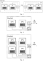
- This on-computation node connectivity might be realized with the technology of the high speed network, a separate on-computation node high speed network or a common memory (as for example in Symmetric-Multiprocessing, SMP, systems). Such an arrangement is illustrated in Fig. 1 .
- Fig. 1 shows an arrangement of multiple computation nodes CN, with each computation node including a plurality of processing elements, PE, each having a respective memory, MEM.
- the computation nodes are connected to each other via a high speed network, HSN, with each computation node including a network interface controller, NIC, for connecting to the high speed network.
- the individual processing elements are connected together and also connect to the network interface controller.
- a processing element has a peak performance, PP, which is the upper limit for the number of (floating point) operations the processing element can execute per second, measured as floating point operations per second or in short "flops" (while floating point operations are referred to, the operations may equally be integer operations).
- the peak performance of a computation node, PPCN is the sum of the peak performances of its processing elements.
- a given application A in general, can realize only a fraction ⁇ A of the peak performance, with 0 ⁇ ⁇ ⁇ 1, ⁇ being called sustained efficiency. The reason for this is that the data transfer rate, i.e, the memory bandwidth (MBW) between the memory of the processing element to its compute registers is finite and thus will decrease the exploitation of the peak performance to ⁇ A for a given application.
- a similar argument can be made for the input/output data transfer rate, i.e. the communication bandwidth (CBW) of a processing element to another processing element off-computation node, potentially further decreasing the exploitation of the peak performance.
- the theoretically possible communication bandwidth is determined by the number of serial lanes available from the processing element to the high speed network (this holds for both CPUs and GPUs). This number is limited by the serializer-deserializer implementation that is constrained on current chip technology.
- NIC network interface controller
- US 2005/0166073 A1 describes the use of a variable operating frequency of system processors in order to maximize a system memory bandwidth.
- US 2011/0167229 A1 describes a computing system comprising multiple computing devices each connected to a storage device, such as a hard drive, as opposed to a memory.
- the aim of the system is to match a data rate of retrieving stored data and a processing speed.
- the suggestion in this document is to use storage units with a higher data transfer rate, i.e. solid state drive in place of or in addition to a hard disk drive, combined with particular low power processors which operate at a lower clock rate.
- US 2015/0095620 A1 describes a technique for estimating the scalability of a workload in a computing system.
- the system has a single multi-core processor.
- the invention provides a method of operating a computing unit comprising a multicore processor and a plurality of graphics processing units, GPUs, each GPU having a nominal peak performance of PPG operations per second, the method comprising operating the GPUs at a fraction 1/ f of their nominal peak performance rate, wherein the computing unit provides a predetermined peak calculation performance of PP operations per second and the computing unit has n times f GPUs such that PP is equal to n times PPG.
- the present invention relates to the fact that a reduction of the clock frequency v of a processing element by a factor f can reduce the energy consumption of the processing element by a factor f or more. This process is called "underclocking".
- a key aspect of the invention is that for processing elements like modern CPUs and GPUs, the compute frequency f can be decreased without, at the same time, decreasing the memory bandwidth of the processing element. As a consequence, the ratio R is increased by a factor f under this modification. It is remarked that it is not possible to increase the operating frequency of the compute cores without adapting the memory speed.
- This invention provides an apparatus that increases the efficiency of parallel processing systems in terms of performance and energy consumption.
- Technical modifications are introduced that reduce the operating frequency of the processing elements and increase the number of processing elements accordingly to achieve the same peak performance of the entire system at increased application performance.
- These modifications affect two system parameters that impact the overall efficiency; the memory to register data bandwidth divided by the peak performance of the processing nodes, and the data bandwidth of the processing nodes into the high-speed network of the parallel system divided by the peak performance of the processing nodes.
- This allows the parallelism of the nodes to be increased with constant or even lower energy consumption of the node. In this manner, the system can be tuned to an optimum of the application performance. The optimum can be selected for any desired measure, e.g.
- the invention presented allows to choose the factor f , which determines the reduction of the processing element frequency and the corresponding increase of the number of processing elements on a computation node, according to selected desired criteria, e.g. the average maximum power for a certain portfolio of applications or the maximum power for a certain application.
- desired criteria e.g. the average maximum power for a certain portfolio of applications or the maximum power for a certain application.
- both modifications can also be applied independently, depending on the influence of system-critical parameters such as energy consumption and investment costs as well as optimal performance, especially with regard to the interaction of architecture and application with regard to scalability.
- This invention can be realized with technology existing today. To give an example, it can be a method to speed up application performances in a booster module within a modular supercomputing system that is aiming at peak exascale performance by 2021 as described in WO 2012/049247 A1 and subsequent applications WO 2018/065 530 A1 and WO 2019/145 354 A1 .
- the goal of the invention is to improve the on-computation node application performance for data-intensive calculations compared to any other architectural design by a factor f , and, in addition, to increase the communication bandwidth in order to keep step with the memory bandwidth for better scaling of many applications with large communication requirements off-computation node.
- a realization is given by a set of computation nodes that use Mellanox BlueField (BF) multicore system on chip technology.
- a BlueField card may comprise multiple graphical processor units, GPUs, a PCIe gen 4 switch and one or more high data rate, HDR, switches. Each BlueField card can be equipped with up to four GPUs.
- the BF cards comprise two Mellanox host channel adaptors, HCAs, each, thus up to two times HDR performance can be achieved off-computation node.
- the AMD Radeon Vega 20 GPU is considered as concrete example for the processing element, expected for general delivery mid of 2018.
- the Vega-20 GPU can be connected to the PCI-e interface on the BF-computation node by 16 PCle gen4 lanes.
- the GPU is expected to be equipped with 32 GigaByte HBM-2 memory, partitioned in four memory banks of 8 GigaByte each. 16 GB of HBM-2 is also a possibility, organized again in four memory banks of 4 GigaByte each.
- the memory rate can be the same for both configurations.
- R 0.1. While this is far off by a factor 10 from the practitioner's rule of 1 byte / flop, it is still one of the best ratios R available.
- the communication bandwidth is capped by 16 PCle gen4 lanes, each capable of 2 Gigabyte per lane and direction.
- the processing element will operate up to one half of the peak performance of the standard configuration.
- the improved computation node the following system parameters are given or are expected:
- the maximum data transfer rate CBW is within 30% of a processing element to processing element communication rate in the computation node.
Landscapes
- Engineering & Computer Science (AREA)
- Theoretical Computer Science (AREA)
- Physics & Mathematics (AREA)
- General Engineering & Computer Science (AREA)
- General Physics & Mathematics (AREA)
- Software Systems (AREA)
- Power Sources (AREA)
- Multi Processors (AREA)
- Advance Control (AREA)
- Image Processing (AREA)
- Image Generation (AREA)
Claims (7)
- Unité informatique pour fonctionnement dans un système informatique parallèle, l'unité informatique comprenant une pluralité d'éléments de traitement et une interface pour connecter l'unité informatique à d'autres composants du système informatique, dans laquelle chaque élément de traitement a un débit de traitement maximum nominal NPR et chaque élément de traitement inclut une unité de mémoire vive respective de manière telle que des données puissent être transférées depuis l'unité de mémoire à un débit de données maximum prédéterminé MBW et l'interface fournit un débit de transfert de données maximum CBW, dans laquelle, afin de fournir une performance de calcul optimale prédéterminée, PP, pour l'unité informatique, obtenable par un nombre n d'éléments de traitement fonctionnant au débit de traitement maximum nominal de manière telle que PP = n x NPR opérations par seconde, l'unité informatique inclut un multiple entier f multiplié par n éléments de traitement, dans laquelle f est supérieur à un et chaque élément de traitement est limité pour fonctionner à un débit de traitement de NPR/f.
- Unité informatique selon la revendication 1, dans laquelle l'unité informatique ayant f multiplié par n éléments de traitement présente une largeur de bande de mémoire de f multiplié par une largeur de bande de mémoire d'une unité informatique ayant n éléments de traitement.
- Unité informatique selon la revendication 1 ou la revendication 2, dans laquelle les éléments de traitement de l'unité informatique sont des unités de traitement graphiques.
- Unité informatique selon une quelconque revendication précédente, dans laquelle les éléments de traitement sont connectés ensemble par une unité d'interface, chaque élément de traitement étant connecté à l'unité d'interface par une pluralité S de voies de données sérielles.
- Unité informatique selon une quelconque revendication précédente, dans laquelle l'unité informatique est une carte d'ordinateur comprenant un processeur multicœur agencé pour commander les éléments de traitement.
- Unité informatique selon une quelconque revendication précédente, dans laquelle le débit de transfert de données maximum CBW est dans les limites de 30 % d'un débit de communication d'un de la pluralité d'éléments de traitement à un autre de la pluralité de éléments de traitement.
- Procédé de fonctionnement d'une unité informatique comprenant un processeur multicœur et une pluralité d'unités de traitement graphiques, GPUs, chaque GPU ayant une performance optimale nominale d'opérations PPG par seconde et une mémoire vive respective, le procédé comprenant le fonctionnement des GPUs à une fraction 1/f de leur débit de performance optimale nominale, dans lequel f est supérieur à un et dans lequel l'unité informatique fournit une performance de calcul optimale prédéterminée de PP opérations par seconde et l'unité informatique a un multiple entier f multiplié par n GPUs de manière telle que PP est égal à n multiplié par PPG.
Priority Applications (1)
| Application Number | Priority Date | Filing Date | Title |
|---|---|---|---|
| HRP20251102TT HRP20251102T1 (hr) | 2018-05-15 | 2019-05-15 | Uređaj i postupak za učinkovito paralelno računanje |
Applications Claiming Priority (2)
| Application Number | Priority Date | Filing Date | Title |
|---|---|---|---|
| EP18172497 | 2018-05-15 | ||
| PCT/EP2019/062483 WO2019219747A1 (fr) | 2018-05-15 | 2019-05-15 | Appareil et procédé de calcul parallèle efficace |
Publications (3)
| Publication Number | Publication Date |
|---|---|
| EP3794448A1 EP3794448A1 (fr) | 2021-03-24 |
| EP3794448C0 EP3794448C0 (fr) | 2025-06-18 |
| EP3794448B1 true EP3794448B1 (fr) | 2025-06-18 |
Family
ID=62217759
Family Applications (1)
| Application Number | Title | Priority Date | Filing Date |
|---|---|---|---|
| EP19723431.3A Active EP3794448B1 (fr) | 2018-05-15 | 2019-05-15 | Appareil et procédé de calcul parallèle efficace |
Country Status (11)
| Country | Link |
|---|---|
| US (1) | US12073259B2 (fr) |
| EP (1) | EP3794448B1 (fr) |
| JP (1) | JP7561033B2 (fr) |
| KR (1) | KR102793011B1 (fr) |
| CN (1) | CN112166414B (fr) |
| CA (1) | CA3097289A1 (fr) |
| ES (1) | ES3040478T3 (fr) |
| HR (1) | HRP20251102T1 (fr) |
| HU (1) | HUE072996T2 (fr) |
| PL (1) | PL3794448T3 (fr) |
| WO (1) | WO2019219747A1 (fr) |
Families Citing this family (1)
| Publication number | Priority date | Publication date | Assignee | Title |
|---|---|---|---|---|
| US20230253294A1 (en) * | 2022-02-09 | 2023-08-10 | Samsung Electronics Co., Ltd. | Computing device and electronic device guaranteeing bandwidth per computational performance |
Family Cites Families (13)
| Publication number | Priority date | Publication date | Assignee | Title |
|---|---|---|---|---|
| JP2002099433A (ja) | 2000-09-22 | 2002-04-05 | Sony Corp | 演算処理システム及び演算処理制御方法、タスク管理システム及びタスク管理方法、並びに記憶媒体 |
| US7321979B2 (en) | 2004-01-22 | 2008-01-22 | International Business Machines Corporation | Method and apparatus to change the operating frequency of system core logic to maximize system memory bandwidth |
| JP4894915B2 (ja) | 2007-03-29 | 2012-03-14 | 富士通株式会社 | 情報処理装置設計方法、情報処理装置設計プログラム |
| US8208395B2 (en) * | 2008-10-31 | 2012-06-26 | Verizon Patent And Licensing Inc. | System and method for measuring interface utilization using policers |
| FR2943158B1 (fr) * | 2009-03-12 | 2011-04-08 | St Wireless Sa | Procede de commande d'un transfert de donnees sur un bus informatique a transmission serie. |
| US20110167229A1 (en) * | 2009-12-16 | 2011-07-07 | The Johns Hopkins University | Balanced data-intensive computing |
| EP2442228A1 (fr) | 2010-10-13 | 2012-04-18 | Thomas Lippert | Agencement de grappe d'ordinateur pour traiter une tâche informatique et son procédé de fonctionnement |
| JP6258335B2 (ja) * | 2012-09-26 | 2018-01-10 | チルドレンズ ナショナル メディカル センターChildren’S National Medical Center | ハーフループクリップを有する吻合クリップツール |
| US9594560B2 (en) * | 2013-09-27 | 2017-03-14 | Intel Corporation | Estimating scalability value for a specific domain of a multicore processor based on active state residency of the domain, stall duration of the domain, memory bandwidth of the domain, and a plurality of coefficients based on a workload to execute on the domain |
| EP3126969A4 (fr) | 2014-04-04 | 2017-04-12 | Microsoft Technology Licensing, LLC | Représentation d'application extensible |
| US10095434B2 (en) | 2015-01-02 | 2018-10-09 | Reservoir Labs, Inc. | Systems and methods for efficient determination of task dependences after loop tiling |
| US20170212581A1 (en) | 2016-01-25 | 2017-07-27 | Qualcomm Incorporated | Systems and methods for providing power efficiency via memory latency control |
| CN107465500B (zh) | 2017-07-20 | 2020-04-03 | 广州慧睿思通信息科技有限公司 | 基于fpga的md5暴力破解系统及方法 |
-
2019
- 2019-05-15 EP EP19723431.3A patent/EP3794448B1/fr active Active
- 2019-05-15 US US17/048,457 patent/US12073259B2/en active Active
- 2019-05-15 WO PCT/EP2019/062483 patent/WO2019219747A1/fr not_active Ceased
- 2019-05-15 ES ES19723431T patent/ES3040478T3/es active Active
- 2019-05-15 KR KR1020207031743A patent/KR102793011B1/ko active Active
- 2019-05-15 HR HRP20251102TT patent/HRP20251102T1/hr unknown
- 2019-05-15 CN CN201980031994.4A patent/CN112166414B/zh active Active
- 2019-05-15 JP JP2020564457A patent/JP7561033B2/ja active Active
- 2019-05-15 CA CA3097289A patent/CA3097289A1/fr active Pending
- 2019-05-15 PL PL19723431.3T patent/PL3794448T3/pl unknown
- 2019-05-15 HU HUE19723431A patent/HUE072996T2/hu unknown
Also Published As
| Publication number | Publication date |
|---|---|
| JP2021523491A (ja) | 2021-09-02 |
| CA3097289A1 (fr) | 2019-11-21 |
| KR20210009311A (ko) | 2021-01-26 |
| HRP20251102T1 (hr) | 2025-11-21 |
| EP3794448A1 (fr) | 2021-03-24 |
| PL3794448T3 (pl) | 2025-10-20 |
| HUE072996T2 (hu) | 2025-12-28 |
| EP3794448C0 (fr) | 2025-06-18 |
| CN112166414B (zh) | 2024-10-15 |
| JP7561033B2 (ja) | 2024-10-03 |
| ES3040478T3 (en) | 2025-10-31 |
| US12073259B2 (en) | 2024-08-27 |
| US20210157656A1 (en) | 2021-05-27 |
| CN112166414A (zh) | 2021-01-01 |
| WO2019219747A1 (fr) | 2019-11-21 |
| KR102793011B1 (ko) | 2025-04-07 |
Similar Documents
| Publication | Publication Date | Title |
|---|---|---|
| US8799623B2 (en) | Hierarchical reconfigurable computer architecture | |
| Pekhimenko et al. | A case for toggle-aware compression for GPU systems | |
| US8713576B2 (en) | Load balancing for parallel tasks | |
| WO2012146471A1 (fr) | Partition dynamique de données pour une utilisation de ressources optimale dans un système de traitement parallèle de données | |
| US20250390220A1 (en) | Access acceleration system for storage device | |
| CN111666253B (zh) | 向具有共享存储器的共享处理元件的系统传递可编程数据 | |
| US20160350074A1 (en) | Highly efficient inexact computing storage device | |
| WO2013048529A1 (fr) | Procédé et appareil pour une technique de compression de dictionnaire à large bande passante à l'aide d'une mise à jour de dictionnaire retardée | |
| EP3794448B1 (fr) | Appareil et procédé de calcul parallèle efficace | |
| Matsuoka et al. | GPU accelerated computing–from hype to mainstream, the rebirth of vector computing | |
| Nukada | Performance optimization of allreduce operation for multi-gpu systems | |
| US10491701B2 (en) | Interconnect method for implementing scale-up servers | |
| Semin et al. | The performance characterization of the RSC PetaStream Module | |
| US12056085B2 (en) | Determining internodal processor interconnections in a data-parallel computing system | |
| Barrett et al. | Reducing the bulk in the bulk synchronous parallel model | |
| EP3963583A1 (fr) | Placement de dimm entrelacé à colonnes multiples et topologie de routage | |
| Schmidtke et al. | Moore’s law redefined for AI/HPC | |
| US20040139297A1 (en) | System and method for scalable interconnection of adaptive processor nodes for clustered computer systems | |
| CN222319458U (zh) | 互联系统和计算机服务器集群 | |
| CN1760835A (zh) | 计算引擎代码空间的扩展 | |
| JP3254552U (ja) | Aiアクセラレータシステムのためのブリッジングネットワークインターフェースデバイスを用いたノード内及びノード間のトランスペアレント通信 | |
| Gunnam et al. | Addition of CXL memory pool to increase LLM training check-pointing frequency | |
| Padyana et al. | Reducing the disk io bandwidth bottleneck through fast floating point compression using accelerators | |
| CN120849343A (zh) | 超宽risc-v长向量处理器 | |
| Spiteri et al. | Accelerators and Cluster Architectures |
Legal Events
| Date | Code | Title | Description |
|---|---|---|---|
| STAA | Information on the status of an ep patent application or granted ep patent |
Free format text: STATUS: UNKNOWN |
|
| STAA | Information on the status of an ep patent application or granted ep patent |
Free format text: STATUS: THE INTERNATIONAL PUBLICATION HAS BEEN MADE |
|
| PUAI | Public reference made under article 153(3) epc to a published international application that has entered the european phase |
Free format text: ORIGINAL CODE: 0009012 |
|
| STAA | Information on the status of an ep patent application or granted ep patent |
Free format text: STATUS: REQUEST FOR EXAMINATION WAS MADE |
|
| 17P | Request for examination filed |
Effective date: 20201208 |
|
| AK | Designated contracting states |
Kind code of ref document: A1 Designated state(s): AL AT BE BG CH CY CZ DE DK EE ES FI FR GB GR HR HU IE IS IT LI LT LU LV MC MK MT NL NO PL PT RO RS SE SI SK SM TR |
|
| AX | Request for extension of the european patent |
Extension state: BA ME |
|
| DAV | Request for validation of the european patent (deleted) | ||
| DAX | Request for extension of the european patent (deleted) | ||
| STAA | Information on the status of an ep patent application or granted ep patent |
Free format text: STATUS: EXAMINATION IS IN PROGRESS |
|
| 17Q | First examination report despatched |
Effective date: 20230313 |
|
| RAP3 | Party data changed (applicant data changed or rights of an application transferred) |
Owner name: PARTEC AG |
|
| GRAP | Despatch of communication of intention to grant a patent |
Free format text: ORIGINAL CODE: EPIDOSNIGR1 |
|
| STAA | Information on the status of an ep patent application or granted ep patent |
Free format text: STATUS: GRANT OF PATENT IS INTENDED |
|
| INTG | Intention to grant announced |
Effective date: 20250120 |
|
| GRAS | Grant fee paid |
Free format text: ORIGINAL CODE: EPIDOSNIGR3 |
|
| GRAA | (expected) grant |
Free format text: ORIGINAL CODE: 0009210 |
|
| STAA | Information on the status of an ep patent application or granted ep patent |
Free format text: STATUS: THE PATENT HAS BEEN GRANTED |
|
| AK | Designated contracting states |
Kind code of ref document: B1 Designated state(s): AL AT BE BG CH CY CZ DE DK EE ES FI FR GB GR HR HU IE IS IT LI LT LU LV MC MK MT NL NO PL PT RO RS SE SI SK SM TR |
|
| REG | Reference to a national code |
Ref country code: GB Ref legal event code: FG4D |
|
| REG | Reference to a national code |
Ref country code: CH Ref legal event code: EP |
|
| REG | Reference to a national code |
Ref country code: DE Ref legal event code: R096 Ref document number: 602019071235 Country of ref document: DE |
|
| REG | Reference to a national code |
Ref country code: CH Ref legal event code: EP |
|
| REG | Reference to a national code |
Ref country code: IE Ref legal event code: FG4D |
|
| U01 | Request for unitary effect filed |
Effective date: 20250702 |
|
| U07 | Unitary effect registered |
Designated state(s): AT BE BG DE DK EE FI FR IT LT LU LV MT NL PT RO SE SI Effective date: 20250708 |
|
| PG25 | Lapsed in a contracting state [announced via postgrant information from national office to epo] |
Ref country code: RS Free format text: LAPSE BECAUSE OF FAILURE TO SUBMIT A TRANSLATION OF THE DESCRIPTION OR TO PAY THE FEE WITHIN THE PRESCRIBED TIME-LIMIT Effective date: 20250918 |
|
| REG | Reference to a national code |
Ref country code: GR Ref legal event code: EP Ref document number: 20250401867 Country of ref document: GR Effective date: 20251009 Ref country code: ES Ref legal event code: FG2A Ref document number: 3040478 Country of ref document: ES Kind code of ref document: T3 Effective date: 20251031 |
|
| REG | Reference to a national code |
Ref country code: SK Ref legal event code: T3 Ref document number: E 47124 Country of ref document: SK |
|
| REG | Reference to a national code |
Ref country code: HR Ref legal event code: T1PR Ref document number: P20251102 Country of ref document: HR |
|
| U1N | Appointed representative for the unitary patent procedure changed after the registration of the unitary effect |
Representative=s name: LESKE, THOMAS; DE |
|
| REG | Reference to a national code |
Ref country code: HU Ref legal event code: AG4A Ref document number: E072996 Country of ref document: HU |
|
| PG25 | Lapsed in a contracting state [announced via postgrant information from national office to epo] |
Ref country code: SM Free format text: LAPSE BECAUSE OF FAILURE TO SUBMIT A TRANSLATION OF THE DESCRIPTION OR TO PAY THE FEE WITHIN THE PRESCRIBED TIME-LIMIT Effective date: 20250618 |
|
| PLBE | No opposition filed within time limit |
Free format text: ORIGINAL CODE: 0009261 |
|
| STAA | Information on the status of an ep patent application or granted ep patent |
Free format text: STATUS: NO OPPOSITION FILED WITHIN TIME LIMIT |
|
| REG | Reference to a national code |
Ref country code: CH Ref legal event code: L10 Free format text: ST27 STATUS EVENT CODE: U-0-0-L10-L00 (AS PROVIDED BY THE NATIONAL OFFICE) Effective date: 20260430 |