EP3794643B1 - Intégration d'un détecteur infrarouge à ondes courtes avec des substrats compatibles cmos - Google Patents
Intégration d'un détecteur infrarouge à ondes courtes avec des substrats compatibles cmos Download PDFInfo
- Publication number
- EP3794643B1 EP3794643B1 EP18726412.2A EP18726412A EP3794643B1 EP 3794643 B1 EP3794643 B1 EP 3794643B1 EP 18726412 A EP18726412 A EP 18726412A EP 3794643 B1 EP3794643 B1 EP 3794643B1
- Authority
- EP
- European Patent Office
- Prior art keywords
- layer
- buffer layer
- slightly doped
- doped buffer
- readout
- Prior art date
- Legal status (The legal status is an assumption and is not a legal conclusion. Google has not performed a legal analysis and makes no representation as to the accuracy of the status listed.)
- Active
Links
Images


Classifications
-
- H—ELECTRICITY
- H04—ELECTRIC COMMUNICATION TECHNIQUE
- H04N—PICTORIAL COMMUNICATION, e.g. TELEVISION
- H04N23/00—Cameras or camera modules comprising electronic image sensors; Control thereof
- H04N23/20—Cameras or camera modules comprising electronic image sensors; Control thereof for generating image signals from infrared radiation only
- H04N23/23—Cameras or camera modules comprising electronic image sensors; Control thereof for generating image signals from infrared radiation only from thermal infrared radiation
-
- H—ELECTRICITY
- H10—SEMICONDUCTOR DEVICES; ELECTRIC SOLID-STATE DEVICES NOT OTHERWISE PROVIDED FOR
- H10F—INORGANIC SEMICONDUCTOR DEVICES SENSITIVE TO INFRARED RADIATION, LIGHT, ELECTROMAGNETIC RADIATION OF SHORTER WAVELENGTH OR CORPUSCULAR RADIATION
- H10F39/00—Integrated devices, or assemblies of multiple devices, comprising at least one element covered by group H10F30/00, e.g. radiation detectors comprising photodiode arrays
- H10F39/011—Manufacture or treatment of image sensors covered by group H10F39/12
- H10F39/018—Manufacture or treatment of image sensors covered by group H10F39/12 of hybrid image sensors
-
- H—ELECTRICITY
- H10—SEMICONDUCTOR DEVICES; ELECTRIC SOLID-STATE DEVICES NOT OTHERWISE PROVIDED FOR
- H10F—INORGANIC SEMICONDUCTOR DEVICES SENSITIVE TO INFRARED RADIATION, LIGHT, ELECTROMAGNETIC RADIATION OF SHORTER WAVELENGTH OR CORPUSCULAR RADIATION
- H10F39/00—Integrated devices, or assemblies of multiple devices, comprising at least one element covered by group H10F30/00, e.g. radiation detectors comprising photodiode arrays
- H10F39/011—Manufacture or treatment of image sensors covered by group H10F39/12
- H10F39/026—Wafer-level processing
-
- H—ELECTRICITY
- H10—SEMICONDUCTOR DEVICES; ELECTRIC SOLID-STATE DEVICES NOT OTHERWISE PROVIDED FOR
- H10F—INORGANIC SEMICONDUCTOR DEVICES SENSITIVE TO INFRARED RADIATION, LIGHT, ELECTROMAGNETIC RADIATION OF SHORTER WAVELENGTH OR CORPUSCULAR RADIATION
- H10F39/00—Integrated devices, or assemblies of multiple devices, comprising at least one element covered by group H10F30/00, e.g. radiation detectors comprising photodiode arrays
- H10F39/10—Integrated devices
- H10F39/12—Image sensors
- H10F39/18—Complementary metal-oxide-semiconductor [CMOS] image sensors; Photodiode array image sensors
- H10F39/184—Infrared image sensors
-
- H—ELECTRICITY
- H10—SEMICONDUCTOR DEVICES; ELECTRIC SOLID-STATE DEVICES NOT OTHERWISE PROVIDED FOR
- H10F—INORGANIC SEMICONDUCTOR DEVICES SENSITIVE TO INFRARED RADIATION, LIGHT, ELECTROMAGNETIC RADIATION OF SHORTER WAVELENGTH OR CORPUSCULAR RADIATION
- H10F39/00—Integrated devices, or assemblies of multiple devices, comprising at least one element covered by group H10F30/00, e.g. radiation detectors comprising photodiode arrays
- H10F39/10—Integrated devices
- H10F39/12—Image sensors
- H10F39/191—Photoconductor image sensors
- H10F39/193—Infrared image sensors
Definitions
- the invention relates to the manufacturing of electromagnetic radiation detector arrays for intensity detection and imaging comprising Complementary Metal Oxide Semiconductor (CMOS) circuits and absorption materials, both sensitive to high temperature. More precisely the invention relates to short-wave infrared (SWIR) detector arrays, to optical systems comprising such arrays and to methods for forming such detector arrays and also to applications thereof.
- CMOS Complementary Metal Oxide Semiconductor
- SWIR short-wave infrared
- Intensity and imaging detectors equally named electromagnetic radiation photodiodes respectively Focal Plane Arrays (FPAs), are designed to convert the optical generation of electron-hole pairs released by impacting photons into electrical signals, further processed by a readout electronics and represented as an image on a computer screen.
- FPAs Focal Plane Arrays
- these detectors also offer spectral resolution, since the energy of each incident photon is proportional to the number of generated electron-hole pairs and thus measurable by pulse height analysis.
- Intensity detector arrays and FPAs employing direct conversion by means of semiconductor absorbers, can currently be implemented in different ways. They can first be achieved by various material depositions. Polycrystalline or amorphous materials may directly be deposited on the readout electronics made from thin film transistors, whereas single crystals - that have better transport properties - could eventually be epitaxial grown on CMOS processed readout wafers, provided specific metallization schemes will allow for high process temperatures. To the current state of knowledge, this option could't be realized so far.
- intensity detector arrays FPAs may be integrated by various bonding processes.
- the absorber is bonded by bump-bonding that allows for the use of any suitable semiconductor material from which large crystals may be grown, such as Si, Ge or GaAs. While with this technique it is a great challenge to push the pixel size below 50 ⁇ m, bump bonding is replaced by fusion bonding, including bonding with a patterned surface such as semiconducting pads surrounded by oxide. Both ways lead to complex structures that prevent a widespread use of the technology.
- the absorber layer and the CMOS layer are monolithically integrated by covalent bonding and subsequent annealing steps. Whereas the pixel size may be reduced by this method, according to our information, an efficient electrically conductive photodiode structure could't be demonstrated till now.
- intensity detector arrays and FPAs may be achieved by different absorber materials that are either application or integration specific, depending on their sensitivity, absorption or manufacturability, among others.
- Si-based detectors can eventually be manufactured without the use of a bonding process as a high-resistivity absorber layer may be epitaxially grown directly on the CMOS Si substrate. The readout electronics is then CMOS processed in this epitaxial layer and the substrate subsequently removed [Mattiazzo, 2013]. While these detectors may be used for ionizing radiation in high-energy physics, detection in the short-wave infrared (SWIR) spectrum is not possible with Si-based absorbers.
- SWIR short-wave infrared
- Wavelengths detection between 1.00 and 1.55 ⁇ m usually requires indium-gallium-arsenide (InGaAs) absorption materials, whereas recent studies have demonstrated that GeSn-type alloys are better candidates with a higher cutoff wavelength and a better sensitivity.
- InGaAs indium-gallium-arsenide
- GeSn-type alloys are better candidates with a higher cutoff wavelength and a better sensitivity.
- the GeSn growth process itself can be performed at low temperature - between 300°C and 330°C - its direct growth on Si is not reliable enough because of lattices mismatch and difference in the dilatation coefficients so that the integration process requires a buffer layer.
- this can only be obtained at high annealing temperatures.
- the invention relates to a method of fabricating an intensity detector array, in particular a short-wave infrared focal plane array (SWIR FPA), comprising a temperature sensitive conversion layer temperature sensitive a CMOS wafer, and a p-n junction in order to allow for an efficient charge collection between both layers.
- SWIR FPA short-wave infrared focal plane array
- the detector array has basically a p-i-n diode structure, further described as an avalanche photodiode (APD) structure including a lightly p-doped i-region.
- APD avalanche photodiode
- the SWIR detector array is realized by a method of fabrication comprising the deposition of a buffer layer onto the CMOS processed wafer and applying energy onto it, comprising the step of using annealing at very short light pulses duration, before providing the conversion layer on top of the buffer layer.
- FPA focal plane array
- the invention is achieved by a method of fabrication of a short-wave infrared detector array comprising a silicon readout wafer having a deposition surface and comprising a CMOS readout layer.
- the short-wave infrared detector array comprises a slightly doped buffer layer situated on said deposition surface and comprises a short-wave infrared light absorption layer, comprising Ge and Sn, situated on said doped buffer layer.
- the method of the invention comprises the steps (A-D) of:
- said absorption layer consists in a Ge 1-x Sn x alloy.
- said absorption layer has a Sn content x between 0.05 ⁇ x ⁇ 0.25.
- said absorption layer consists in a Si x Ge 1-x-z Sn z alloy.
- said absorption layer has a Si content x between 0 ⁇ x ⁇ 0.2.
- said absorption layer has a Sn content z between 0.05 ⁇ z ⁇ 0.15.
- said absorption layer comprises an i-type Ge 1-x Sn x layer, in contact with said slightly doped buffer layer.
- said i-type Ge 1-x Sn x layer has a thickness between 250nm and 5 ⁇ m, preferably between 250 ⁇ m and 3 ⁇ m.
- said absorption layer comprises, between said slightly doped buffer layer and said i-type Ge 1-x Sn x layer, a p+-type doped Ge 1-x Sn x layer having a doping concentration between 10 19 to 5 ⁇ 10 20 cm -3 .
- said absorption layer comprises an i-type Si x Ge 1-x-z Sn z layer, in contact with said slightly doped buffer layer.
- the thickness of said absorption layer in all the embodiments of the invention is between 2 nm and 5 ⁇ m.
- the absorption layer is realized by an epitaxial lift-off process.
- said slightly doped buffer layer is a p-type doped Ge layer having a doping concentration between 10 14 to 10 15 cm -3 .
- said slightly doped buffer layer is realized by a technology including wafer-bonding and a layer splitting process.
- said slightly doped buffer layer is realized by an epitaxial lift-off transfer process.
- said slightly buffer layer is a p-type doped Ge 1-x Sn x layer having a doping concentration between 10 14 to 10 15 cm -3 .
- said p-type doped Ge 1-x Sn x buffer layer is realized by a technology including wafer-bonding and a layer splitting process.
- said buffer layer is realized by a technology including wafer-bonding and an etch back and/or polishing process.
- said slightly doped buffer layer is realized by an epitaxial lift-off transfer process.
- the thickness of said slightly doped buffer layer in all the embodiments of the invention is between 5 nm and 3 ⁇ m.
- said slightly doped buffer layer is etched after step B or after step C so as to provide an etched area of said slightly doped buffer layer.
- said slightly doped buffer layer is at least partially covered after step B or after step C so as to provide a selectively covered area of said slightly doped buffer layer.
- said etched area is covered by materials selected from: SiO x , SiN, Al 2 O 3 .
- said selectively covered area is covered by materials selected from: SiO x , SiN, Al 2 O 3 .
- the annealing temperature of said interface layer during the annealing process step C is higher than 650°C and lower than 750°C.
- said light source provides light having a wavelength that is comprised between 300 nm and 900 nm.
- the light is provided by a pulsed light source providing light pulses having a pulse duration of said light pulses lower than 1 ms, preferably lower than 100 ns.
- the light source comprises at least one laser.
- the light source comprises at least one pulsed lamp.
- Fig. 1 illustrates a SWIR detector array 1 of prior art.
- a detector array comprises typically a microlens array (A) and an absorber sheet typically made of InGaAs (B), as well as a readout circuit realized on a separate layer or wafer.
- the stack comprising the optical layer (A) and the absorber layer (B) is electrically and mechanically connected to the CMOS layer (C) by an array of bumps (D).
- the device of the invention provides a highly efficient monolithic SWIR detector array 1 comprising a simplified 3D integrated structure having a small thickness, a reduced weight and lower power requirements.
- the SWIR detector array 1 of the invention is also called a focal plane array (FPA) hereafter.
- FPA focal plane array
- the device of the invention allows to provide very sensitive and large area monolithic FPAs able to cover efficiently the whole SWIR spectrum at room-temperature or eventually Peltier-cooled operation.
- Said SWIR spectrum is defined by a wavelengths range between 1.0 ⁇ m and 3.0 ⁇ m.
- the SWIR detector array 1 of the invention illustrated in Fig. 3 , comprises at least:
- the SWIR detector array 1 of the invention may be configured to be suited for intensity measurements or as an imaging array in which case the detector array is called a Focal Plane Array as it is intended to be placed in the focal plane of an optical system.
- the SWIR detector array 1 comprises also an electrical contact layer 50 and a back contact configured to apply an electrical potential across the layers of the detector array 1.
- the electrical contact layer 50 may be a metallic layer, a transparent conducting layer or may be a doped layer such as a highly p or n-doped layer.
- said readout wafer 20 is a p-doped or n-doped wafer, but not necessarily so.
- the readout wafer of the detector 1 of the invention may be configured in different ways but comprises always at least one electrical charge collecting area.
- the readout wafer comprises an array of electrical charge collecting structures.
- the electrical charge collecting structures are preferably doped regions.
- the array of electrical charge collecting structures may be a 2D array, for example an array comprising 50 x 50 electrical charge collecting areas.
- the array of charge collectors array may be a 1D array, comprising at least two charge collecting areas, which can be particularly useful in intensity detection applications comprising waveguides as described further.
- the, 1D or 2D SWIR detector array 1 may be made of an assembly of SWIR detectors 1 of the invention, comprising each a low number of electrical charge collecting areas, for example 10 electrical charge collecting areas per detector array 1.
- the detector array 1 may comprise widely spaced charge collecting areas.
- the detector array 1 is a FPA comprising densely packed charge collecting areas, as illustrated in Fig. 5 illustrating a single pixel of a FPA.
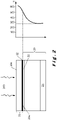
- Fig. 4 illustrates the electrical field across an embodiment of the SWIR detector array 1 in operation.
- the electrical potential drop across the detector array 1 produces an electrical field E, illustrated in the graph of Fig. 4.
- Fig. 4 illustrates also an avalanche region (AV) provided by an electrical field E applied across the detector array 1.
- AV avalanche region
- the readout electronics is preferably processed in an epitaxial Si layer with a thickness of about 10 - 30 ⁇ m and a resistivity above about 500 Qcm or preferably about 1 - 2 k ⁇ cm or more preferably 2 - 5 k ⁇ 2cm or even above 5 k ⁇ cm, for example 5 - 50 k ⁇ cm, the resistivity being due to a low doping level in between about 10 11 to 10 13 cm -3 of a first conduction type (for example n-conduction induced by n-doping).
- silicon-on-insulator (SOI) wafers may be used for the CMOS processing of the readout electronics.
- SOI silicon-on-insulator
- a silicon layer 20 may comprise n+ charge collectors 24.
- said absorption layer 40 is a lightly p-doped layer. In operation, each photon incident on the absorption layer 40 creates an electron-hole pair in the absorber 40. The hole is collected at the incident light side and the electron, created by the absorption of a photon, drifts to the avalanche region AV ( Fig.
- the SWIR detector array 1 such as a FPA of the invention provides single-photon detection. It is therefore suitable for energy discrimination, whereby the energy of photons incident on the absorber can be measured by employing the pulse height analysis of the electrical pulses processed by the readout electronics.
- said buffer layer 30 consists of a slightly doped Ge layer and is preferably a p-type doped Ge layer having a doping concentration between 10 14 to 10 15 cm -3 .
- said slightly doped buffer layer 30 is made of Ge 1-x Sn x and has a Sn content x between 0.00 ⁇ x ⁇ 0.03, and is preferably a p-type doped Ge 1-x Sn x layer having a doping concentration between 10 14 to 10 15 cm -3 .
- said slightly doped buffer layer 30 may be advantageously be realized by an epitaxial lift-off transfer process.
- said buffer layer (30 is realized by a technology including wafer-bonding and an etch back and/or a polishing process.
- said absorption layer 40 consists in a Ge 1-x Sn x alloy.
- Said absorption layer 40 has preferably a Sn content x between 0.05 ⁇ x ⁇ 0.25.
- said absorption layer 40 consists in a Si x Ge 1-x-z Sn z alloy and has preferably a Si content x between 0 ⁇ x ⁇ 0.2.
- the absorption layer 40 consisting in a Si x Ge 1-x-z Sn z alloy said absorption layer 40 has a Sn content z between 0.05 ⁇ z ⁇ 0.15.
- said absorption layer 40 comprises an i-type Ge 1-x Sn x layer 42 being in contact with said slightly doped buffer layer 30. This layer can absorb up to 100% of the incident light with a photon wavelength greater than 1.4 ⁇ m, depending on the thickness.
- Said i-type Ge 1-x Sn x layer may have a thickness between 250 nm and 5 ⁇ m, preferably between 250 nm and 3 ⁇ m.
- said absorption layer 40 comprises, between said slightly doped buffer layer 30 and said i-type Ge 1-x Sn x layer 42, a p + -type doped Ge 1-x Sn x layer 44 having a doping concentration between 10 19 to 5 ⁇ 10 20 cm -3 .
- said absorption layer 40 comprises an i-type Si x Ge 1-x-z Sn z layer, in contact with said slightly doped buffer layer 30.
- said absorption layer 40 comprises, between said slightly doped buffer layer 30 and said i-type Si x Ge 1-x-z Sn z layer, a p+-type doped Ge 1-x Sn x layer having a doping concentration between 10 19 to 5x1020 cm -3 .
- the thickness of the absorption layer 40 is between 2 nm and 5 ⁇ m. In a variant, the thickness of the absorption layer 40 is between 1nm and 1000 ⁇ m.
- an etched area 34 may be provided in the buffer layer 30.
- This etched area 34 extends across the whole thickness of the buffer layer 30 and may serve to deposit other materials, different to the buffer material, directly on said deposition surface 20a. These added other materials my serve to avoid the growth of absorption alloys such as Ge 1-x Sn x and Si x Ge 1-x-z Sn z over predetermined areas.
- said etched area 34 may be covered by materials selected from: SiO x wherein 1.9 ⁇ x ⁇ 2.0, SiN, HfO, Al 2 O 3 . Said coverage is not limited to these materials.
- a portion of the buffer layer 30 may also comprise a selectively covered area that is covered by materials selected from: SiO x wherein 1.9 ⁇ x ⁇ 2.0, SiN, HfO, Al 2 O 3 . These added other materials my serve to avoid the growth of absorption alloys such as Ge 1-x Sn x and Si x Ge 1-x-z Sn z on the whole extension of the buffer layer.
- At least a portion of said etched area 34 and a portion of said buffer layer 30 may be covered by materials selected from: SiO x wherein 1.9 ⁇ x ⁇ 2.0, SiN, HfO, Al 2 O 3 .
- said etched area 34 and a portion of said buffer layer 30 are covered by different materials.
- an optical layer having optical focusing properties may be arranged between said absorption layer 40 and said buffer layer.
- at least one side of said absorption layer 30 may be corrugated and have for example the shape of an array of microlenses so as to provide a focused light beam on a focal plane coincident with said interfacial layer 32.
- the interface layer 32 will have the same structured or corrugated shape as the structured or corrugated surface of said absorption layer 30.
- an antireflection coating is added in order to maximize the amount of light coupled into the device/absorbing layer.
- composition and thickness of any of the layers of the detector 1 may be configured so as to shape a predetermined electrical field profile across the avalanche region (AV) of the detector 1. Shaping electrical field profiles is well known in the art and is not further commented here.
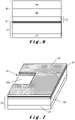
- FIG. 5 An exemplary execution of a small part of the cross-section of the thinned CMOS processed readout wafer 20 of a SWIR detector array 1 comprises a p-n junction 22 is now described and illustrated in Fig. 5 .
- the width of the section illustrated in figure 5 defined in the plane of the readout wafer 21, corresponds to slightly more than a single pixel size of the detector array 1, and may range for example from 5 -20 ⁇ m,20 - 50 ⁇ m,50 -100 ⁇ m, depending on the CMOS process used.
- n-wells 25 serve as charge collectors, collecting electrons coming from electron-hole pairs which are generated by incident photons and separated in the electric field of the p-n junction formed by a preferably lightly n-doped Si CMOS processes readout wafer 20 and a lightly p-doped layer.
- the distance between adjacent n-wells 25 defines the pixel size of the detector array.
- n-MOS transistors of the pixel electronics of the readout are situated in p-wells 26 and n-wells 23, respectively.
- a deep p-well 24 arranged on said p-wells 26 and n-wells 23, has the purpose of avoiding electron collection by n-wells 23 in addition to charge collecting by n-well 25.
- part of the pixel electronics may be located in n-well 25.
- the p-n junction 22 is inside the readout wafer, preferably at the interface between a lightly p-doped layer and a lightly n-doped main part of SOI wafer 20.
- the lightly n-doped main part of SOI wafer 20 comprises preferably a thin, lightly p-doped Si layer with a highly resistive n-doped layer on top, hosting the CMOS processed readout.
- the lightly p-doped layer may have a thickness of about 1- 2 ⁇ m, 2 - 5 ⁇ m or even in the range from 5 - 50 ⁇ m or 50 - 100 ⁇ m. Substrate and buried oxide of the SOI wafer are thereby removed prior to further processing of the device.
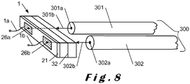
- the detector array 1 may comprise electrical connections such as electrical wires 1a, 1b, connected to said charge collecting areas as illustrated in Fig.8 .
- a SWIR detector array 1 may be configured as a linear array of SWIR detectors having said charge collecting arrays 26a, 26b arranged linearly. This can be useful for example to detect the intensity of light provided by the output surfaces of a linear array 300 of fibers.
- a SWIR detector array 1 may be configured so that each charge collecting area 26 faces the output surface of a fiber of a fiber bundle 300, as illustrated in Fig. 8 .
- the fiber bundle 300 may be arranged according to a circular arrangement or according to another arrangement such as a square, hexagonal, or rectangular arrangement.
- the invention is also realized by a SWIR detection system 3 comprising an array 300 of waveguides 301-305 and a SWIR detector array 1 as described, and of which a portion only is illustrated in Fig.10 .
- the waveguides may be fiber optics or planar waveguides.
- the waveguides may be mono-mode waveguides or multimode waveguides.
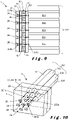
- said optical fibers are arranged in specific 2 dimensions, such as a hexagonal arrangement of fiber optics as shown in Fig.10 , or in a linear array as illustrated in Fig. 8 .
- Other geometrical configurations of the waveguides are also possible.
- a stack of flat substrates comprising each at least one waveguide may be arranged in said SWIR detection system 3.
- the cores 301a-305a of the waveguides 301-305 are facing a charge collector as illustrated in Fig. 8-10 .
- Realizing a SWIR detection system 3 wherein the charge collectors have the same geometrical distribution than the one of the waveguide array 300, as illustrated in Figs. 9 and 10 is particularly interesting to provide an SWIR imaging system wherein an image is transferred from one end of a waveguide array 300 , such as a fiber bundle, to another end of the array. Butt-coupling a bundle of waveguides such as a fiber bundle is known to the skilled person and is not further described herein.
- optical fibers may be arranged at a predetermined distance relative to the entry face of the detector, which may be for example the contact layer 50.
- the gap layer 60 separating the entry face of the detector 1 and the outcoupling surfaces of the waveguides may be air or may be a SWIR transparent material, such as a glue layer or any other material transparent in the SWIR wavelength range.
- a gap layer may also comprise focusing lenses, such as an array of microlenses.
- the skilled person knows how to incouple light, in various ways, into a bundle of waveguides or fibers, therefore the incoupling portion of the imaging system 3, situated opposite to the outcoupling surfaces 301a-305a is not illustrated in the figures.
- the number of waveguides may be more than 100, more than 1000 or more than 10000.
- the distance between the waveguides or fibers may vary according to the application.
- the optical fibers are arranged in contact and according to a hexagonal distribution such as illustrated in Fig.10 which illustrates only 7 fibers of a closed packed optical fiber bundle.
- the detector array 1 of a SWIR detection system 3, particularly an imaging SWIR detection system 3 may comprise covered portions 36 on said buffer layer 30.
- said covered portions 36 may be realized only on etched areas 34 of the buffer layer 30 and/or may partially cover a portion of the buffer layer 30.
- Such covered portions 36 may be implemented in configurations such as the one illustrated in Fig.9 so as to reduce light cross coupling effects, which may be produced by light emitted by a waveguide and transmitted to a charge collecting area that does not face that waveguide.
- a waveguide array 300 such as a fiber bundle
- SWIR detector array By monolithically integrating a waveguide array 300, such as a fiber bundle, to a SWIR detector array, cheap and robust SWIR flexible imaging systems may be provided.
- the invention is also achieved by a method of fabrication of a short-wave infrared detector array 1 comprising a silicon readout wafer 20 having a deposition surface 20a and comprising a CMOS readout layer.
- the short-wave infrared detector array 1 comprises a slightly doped buffer layer 30 situated on said deposition surface 20a and comprises a short-wave infrared light absorption layer 40, comprising Ge and Sn, situated on said doped buffer layer 30.
- the deposition of a buffer layer 30 between the Si CMOS processed readout wafer and the absorption layer is an essential step to overcome the differences of lattices and dilatation coefficients between Si and materials such as alloys of the type Ge 1-x Sn x or Si x Ge 1-x-z Sn z .
- the method of the invention comprises the steps (A-D) of:
- said absorption layer 40 consists in a Ge 1-x Sn x alloy.
- said absorption layer 40 has a Sn content x between 0.05 ⁇ x ⁇ 0.25.
- said absorption layer 40 consists in a Si x Ge 1-x-z Sn z alloy.
- said absorption layer 40 has a Si content x between 0 ⁇ x ⁇ 0.2.
- said absorption layer 40 has a Sn content z between 0.05 ⁇ z ⁇ 0.15.
- said absorption layer 40 comprises an i-type Ge 1-x Sn x layer, in contact with said slightly doped buffer layer 30.
- said i-type Ge 1-x Sn x layer has a thickness between 250 nm and 5 ⁇ m,preferably between 250 nm and 3 ⁇ m.
- said absorption layer comprises, between said slightly doped buffer layer and said i-type Ge 1-x Sn x layer, a p + -type doped Ge 1-x Sn x layer having a doping concentration between 10 19 to 5 ⁇ 10 20 cm -3 .
- said absorption layer comprises an i-type Si x Ge 1-x-z Sn z layer, in contact with said slightly doped buffer layer 30.
- the thickness of said absorption layer 40 in all the embodiments of the invention is between 2 nm and 5 ⁇ m.
- the absorption layer 40 is realized by an epitaxial lift-off process.
- a thin film of germanium is realized on a layer of a material that can be selectively etched, for example GaAs or AIGaAs or a combination of both. This layer is then bonded on a CMOS substrate. Subsequently the GaAs or AIGaAs (or combination) is selectively etched so that the Ge is freed from the original substrate and transferred to the CMOS substrate.
- said absorption layer may be realized by successively deposited layers of Ge and Sn. These successively deposited layers may have different thicknesses.
- said slightly doped buffer layer 30 is a p-type doped Ge layer having a doping concentration between 10 14 to 10 15 cm -3 .
- said slightly doped buffer layer 30 is realized by a technology including wafer-bonding and a layer splitting process.
- a typical example of such a process is the know Smartcut process which is a Trademark as described in: http://www.soitec.com/fr/produits/smart-cut.
- Ge deposited on a substrate is implanted with hydrogen ions (H + ) with a dose comprised between 5 x 10 16 and 5 x 10 17 cm -2 and an energy comprised between 1keV and 100keV. It is then bonded to the CMOS substrate and flash annealed in order to separate the Ge layer from its substrate.
- the final structure comprises the CMOS substrate comprising a thin Ge layer that has split off from the original implanted Ge substrate.
- the implantation comprises a co-implantation with He + up to 50% of the total implanted dose of Ge and He.
- said slightly doped buffer layer 30 is realized by an epitaxial lift-off transfer process similar to the epitaxial lift-off transfer process of said absorption process as described above.
- said slightly buffer layer 30 is a p-type doped Ge 1-x Sn x layer having a doping concentration between 10 14 to 10 15 cm -3 .
- said p-type doped Ge 1-x Sn x buffer layer is realized also by said technology including wafer-bonding and a layer splitting process. Similar as described before, a typical example of such a process is the known Smartcut process (Trademark of Soitec).
- said slightly doped buffer layer is realized by an epitaxial lift-off transfer process.
- a thin film of Ge 1-x Sn x is realized on a substrate made of a material that can be selectively etched, for example GaAs or AIGaAs or a combination of both.
- the substrate is then bonded on the CMOS substrate.
- the GaAs or AIGaAs (or combination) is selectively etched so that the Ge 1-x Sn x layer is freed from the original substrate and transferred to the CMOS substrate.
- the thickness of said slightly doped buffer layer in all the embodiments of the invention is between 5 nm and 3 ⁇ m.
- said slightly doped buffer layer is etched after step B or after step C so as to provide an etched area of said slightly doped buffer layer.
- said slightly doped buffer layer is at least partially covered after step B or after step C so as to provide a selectively covered area of said slightly doped buffer layer.
- said etched area 34 is preferably covered by materials selected from: SiO x wherein 1.9 ⁇ x ⁇ 2.0, SiN, HfO, Al 2 O 3 . Said etched area 34 may also be covered by other materials that avoid the growth of a SWIR absorbing layer on the covered area.
- said selectively covered area is covered by materials selected from: SiO x , SiN, Al 2 O 3 .
- the annealing temperature of said interface layer during the annealing process step C is higher than 650°C and lower than 750°C.
- said light source provides light having a wavelength that is comprised between 300 nm and 900 nm.
- the light is provided by a pulsed light source providing light pulses having a pulse duration of said light pulses lower than 1 ms, preferably lower than 100 ns.
- the light source comprises at least one laser.
- the light source comprises at least one pulsed lamp.
- the invention is also achieved by a detector array realized according to the above described fabrication method.
- the deposition process may be achieved by different ways that determine the performance of the detector as well as the industrial scalability of its manufacturing.
- the optical layer 500 comprises an array of refractive microlens, or an array of diffractive microlenses, or an array of aspheric shaped microlenses, or an array of microprisms or an array of plasmonic planar metalenses allowing for multi/hyper-spectral imaging and analysis.
- the SWIR detector array such as a FPA
- FPA field-specific integrated circuit
- the SWIR detector array may be used in various types of applications such as ground, airborne and space technology for intelligence, surveillance, military, security or encryption systems. It may also be used for spectroscopy, machine vision or non-invasive clinical investigations such as optical coherence tomography. More precisely, the SWIR detector array can be integrated into and used in methods of the following fields of applications as described below.
- System-level benefits of large FPAs are related to providing a large instantaneous field of view and a fully electronic selection by reading out a region of interest (FOV).
- Large FPAs allow monitoring of large areas and enable key applications, such as high-resolution, wide-area airborne persistent surveillance.
- the detector larger format with smaller pixel size helps to solve the unmanned - aerial or terrestrial - vehicle (UV) automated "sense and avoid” problem.
- UV unmanned - aerial or terrestrial - vehicle
- the mechanical scanning needed in single-detector systems can be avoided and because a photon-counting FPA has the ability to digitally time stamp individual photon arrivals it is an enabler for highly sensitive light detection and ranging (“LIDAR”) imaging systems.
- LIDAR highly sensitive light detection and ranging
- each single-photon avalanche diode measures photon arrival time, and therefore depth to the corresponding point in the scene whereas the image is built up by combining multiple frames.
- Multi/ hyper-spectral LIDAR imaging can thus provide a powerful tool for mapping, archaeology, earth science, glaciology, agricultural assessment and disaster response.
Landscapes
- Engineering & Computer Science (AREA)
- Multimedia (AREA)
- Signal Processing (AREA)
- Health & Medical Sciences (AREA)
- Toxicology (AREA)
- Solid State Image Pick-Up Elements (AREA)
- Light Receiving Elements (AREA)
Claims (14)
- Procédé de fabrication d'un réseau de détecteurs infrarouges à ondes courtes (1) comprenant une tranche de lecture à base de silicium (20), présentant une surface de dépôt (20a), comprenant une couche de CMOS de lecture (21) comprenant au moins deux structures de collecte de charge, ledit réseau de détecteurs infrarouges à ondes courtes (1) comprenant une couche tampon légèrement dopée (30) située sur ladite surface de dépôt (20a) et une couche d'absorption de lumière infrarouge à ondes courtes (40), comprenant du Ge et du Sn, située sur ladite couche tampon dopée (30),
le procédé comprenant les étapes (A-D) de :A. fabrication d'une tranche de lecture (20) présentant une surface de dépôt (20a) et comprenant une couche de CMOS de lecture à base de silicium (21) et une jonction p-n (22) ;B. disposition, sur ladite surface de dépôt (20a), d'une couche tampon légèrement dopée (30) comprenant au moins du Ge et présentant une couche d'interface (32) en contact avec ladite surface de dépôt (20a), ladite couche tampon légèrement dopée (30) comprenant sur son côté opposé à ladite tranche de lecture (20) une surface de couche tampon exempte d'oxyde (30a) ;C. envoi d'impulsions lumineuses (200), fournies par une source de lumière située sur le côté de ladite couche tampon légèrement dopée (30) opposé à ladite tranche de lecture (20), de façon à cristalliser ladite couche d'interface (32) par l'effet de recuit de la chaleur fournie par l'absorption desdites impulsions lumineuses (200) par ladite couche d'interface (32) et de telle sorte que la température de la couche de CMOS de lecture (21) reste inférieure à 350 °C pendant le procédé de recuit ;D. dépôt, sur ladite couche tampon légèrement dopée (30), à des températures inférieures à 350 °C, de ladite couche d'absorption (40). - Procédé selon la revendication 1, ladite couche d'absorption (40) comprenant une couche de Ge1-xSnx de type i, en contact avec ladite couche tampon légèrement dopée (30).
- Procédé selon la revendication 2, ladite couche de Ge1-xSnx de type i présentant une épaisseur située entre 250 nm et 5 µm, préférablement entre 250 nm et 3 µm.
- Procédé selon les revendications 2 ou 3, ladite couche d'absorption (40) comprenant, entre ladite couche tampon légèrement dopée (30) et ladite couche de Ge1-xSnx de type i, une couche de Ge1-xSnx dopée de type p+ présentant une concentration de dopage entre 1019 et 5×1020 cm-3.
- Procédé selon l'une quelconque des revendications 1 à 4, la couche d'absorption (40) étant réalisée par un procédé de retrait épitaxial.
- Procédé selon l'une quelconque des revendications 1 à 5, ladite couche tampon légèrement dopée (30) étant une couche de Ge dopée de type p présentant une concentration de dopage entre 1014 et 1015 cm-3.
- Procédé selon l'une quelconque des revendications 1 à 6, ladite couche tampon légèrement dopée (30) étant réalisée par une technologie comprenant une liaison de tranche et un procédé de séparation de couche.
- Procédé selon l'une quelconque des revendications 1 à 6, ladite couche tampon légèrement dopée (30) étant réalisée par une technologie comprenant une liaison de tranche et un procédé de gravure en retrait et/ou de polissage.
- Procédé selon l'une quelconque des revendications 1 à 6, ladite couche tampon légèrement dopée (30) étant réalisée par un procédé de transfert par retrait épitaxial.
- Procédé selon l'une quelconque des revendications 1 à 9, ladite couche tampon légèrement dopée (30) étant une couche de Ge1-xSnx dopée de type p présentant une concentration de dopage entre 1014 et 1015 cm-3.
- Procédé selon la revendication 10, ladite couche tampon de Ge1-xSnx dopée de type p (30) étant réalisée par une technologie comprenant une liaison de tranche et un procédé de séparation de couche.
- Procédé selon l'une quelconque des revendications 1 à 11, l'épaisseur de ladite couche tampon légèrement dopée (30) étant située entre 5 nm et 3 µm.
- Procédé selon l'une quelconque des revendications 1 à 12, ladite couche tampon légèrement dopée (30) étant gravée après l' étape B ou après l' étape C de façon à réaliser une zone gravée (34) de la couche tampon (30).
- Procédé selon l'une quelconque des revendications 1 à 13, la lumière étant fournie par une source de lumière pulsée fournissant des impulsions lumineuses (200) présentant une durée d'impulsion desdites impulsions lumineuses (200) inférieure à 1 ms, préférablement inférieure à 100 ns.
Applications Claiming Priority (1)
| Application Number | Priority Date | Filing Date | Title |
|---|---|---|---|
| PCT/EP2018/062763 WO2019219189A1 (fr) | 2018-05-16 | 2018-05-16 | Détecteur infrarouge à ondes courtes et son intégration avec des substrats compatibles cmos |
Publications (2)
| Publication Number | Publication Date |
|---|---|
| EP3794643A1 EP3794643A1 (fr) | 2021-03-24 |
| EP3794643B1 true EP3794643B1 (fr) | 2022-06-22 |
Family
ID=62222645
Family Applications (1)
| Application Number | Title | Priority Date | Filing Date |
|---|---|---|---|
| EP18726412.2A Active EP3794643B1 (fr) | 2018-05-16 | 2018-05-16 | Intégration d'un détecteur infrarouge à ondes courtes avec des substrats compatibles cmos |
Country Status (3)
| Country | Link |
|---|---|
| US (1) | US20210210544A1 (fr) |
| EP (1) | EP3794643B1 (fr) |
| WO (1) | WO2019219189A1 (fr) |
Families Citing this family (4)
| Publication number | Priority date | Publication date | Assignee | Title |
|---|---|---|---|---|
| EP3738147B1 (fr) * | 2018-01-12 | 2021-11-24 | IRIS Industries SA | Détecteur infrarouge à ondes courtes et son intégration avec des substrats compatibles cmos |
| CN111708044B (zh) * | 2020-06-20 | 2021-07-06 | 桂林理工大学 | 机载超连续激光50个波段高光谱雷达系统 |
| US12446340B2 (en) * | 2021-08-05 | 2025-10-14 | Sri International | Sensor with upconversion layer |
| CN115128627B (zh) * | 2022-06-01 | 2025-06-17 | 北京空间机电研究所 | 天基红外探测空天高速目标脉冲视觉载荷处理系统及方法 |
Family Cites Families (5)
| Publication number | Priority date | Publication date | Assignee | Title |
|---|---|---|---|---|
| US7651880B2 (en) * | 2006-11-04 | 2010-01-26 | Sharp Laboratories Of America, Inc. | Ge short wavelength infrared imager |
| US20090020700A1 (en) * | 2007-07-17 | 2009-01-22 | Locheed Martin Corporation | Method and device for generating an electrical signal in response to light |
| CN102280456B (zh) * | 2011-05-11 | 2013-06-26 | 北京大学 | 一种红外焦平面阵列探测器集成结构及制作方法 |
| US9472588B1 (en) * | 2015-06-19 | 2016-10-18 | International Business Machines Corporation | Monolithic visible-infrared focal plane array on silicon |
| CN109964315A (zh) * | 2016-08-31 | 2019-07-02 | G射线瑞士公司 | 包括跨越键合界面的电荷输送的电磁辐射检测器 |
-
2018
- 2018-05-16 US US17/055,269 patent/US20210210544A1/en not_active Abandoned
- 2018-05-16 EP EP18726412.2A patent/EP3794643B1/fr active Active
- 2018-05-16 WO PCT/EP2018/062763 patent/WO2019219189A1/fr not_active Ceased
Also Published As
| Publication number | Publication date |
|---|---|
| EP3794643A1 (fr) | 2021-03-24 |
| WO2019219189A1 (fr) | 2019-11-21 |
| US20210210544A1 (en) | 2021-07-08 |
Similar Documents
| Publication | Publication Date | Title |
|---|---|---|
| US10854656B2 (en) | Short-wave infrared detector array and method for the manufacturing thereof | |
| CN114754864B (zh) | 宽频谱光学传感器 | |
| EP2403011B1 (fr) | Elément de détection de lumière à semi-conducteur | |
| EP2756523B1 (fr) | Dispositif de photodétecteur infrarouge à barrière éclairé par la face avant et procédés de fabrication de ce dernier | |
| EP3738147B1 (fr) | Détecteur infrarouge à ondes courtes et son intégration avec des substrats compatibles cmos | |
| JP5829224B2 (ja) | Mosイメージセンサ | |
| EP3794643B1 (fr) | Intégration d'un détecteur infrarouge à ondes courtes avec des substrats compatibles cmos | |
| US20130043372A1 (en) | Multi-Band Position Sensitive Imaging Arrays | |
| US20190214428A1 (en) | Germanium-modified, back-side illuminated optical sensor | |
| US7795639B2 (en) | Avalanche photodiode | |
| KR102153209B1 (ko) | 직접 판독 픽셀 정렬 | |
| KR102467958B1 (ko) | 단파 적외선 스펙트럼 체계에 대한 게르마늄 기반 초점 평면 배열 | |
| US11133349B2 (en) | Short-wave infrared detector array and fabrication methods thereof | |
| Sood et al. | Development of low dark current SiGe-detector arrays for visible-NIR Imaging Sensor | |
| Sood et al. | Characterization of SiGe-detector arrays for visible-NIR imaging sensor applications | |
| Rogalski | Photon detectors | |
| Sood et al. | Development of SiGe arrays for visible-near IR applications | |
| TWI917117B (zh) | 用以製造影像感測陣列之方法 | |
| KR20240136073A (ko) | 이미지 센서 및 그 제조 방법 |
Legal Events
| Date | Code | Title | Description |
|---|---|---|---|
| STAA | Information on the status of an ep patent application or granted ep patent |
Free format text: STATUS: UNKNOWN |
|
| STAA | Information on the status of an ep patent application or granted ep patent |
Free format text: STATUS: THE INTERNATIONAL PUBLICATION HAS BEEN MADE |
|
| PUAI | Public reference made under article 153(3) epc to a published international application that has entered the european phase |
Free format text: ORIGINAL CODE: 0009012 |
|
| STAA | Information on the status of an ep patent application or granted ep patent |
Free format text: STATUS: REQUEST FOR EXAMINATION WAS MADE |
|
| 17P | Request for examination filed |
Effective date: 20201106 |
|
| AK | Designated contracting states |
Kind code of ref document: A1 Designated state(s): AL AT BE BG CH CY CZ DE DK EE ES FI FR GB GR HR HU IE IS IT LI LT LU LV MC MK MT NL NO PL PT RO RS SE SI SK SM TR |
|
| AX | Request for extension of the european patent |
Extension state: BA ME |
|
| RIN1 | Information on inventor provided before grant (corrected) |
Inventor name: FONTCUBERTA MORRAL, ANNA Inventor name: CHUNG, MINTAE |
|
| DAV | Request for validation of the european patent (deleted) | ||
| DAX | Request for extension of the european patent (deleted) | ||
| GRAP | Despatch of communication of intention to grant a patent |
Free format text: ORIGINAL CODE: EPIDOSNIGR1 |
|
| STAA | Information on the status of an ep patent application or granted ep patent |
Free format text: STATUS: GRANT OF PATENT IS INTENDED |
|
| INTG | Intention to grant announced |
Effective date: 20220211 |
|
| GRAS | Grant fee paid |
Free format text: ORIGINAL CODE: EPIDOSNIGR3 |
|
| GRAA | (expected) grant |
Free format text: ORIGINAL CODE: 0009210 |
|
| STAA | Information on the status of an ep patent application or granted ep patent |
Free format text: STATUS: THE PATENT HAS BEEN GRANTED |
|
| AK | Designated contracting states |
Kind code of ref document: B1 Designated state(s): AL AT BE BG CH CY CZ DE DK EE ES FI FR GB GR HR HU IE IS IT LI LT LU LV MC MK MT NL NO PL PT RO RS SE SI SK SM TR |
|
| REG | Reference to a national code |
Ref country code: GB Ref legal event code: FG4D |
|
| REG | Reference to a national code |
Ref country code: CH Ref legal event code: EP |
|
| REG | Reference to a national code |
Ref country code: DE Ref legal event code: R096 Ref document number: 602018037010 Country of ref document: DE |
|
| REG | Reference to a national code |
Ref country code: AT Ref legal event code: REF Ref document number: 1500346 Country of ref document: AT Kind code of ref document: T Effective date: 20220715 |
|
| REG | Reference to a national code |
Ref country code: IE Ref legal event code: FG4D |
|
| REG | Reference to a national code |
Ref country code: LT Ref legal event code: MG9D |
|
| REG | Reference to a national code |
Ref country code: NL Ref legal event code: MP Effective date: 20220622 |
|
| PG25 | Lapsed in a contracting state [announced via postgrant information from national office to epo] |
Ref country code: SE Free format text: LAPSE BECAUSE OF FAILURE TO SUBMIT A TRANSLATION OF THE DESCRIPTION OR TO PAY THE FEE WITHIN THE PRESCRIBED TIME-LIMIT Effective date: 20220622 Ref country code: NO Free format text: LAPSE BECAUSE OF FAILURE TO SUBMIT A TRANSLATION OF THE DESCRIPTION OR TO PAY THE FEE WITHIN THE PRESCRIBED TIME-LIMIT Effective date: 20220922 Ref country code: LT Free format text: LAPSE BECAUSE OF FAILURE TO SUBMIT A TRANSLATION OF THE DESCRIPTION OR TO PAY THE FEE WITHIN THE PRESCRIBED TIME-LIMIT Effective date: 20220622 Ref country code: HR Free format text: LAPSE BECAUSE OF FAILURE TO SUBMIT A TRANSLATION OF THE DESCRIPTION OR TO PAY THE FEE WITHIN THE PRESCRIBED TIME-LIMIT Effective date: 20220622 Ref country code: GR Free format text: LAPSE BECAUSE OF FAILURE TO SUBMIT A TRANSLATION OF THE DESCRIPTION OR TO PAY THE FEE WITHIN THE PRESCRIBED TIME-LIMIT Effective date: 20220923 Ref country code: FI Free format text: LAPSE BECAUSE OF FAILURE TO SUBMIT A TRANSLATION OF THE DESCRIPTION OR TO PAY THE FEE WITHIN THE PRESCRIBED TIME-LIMIT Effective date: 20220622 Ref country code: BG Free format text: LAPSE BECAUSE OF FAILURE TO SUBMIT A TRANSLATION OF THE DESCRIPTION OR TO PAY THE FEE WITHIN THE PRESCRIBED TIME-LIMIT Effective date: 20220922 |
|
| REG | Reference to a national code |
Ref country code: AT Ref legal event code: MK05 Ref document number: 1500346 Country of ref document: AT Kind code of ref document: T Effective date: 20220622 |
|
| PG25 | Lapsed in a contracting state [announced via postgrant information from national office to epo] |
Ref country code: RS Free format text: LAPSE BECAUSE OF FAILURE TO SUBMIT A TRANSLATION OF THE DESCRIPTION OR TO PAY THE FEE WITHIN THE PRESCRIBED TIME-LIMIT Effective date: 20220622 Ref country code: LV Free format text: LAPSE BECAUSE OF FAILURE TO SUBMIT A TRANSLATION OF THE DESCRIPTION OR TO PAY THE FEE WITHIN THE PRESCRIBED TIME-LIMIT Effective date: 20220622 |
|
| PG25 | Lapsed in a contracting state [announced via postgrant information from national office to epo] |
Ref country code: NL Free format text: LAPSE BECAUSE OF FAILURE TO SUBMIT A TRANSLATION OF THE DESCRIPTION OR TO PAY THE FEE WITHIN THE PRESCRIBED TIME-LIMIT Effective date: 20220622 |
|
| PG25 | Lapsed in a contracting state [announced via postgrant information from national office to epo] |
Ref country code: SM Free format text: LAPSE BECAUSE OF FAILURE TO SUBMIT A TRANSLATION OF THE DESCRIPTION OR TO PAY THE FEE WITHIN THE PRESCRIBED TIME-LIMIT Effective date: 20220622 Ref country code: SK Free format text: LAPSE BECAUSE OF FAILURE TO SUBMIT A TRANSLATION OF THE DESCRIPTION OR TO PAY THE FEE WITHIN THE PRESCRIBED TIME-LIMIT Effective date: 20220622 Ref country code: RO Free format text: LAPSE BECAUSE OF FAILURE TO SUBMIT A TRANSLATION OF THE DESCRIPTION OR TO PAY THE FEE WITHIN THE PRESCRIBED TIME-LIMIT Effective date: 20220622 Ref country code: PT Free format text: LAPSE BECAUSE OF FAILURE TO SUBMIT A TRANSLATION OF THE DESCRIPTION OR TO PAY THE FEE WITHIN THE PRESCRIBED TIME-LIMIT Effective date: 20221024 Ref country code: ES Free format text: LAPSE BECAUSE OF FAILURE TO SUBMIT A TRANSLATION OF THE DESCRIPTION OR TO PAY THE FEE WITHIN THE PRESCRIBED TIME-LIMIT Effective date: 20220622 Ref country code: EE Free format text: LAPSE BECAUSE OF FAILURE TO SUBMIT A TRANSLATION OF THE DESCRIPTION OR TO PAY THE FEE WITHIN THE PRESCRIBED TIME-LIMIT Effective date: 20220622 Ref country code: CZ Free format text: LAPSE BECAUSE OF FAILURE TO SUBMIT A TRANSLATION OF THE DESCRIPTION OR TO PAY THE FEE WITHIN THE PRESCRIBED TIME-LIMIT Effective date: 20220622 Ref country code: AT Free format text: LAPSE BECAUSE OF FAILURE TO SUBMIT A TRANSLATION OF THE DESCRIPTION OR TO PAY THE FEE WITHIN THE PRESCRIBED TIME-LIMIT Effective date: 20220622 |
|
| PG25 | Lapsed in a contracting state [announced via postgrant information from national office to epo] |
Ref country code: PL Free format text: LAPSE BECAUSE OF FAILURE TO SUBMIT A TRANSLATION OF THE DESCRIPTION OR TO PAY THE FEE WITHIN THE PRESCRIBED TIME-LIMIT Effective date: 20220622 Ref country code: IS Free format text: LAPSE BECAUSE OF FAILURE TO SUBMIT A TRANSLATION OF THE DESCRIPTION OR TO PAY THE FEE WITHIN THE PRESCRIBED TIME-LIMIT Effective date: 20221022 |
|
| REG | Reference to a national code |
Ref country code: DE Ref legal event code: R097 Ref document number: 602018037010 Country of ref document: DE |
|
| PG25 | Lapsed in a contracting state [announced via postgrant information from national office to epo] |
Ref country code: AL Free format text: LAPSE BECAUSE OF FAILURE TO SUBMIT A TRANSLATION OF THE DESCRIPTION OR TO PAY THE FEE WITHIN THE PRESCRIBED TIME-LIMIT Effective date: 20220622 |
|
| PG25 | Lapsed in a contracting state [announced via postgrant information from national office to epo] |
Ref country code: DK Free format text: LAPSE BECAUSE OF FAILURE TO SUBMIT A TRANSLATION OF THE DESCRIPTION OR TO PAY THE FEE WITHIN THE PRESCRIBED TIME-LIMIT Effective date: 20220622 |
|
| PLBE | No opposition filed within time limit |
Free format text: ORIGINAL CODE: 0009261 |
|
| STAA | Information on the status of an ep patent application or granted ep patent |
Free format text: STATUS: NO OPPOSITION FILED WITHIN TIME LIMIT |
|
| 26N | No opposition filed |
Effective date: 20230323 |
|
| P01 | Opt-out of the competence of the unified patent court (upc) registered |
Effective date: 20230527 |
|
| PGFP | Annual fee paid to national office [announced via postgrant information from national office to epo] |
Ref country code: FR Payment date: 20230526 Year of fee payment: 6 |
|
| PG25 | Lapsed in a contracting state [announced via postgrant information from national office to epo] |
Ref country code: SI Free format text: LAPSE BECAUSE OF FAILURE TO SUBMIT A TRANSLATION OF THE DESCRIPTION OR TO PAY THE FEE WITHIN THE PRESCRIBED TIME-LIMIT Effective date: 20220622 |
|
| REG | Reference to a national code |
Ref country code: DE Ref legal event code: R119 Ref document number: 602018037010 Country of ref document: DE |
|
| REG | Reference to a national code |
Ref country code: CH Ref legal event code: PL |
|
| PG25 | Lapsed in a contracting state [announced via postgrant information from national office to epo] |
Ref country code: MC Free format text: LAPSE BECAUSE OF FAILURE TO SUBMIT A TRANSLATION OF THE DESCRIPTION OR TO PAY THE FEE WITHIN THE PRESCRIBED TIME-LIMIT Effective date: 20220622 |
|
| GBPC | Gb: european patent ceased through non-payment of renewal fee |
Effective date: 20230516 |
|
| REG | Reference to a national code |
Ref country code: BE Ref legal event code: MM Effective date: 20230531 |
|
| PG25 | Lapsed in a contracting state [announced via postgrant information from national office to epo] |
Ref country code: MC Free format text: LAPSE BECAUSE OF FAILURE TO SUBMIT A TRANSLATION OF THE DESCRIPTION OR TO PAY THE FEE WITHIN THE PRESCRIBED TIME-LIMIT Effective date: 20220622 Ref country code: LU Free format text: LAPSE BECAUSE OF NON-PAYMENT OF DUE FEES Effective date: 20230516 Ref country code: LI Free format text: LAPSE BECAUSE OF NON-PAYMENT OF DUE FEES Effective date: 20230531 Ref country code: IT Free format text: LAPSE BECAUSE OF FAILURE TO SUBMIT A TRANSLATION OF THE DESCRIPTION OR TO PAY THE FEE WITHIN THE PRESCRIBED TIME-LIMIT Effective date: 20220622 Ref country code: CH Free format text: LAPSE BECAUSE OF NON-PAYMENT OF DUE FEES Effective date: 20230531 |
|
| REG | Reference to a national code |
Ref country code: IE Ref legal event code: MM4A |
|
| PG25 | Lapsed in a contracting state [announced via postgrant information from national office to epo] |
Ref country code: IE Free format text: LAPSE BECAUSE OF NON-PAYMENT OF DUE FEES Effective date: 20230516 |
|
| PG25 | Lapsed in a contracting state [announced via postgrant information from national office to epo] |
Ref country code: IE Free format text: LAPSE BECAUSE OF NON-PAYMENT OF DUE FEES Effective date: 20230516 Ref country code: DE Free format text: LAPSE BECAUSE OF NON-PAYMENT OF DUE FEES Effective date: 20231201 Ref country code: GB Free format text: LAPSE BECAUSE OF NON-PAYMENT OF DUE FEES Effective date: 20230516 |
|
| PG25 | Lapsed in a contracting state [announced via postgrant information from national office to epo] |
Ref country code: BE Free format text: LAPSE BECAUSE OF NON-PAYMENT OF DUE FEES Effective date: 20230531 |
|
| PG25 | Lapsed in a contracting state [announced via postgrant information from national office to epo] |
Ref country code: BG Free format text: LAPSE BECAUSE OF FAILURE TO SUBMIT A TRANSLATION OF THE DESCRIPTION OR TO PAY THE FEE WITHIN THE PRESCRIBED TIME-LIMIT Effective date: 20220622 |
|
| PG25 | Lapsed in a contracting state [announced via postgrant information from national office to epo] |
Ref country code: BG Free format text: LAPSE BECAUSE OF FAILURE TO SUBMIT A TRANSLATION OF THE DESCRIPTION OR TO PAY THE FEE WITHIN THE PRESCRIBED TIME-LIMIT Effective date: 20220622 |
|
| PG25 | Lapsed in a contracting state [announced via postgrant information from national office to epo] |
Ref country code: FR Free format text: LAPSE BECAUSE OF NON-PAYMENT OF DUE FEES Effective date: 20240531 |
|
| PG25 | Lapsed in a contracting state [announced via postgrant information from national office to epo] |
Ref country code: CY Free format text: LAPSE BECAUSE OF FAILURE TO SUBMIT A TRANSLATION OF THE DESCRIPTION OR TO PAY THE FEE WITHIN THE PRESCRIBED TIME-LIMIT; INVALID AB INITIO Effective date: 20180516 |
|
| PG25 | Lapsed in a contracting state [announced via postgrant information from national office to epo] |
Ref country code: HU Free format text: LAPSE BECAUSE OF FAILURE TO SUBMIT A TRANSLATION OF THE DESCRIPTION OR TO PAY THE FEE WITHIN THE PRESCRIBED TIME-LIMIT; INVALID AB INITIO Effective date: 20180516 |
|
| PG25 | Lapsed in a contracting state [announced via postgrant information from national office to epo] |
Ref country code: TR Free format text: LAPSE BECAUSE OF FAILURE TO SUBMIT A TRANSLATION OF THE DESCRIPTION OR TO PAY THE FEE WITHIN THE PRESCRIBED TIME-LIMIT Effective date: 20220622 |