EP3794680B1 - Patch-antennen-konstruktion für einfache herstellung und steuerbare leistung bei hochfrequenzbändern - Google Patents
Patch-antennen-konstruktion für einfache herstellung und steuerbare leistung bei hochfrequenzbändern Download PDFInfo
- Publication number
- EP3794680B1 EP3794680B1 EP19804318.4A EP19804318A EP3794680B1 EP 3794680 B1 EP3794680 B1 EP 3794680B1 EP 19804318 A EP19804318 A EP 19804318A EP 3794680 B1 EP3794680 B1 EP 3794680B1
- Authority
- EP
- European Patent Office
- Prior art keywords
- radiator
- pcb
- trace
- feeder
- metallic
- Prior art date
- Legal status (The legal status is an assumption and is not a legal conclusion. Google has not performed a legal analysis and makes no representation as to the accuracy of the status listed.)
- Active
Links
Images




Classifications
-
- H—ELECTRICITY
- H01—ELECTRIC ELEMENTS
- H01Q—ANTENNAS, i.e. RADIO AERIALS
- H01Q1/00—Details of, or arrangements associated with, antennas
- H01Q1/12—Supports; Mounting means
- H01Q1/22—Supports; Mounting means by structural association with other equipment or articles
- H01Q1/24—Supports; Mounting means by structural association with other equipment or articles with receiving set
- H01Q1/241—Supports; Mounting means by structural association with other equipment or articles with receiving set used in mobile communications, e.g. GSM
- H01Q1/246—Supports; Mounting means by structural association with other equipment or articles with receiving set used in mobile communications, e.g. GSM specially adapted for base stations
-
- H—ELECTRICITY
- H01—ELECTRIC ELEMENTS
- H01Q—ANTENNAS, i.e. RADIO AERIALS
- H01Q9/00—Electrically-short antennas having dimensions not more than twice the operating wavelength and consisting of conductive active radiating elements
- H01Q9/04—Resonant antennas
- H01Q9/0407—Substantially flat resonant element parallel to ground plane, e.g. patch antenna
-
- H—ELECTRICITY
- H01—ELECTRIC ELEMENTS
- H01Q—ANTENNAS, i.e. RADIO AERIALS
- H01Q21/00—Antenna arrays or systems
- H01Q21/06—Arrays of individually energised antenna units similarly polarised and spaced apart
- H01Q21/08—Arrays of individually energised antenna units similarly polarised and spaced apart the units being spaced along or adjacent to a rectilinear path
-
- H—ELECTRICITY
- H01—ELECTRIC ELEMENTS
- H01Q—ANTENNAS, i.e. RADIO AERIALS
- H01Q21/00—Antenna arrays or systems
- H01Q21/24—Combinations of antenna units polarised in different directions for transmitting or receiving circularly and elliptically polarised waves or waves linearly polarised in any direction
- H01Q21/26—Turnstile or like antennas comprising arrangements of three or more elongated elements disposed radially and symmetrically in a horizontal plane about a common centre
-
- H—ELECTRICITY
- H01—ELECTRIC ELEMENTS
- H01Q—ANTENNAS, i.e. RADIO AERIALS
- H01Q9/00—Electrically-short antennas having dimensions not more than twice the operating wavelength and consisting of conductive active radiating elements
- H01Q9/04—Resonant antennas
- H01Q9/0407—Substantially flat resonant element parallel to ground plane, e.g. patch antenna
- H01Q9/045—Substantially flat resonant element parallel to ground plane, e.g. patch antenna with particular feeding means
-
- H—ELECTRICITY
- H01—ELECTRIC ELEMENTS
- H01Q—ANTENNAS, i.e. RADIO AERIALS
- H01Q9/00—Electrically-short antennas having dimensions not more than twice the operating wavelength and consisting of conductive active radiating elements
- H01Q9/04—Resonant antennas
- H01Q9/0407—Substantially flat resonant element parallel to ground plane, e.g. patch antenna
- H01Q9/045—Substantially flat resonant element parallel to ground plane, e.g. patch antenna with particular feeding means
- H01Q9/0457—Substantially flat resonant element parallel to ground plane, e.g. patch antenna with particular feeding means electromagnetically coupled to the feed line
-
- H—ELECTRICITY
- H01—ELECTRIC ELEMENTS
- H01Q—ANTENNAS, i.e. RADIO AERIALS
- H01Q1/00—Details of, or arrangements associated with, antennas
- H01Q1/36—Structural form of radiating elements, e.g. cone, spiral, umbrella; Particular materials used therewith
- H01Q1/38—Structural form of radiating elements, e.g. cone, spiral, umbrella; Particular materials used therewith formed by a conductive layer on an insulating support
Definitions
- the present invention relates to wireless communications, and more particularly, to a radiator for an antenna capable of operating in high frequency ranges.
- New 3GPP bands such as citizens Broadband Radio Service (CBRS) spectrum (3550 - 3700 MHz) and Licensed Assisted Access (LAA) spectrum (5150 - 5350 MHz and 5470 - 5925 MHz) present challenges to antenna designers and manufacturers in that radiators that perform in these bands are very sensitive to manufacturing variations. Given the shorter wavelengths corresponding to these higher frequencies, slight defects or imprecisions in solder joints or mounting of radiator plates can lead to variations that are a significant percentage of wavelength, leading to poor impedance matching.
- CBRS citizens Broadband Radio Service
- LAA Licensed Assisted Access
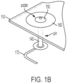
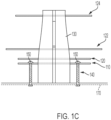
- Conventional high frequency radiator 100 presents the following challenges. First, given four metallic pins 140, each of which are soldered at feed metal pad 160 and corresponding feed line 170, mounting each conventional high frequency radiator 100 to an antenna array face requires eight solder joints. Further, given the height or prominence of solder point 150, and given standard manufacturing variations in soldering, the height of a given solder point 150 may vary by a considerable percentage of the distance between PCB/radiator plate 110 and passive radiator plate 120. These variations in solder point 150 heights may cause considerable impedance mismatches for the conventional high frequency radiator 100. Further, since the center of plates 110/120/122/124 are mounted to a non-conductive supporting pedestal 130, they may be bent. This may cause a change in distance between PCB/radiator plate 110 and passive radiator plate 120.
- non-conductive supporting pedestal 130 In order to assemble one antenna, it requires the non-conductive supporting pedestal 130, four metallic pins 140, PCB/radiator plate 110, and at least one passive radiator plate 120, along with eight solder joints.
- US patent application US2016/285169 A1 describes a radiating element for use in a multiband antenna.
- the radiating element includes first and second dipole arms supported by a feedboard including a balun and first and second matching circuits coupled to the balun.
- US patent No. 6,342,867 B1 describes a multifrequency antenna including first and second dipole pairs symmetrically disposed on a first side of a reflector and configured to be fed with equal power in a relative phase rotation.
- An aspect of the present disclosure involves a radiator for an antenna according to claim 1.
- Another aspect of the present invention involves an antenna according to claim 9 that has a plurality of the high frequency radiators.
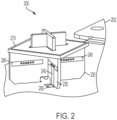
- FIG. 2 illustrates an exemplary high frequency radiator 200, disposed on array face PCB 202.
- High frequency radiator 200 includes a PCB radiator plate 210 that is mounted to two PCB stems 230 that are arranged in an interlocking cross configuration. Disposed on each PCB stem 230 is a feeder metallic trace 240 and an opposing metallic trace 245, each of which is disposed on opposite sides of a corresponding PCB stem 230.
- Feeder metallic trace 240 is coupled to an RF feeder line (not shown) by solder joint 260.
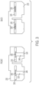
- FIG. 3 illustrates two sides of a PCB stem 230, including a front side and a back side.
- feeder metallic traces 240 Disposed on the front side of PCB stem 230 are feeder metallic traces 240.
- Feeder metallic trace 240 has a vertical feeder portion 320 and a horizontal trace portion 330.
- Opposing metallic trace 245 have a profile (or dimensions) that may substantially overlap with the profile of horizontal trace portion 330 of feeder metallic trace 240.
- a plurality of vias 350 that penetrate the PCB stem 230 and enable the feeder metallic trace 240 and opposing metallic trace 245 to be electrically coupled using solder or another form of electrical connection.
- the vias 350 are disposed horizontally along the profile of horizontal trace portion 330 and opposing metallic trace 245.
- the location of horizontal trace portion 330 and its corresponding opposing metallic trace245 along the vertical dimension may be such that RF current flowing in the combination of horizontal trace portion 330, opposing metallic trace 245, and the solder in the vias 350 may impart RF radiation that couples with PCB radiator plate 210.
- PCB stem 230 is illustrated with both feeder metallic traces 240 on one side and both opposing metallic traces 245 on the other side, it will be readily understood that each combination of feeder metallic trace 240 and opposing metallic trace 245 may be reversed such that one feeder metallic trace 240 may be on one side of PCB stem 230 and the other feeder metallic trace 240 may be on the other side of PCB stem 230.
- PCB stem 230 is illustrated as a single PCB component, PCB stem 230 may be formed of two separate PCB segments, each of which having one combination of feeder metallic trace 240 and opposing metallic trace 245.
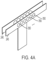
- FIG. 4A illustrates feeder metallic trace 240 and opposing metallic trace 245 disposed on front and back sides of the PCB stems (with the PCB stem structure removed from the illustration), connected by a plurality of conductive traces that are disposed within vias 350 disposed in the PCB stem structure.
- Each combination of traces 240 and 245, coupled through corresponding vias 350, provides sufficient volume of conductive material in the proper configuration and proximity to PCB radiator plate 210 to pump sufficient RF flux into PCB radiator plate 210 for high frequency radiator 200 to function with substantially the same efficiency as conventional high frequency radiator 100, but with fewer components.
- high frequency radiator 200 does not need additional support structures that are required for conventional high frequency radiator 100. Further, high frequency radiator 200 only requires four solder joints 260 as opposed to eight.
- feeder metallic trace 240 and opposing metallic trace 245, and their corresponding vias 350 enables the solder points within vias 350 to be done in such a way that they do not protrude toward PCB radiator plate 210, and thus do not cause imprecision in impedance matching as occurs with conventional high frequency radiator 100.
- the design of high frequency radiator 200 is tolerant of imprecision in soldering.
- FIG. 4B is a "top down" view of feeder metallic trace 240, opposing metallic trace 245, and their corresponding vias 350
- FIG. 4C is a side view of feeder metallic trace240. Both Figures include exemplary dimensions. The length of metallic traces, width of metallic traces, length of vias (PCB substrate thickness), space among vias, and number of vias may be specifically selected in order to obtain the good impedance matching over the desired frequency bands.
- FIG. 5A is a top-down view of the PCB radiator plate 210 of high frequency radiator 200, including metallic plate 510, and a cross aperture 520 through which interlocked PCB stems 230 mechanically engage to support PCB radiator plate 210 and provide mechanical rigidity for high frequency radiator 200.
- FIG. 5B illustrates an alternate embodiment in which a metallic patch 550 is employed in place of PCB radiator plate 210.
- a non-conductive support infrastructure 560 is provided. It will be understood that such variations are possible and within the scope of the disclosure.
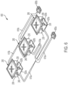
- FIG. 6 illustrates an arrangement of exemplary high frequency radiators 200 as they might be configured on an array face. Illustrated are three high frequency radiators 200 coupled together to two RF signals through RF input ports 605a/b, input feeds 610a/b, fanned-out feeds 615a/b, and phase-split feeds 620a/b. Each RF input signal is fed to a pair of feeder metallic traces 240 on one of PCB stems 230. As illustrated, a given RF input signal is split into two phase-split feeds 620a/b.
- the RF signal presented to one feeder metallic trace 240 on a given PCB stem 230 will be substantially 90 degrees phase shifted to the RF signal presented to the other of front side feeder metallic trace 240 on the same PCB stem 240.
- This enables two features for an antenna: (1) it rotates the polarization vector of the emitted RF signal by 45 degrees; and (2) it enables high frequency radiator 200 to operate in a circular polarization mode, by inputting a single RF signal to both RF inputs 605a/b, but with a 90-degree phase offset between them.
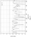
- FIG. 7 is an exemplary measured return loss plot corresponding to the high frequency radiator according to the disclosure
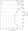
- FIG. 8 is an exemplary measured isolation plot corresponding to the high frequency radiator according to the disclosure, depicting the superior performance of high frequency radiator 200.
- FIG. 9 is an exemplary azimuth radiation pattern plot corresponding to the high frequency radiator according to the disclosure
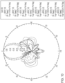
- FIG. 10 is an exemplary azimuth radiation pattern plot corresponding to the high frequency radiator according to the disclosure, depicting the superior performance of high frequency radiator 200.
- the proposed structures shows the good impedance matching and isolation characteristics which are achievable and controllable.
Landscapes
- Engineering & Computer Science (AREA)
- Computer Networks & Wireless Communication (AREA)
- Physics & Mathematics (AREA)
- Electromagnetism (AREA)
- Waveguide Aerials (AREA)
- Variable-Direction Aerials And Aerial Arrays (AREA)
Claims (9)
- Strahler (200) für eine Antenne, umfassend:ein Paar PCB-Arme (230), die in einer ineinandergreifenden Kreuzform angeordnet sind, wobei jeder der PCB-Arme (230) eine Vorderseite und eine Rückseite aufweist, wobei auf jedem PCB-Arm (230) ein Paar metallische Zufuhrspuren (240) angeordnet ist, wobei jede metallische Zufuhrspur einen Zufuhrabschnitt (320) und einen horizontalen Spurabschnitt (330) umfasst, so dass der horizontale Spurabschnitt (330) senkrecht zu dem Zufuhrabschnitt (320) ist, und ein entsprechendes Paar gegenüberliegender metallischer Spuren (245), wobei der horizontale Spurabschnitt ein Profil aufweist, das im Wesentlichen mit einem Profil der korrespondierenden gegenüberliegenden metallischen Spur überlappt, wobei jeder horizontale Spurabschnitt (330) und die korrespondierende gegenüberliegende metallische Spur (245) durch eine Vielzahl von Durchkontaktierungen (350), die in dem PCB-Arm (230) ausgebildet sind, elektrisch gekoppelt sind und wobei die Vielzahl von Durchkontaktierungen (350) horizontal entlang des Profils des horizontalen Spurabschnitts (330) angeordnet ist; undeine Strahlerplatte (210), die mechanisch mit dem Paar von PCB-Armen (230) gekoppelt ist.
- Strahler (200) nach Anspruch 1, wobei die Strahlerplatte (210) umfasst: ein PCB-Substrat; und
eine Metallplatte, die auf dem PCB-Substrat angeordnet ist. - Strahler (200) nach Anspruch 1, wobei die Strahlerplatte (210) umfasst: eine Metallplatte; und
eine nicht leitende Trägerinfrastruktur, mit der die Metallplatte mechanisch gekoppelt ist. - Strahler (200) nach Anspruch 1, wobei das Profil jede metallische Zufuhrspur (240) und gegenüberliegende metallischen Spur (245) eine Länge und eine Breite umfasst, und wobei jede Durchkontaktierung (350) eine Durchkontaktierungslänge aufweist, und wobei die Länge, die Breite, die Durchkontaktierungslänge, ein Abstand zwischen Durchkontaktierungen und eine Anzahl von Durchkontaktierungen ausgewählt sind, um gewünschte Impedanzanpassung über einen Frequenzbereich zu erhalten.
- Strahler (200) nach Anspruch 1, wobei jeder PCB-Arm (230) zwei PCB-Segmente umfasst, wobei jedes PCB-Segment eine Kombination aus der metallischen Zufuhrspur (240) und der korrespondierenden gegenüberliegenden metallischen Spur (245) aufweist.
- Strahler (200) nach Anspruch 1, wobei die Strahlerplatte (210) eine kreuzförmige Öffnung zur mechanischen Befestigung der Strahlerplatte (210) an die PCB-Arme (230) umfasst.
- Strahler (200) nach Anspruch 1, wobei die Kombination der metallischen Zufuhrspur (240) und der korrespondierenden gegenüberliegenden metallischen Spur (245) RF-Fluss zur Strahlerplatte (210) bereitstellt, um RF-Energie abzustrahlen.
- Strahler (200) nach Anspruch 1, wobei die Vielzahl von Durchkontaktierungen (350) parallel zu der Ebene der Strahlerplatte (210) angeordnet sind.
- Antenne, die eine Vielzahl von Strahlern (200) nach einem beliebigen der Ansprüche 1 und 6 - 8 aufweist.
Applications Claiming Priority (2)
| Application Number | Priority Date | Filing Date | Title |
|---|---|---|---|
| US201862671706P | 2018-05-15 | 2018-05-15 | |
| PCT/US2019/032194 WO2019222197A1 (en) | 2018-05-15 | 2019-05-14 | Patch antenna design for easy fabrication and controllable performance at high frequency bands |
Publications (3)
| Publication Number | Publication Date |
|---|---|
| EP3794680A1 EP3794680A1 (de) | 2021-03-24 |
| EP3794680A4 EP3794680A4 (de) | 2022-01-19 |
| EP3794680B1 true EP3794680B1 (de) | 2025-04-23 |
Family
ID=68540950
Family Applications (1)
| Application Number | Title | Priority Date | Filing Date |
|---|---|---|---|
| EP19804318.4A Active EP3794680B1 (de) | 2018-05-15 | 2019-05-14 | Patch-antennen-konstruktion für einfache herstellung und steuerbare leistung bei hochfrequenzbändern |
Country Status (6)
| Country | Link |
|---|---|
| US (1) | US11962095B2 (de) |
| EP (1) | EP3794680B1 (de) |
| KR (1) | KR102804667B1 (de) |
| CN (1) | CN112400256B (de) |
| CA (1) | CA3100197A1 (de) |
| WO (1) | WO2019222197A1 (de) |
Families Citing this family (2)
| Publication number | Priority date | Publication date | Assignee | Title |
|---|---|---|---|---|
| CN113782967B (zh) * | 2021-07-22 | 2023-12-01 | 江苏亨鑫科技有限公司 | 一种免焊接pcb振子装置 |
| US20260121297A1 (en) * | 2024-10-24 | 2026-04-30 | Te Connectivity Solutions Gmbh | High Gain Multiple Input, Multiple Output Antenna |
Family Cites Families (19)
| Publication number | Priority date | Publication date | Assignee | Title |
|---|---|---|---|---|
| US6342867B1 (en) | 2000-03-31 | 2002-01-29 | Navcom Technology, Inc. | Nested turnstile antenna |
| US8102325B2 (en) | 2008-11-10 | 2012-01-24 | Hemisphere Gps Llc | GNSS antenna with selectable gain pattern, method of receiving GNSS signals and antenna manufacturing method |
| MX2011004300A (es) * | 2009-09-14 | 2011-05-30 | World Products Llc | Antenas adaptables-a-medidor optimizadas. |
| TWM398209U (en) * | 2010-08-04 | 2011-02-11 | Wistron Neweb Corp | Broadband antenna |
| KR20120086838A (ko) * | 2011-01-27 | 2012-08-06 | 엘에스전선 주식회사 | Pcb 기판형 광대역 이중 편파 다이폴 안테나 |
| JP5309193B2 (ja) | 2011-07-19 | 2013-10-09 | 電気興業株式会社 | 偏波ダイバーシチアレイアンテナ装置 |
| US9722323B2 (en) | 2012-03-26 | 2017-08-01 | Galtronics Corporation Ltd. | Isolation structures for dual-polarized antennas |
| US20140028516A1 (en) * | 2012-07-25 | 2014-01-30 | Kathrein, Inc., Scala Division | Dual-polarized radiating element with enhanced isolation for use in antenna system |
| US20140049439A1 (en) * | 2012-08-17 | 2014-02-20 | Jimmy Ho | Compact dual-polarized multiple directly fed & em coupled stepped probe element for ultra wideband performance |
| US9276329B2 (en) | 2012-11-22 | 2016-03-01 | Commscope Technologies Llc | Ultra-wideband dual-band cellular basestation antenna |
| CN104868228B (zh) | 2014-02-25 | 2018-05-11 | 华为技术有限公司 | 双极化天线及天线阵列 |
| EP3748772B1 (de) * | 2015-01-15 | 2021-10-13 | CommScope Technologies LLC | Mehrbandige strahlende gruppenantenne mit niedriger gleichtaktresonanz |
| US10128579B2 (en) * | 2015-02-13 | 2018-11-13 | Commscope Technologies Llc | Dipole antenna element with open-end traces |
| CN107851888B (zh) | 2015-06-11 | 2020-09-08 | 科递(上海)贸易有限公司 | 包括多个辐射器的多端口多频带车载天线组件 |
| US9935378B2 (en) * | 2015-10-30 | 2018-04-03 | Te Connectivity Corporation | Antenna apparatus configured to reduce radio-frequency exposure |
| US20180034165A1 (en) * | 2016-03-21 | 2018-02-01 | Zimeng LI | Miniaturized dual-polarized base station antenna |
| US10601120B2 (en) * | 2017-05-17 | 2020-03-24 | Commscope Technologies Llc | Base station antennas having reflector assemblies with RF chokes |
| CN107425268A (zh) | 2017-06-09 | 2017-12-01 | 上海交通大学 | 高增益双模宽带圆极化天线 |
| CN109216911A (zh) * | 2018-09-28 | 2019-01-15 | 深圳国人通信股份有限公司 | 一种双极化辐射单元 |
-
2019
- 2019-05-14 EP EP19804318.4A patent/EP3794680B1/de active Active
- 2019-05-14 CA CA3100197A patent/CA3100197A1/en active Pending
- 2019-05-14 CN CN201980046676.5A patent/CN112400256B/zh active Active
- 2019-05-14 WO PCT/US2019/032194 patent/WO2019222197A1/en not_active Ceased
- 2019-05-14 KR KR1020207036061A patent/KR102804667B1/ko active Active
- 2019-05-14 US US17/054,854 patent/US11962095B2/en active Active
Also Published As
| Publication number | Publication date |
|---|---|
| US20210218157A1 (en) | 2021-07-15 |
| CN112400256B (zh) | 2024-02-02 |
| EP3794680A1 (de) | 2021-03-24 |
| CA3100197A1 (en) | 2019-11-21 |
| CN112400256A (zh) | 2021-02-23 |
| EP3794680A4 (de) | 2022-01-19 |
| US11962095B2 (en) | 2024-04-16 |
| KR20210008866A (ko) | 2021-01-25 |
| WO2019222197A1 (en) | 2019-11-21 |
| KR102804667B1 (ko) | 2025-05-07 |
Similar Documents
| Publication | Publication Date | Title |
|---|---|---|
| US12132264B2 (en) | Integrated filter radiator for a multiband antenna | |
| Chang et al. | Triple-band microstrip patch antenna and its four-antenna module based on half-mode patch for 5G 4× 4 MIMO operation | |
| US10523306B2 (en) | Omnidirectional multiband symmetrical dipole antennas | |
| US8866685B2 (en) | Omnidirectional multi-band antennas | |
| US20220359989A1 (en) | Beam forming antennas having dual-polarized dielectric radiating elements therein | |
| KR102138841B1 (ko) | 안테나 장치 | |
| KR101905507B1 (ko) | 안테나 장치 및 그를 구비하는 전자 기기 | |
| US10797408B1 (en) | Antenna structure and method for manufacturing the same | |
| CN104685714A (zh) | 贴片天线 | |
| JP2004201281A (ja) | 無線lanアンテナ及びこれを具備した無線lanカード | |
| US20030112200A1 (en) | Horizontally polarized printed circuit antenna array | |
| CN116325360A (zh) | 具有支持高频带掩蔽的紧凑双极化盒形偶极子辐射元件的基站天线 | |
| US10707582B2 (en) | Wide-band dipole antenna | |
| KR100795485B1 (ko) | 광대역 다이폴 안테나 | |
| EP3794680B1 (de) | Patch-antennen-konstruktion für einfache herstellung und steuerbare leistung bei hochfrequenzbändern | |
| US20240421494A1 (en) | Base station antennas having compact dual-polarized box dipole radiating elements therein that support high band cloaking | |
| TW201208197A (en) | High gain loop array antenna system and electronic device | |
| JP7158606B2 (ja) | アンテナ装置および無線通信機能付きセンサ | |
| CN117638466A (zh) | 天线模组、天线阵列及电子设备 | |
| US20260058371A1 (en) | Folded antenna dipole with on-substrate passive radiators | |
| KR100723682B1 (ko) | 단말기용 삼중대역 cpw급전 평면 역f형 안테나 | |
| WO2024230932A1 (en) | Electrically conductive grounding structure for a multi-band antenna | |
| CN121922865A (zh) | 高增益多输入多输出天线 | |
| JP2020108050A (ja) | アンテナ装置および無線端末 |
Legal Events
| Date | Code | Title | Description |
|---|---|---|---|
| STAA | Information on the status of an ep patent application or granted ep patent |
Free format text: STATUS: THE INTERNATIONAL PUBLICATION HAS BEEN MADE |
|
| PUAI | Public reference made under article 153(3) epc to a published international application that has entered the european phase |
Free format text: ORIGINAL CODE: 0009012 |
|
| STAA | Information on the status of an ep patent application or granted ep patent |
Free format text: STATUS: REQUEST FOR EXAMINATION WAS MADE |
|
| 17P | Request for examination filed |
Effective date: 20201117 |
|
| AK | Designated contracting states |
Kind code of ref document: A1 Designated state(s): AL AT BE BG CH CY CZ DE DK EE ES FI FR GB GR HR HU IE IS IT LI LT LU LV MC MK MT NL NO PL PT RO RS SE SI SK SM TR |
|
| AX | Request for extension of the european patent |
Extension state: BA ME |
|
| DAV | Request for validation of the european patent (deleted) | ||
| DAX | Request for extension of the european patent (deleted) | ||
| A4 | Supplementary search report drawn up and despatched |
Effective date: 20211216 |
|
| RIC1 | Information provided on ipc code assigned before grant |
Ipc: H01Q 1/24 20060101ALI20211210BHEP Ipc: H01Q 21/26 20060101ALI20211210BHEP Ipc: H01Q 21/08 20060101ALI20211210BHEP Ipc: H01Q 9/04 20060101AFI20211210BHEP |
|
| STAA | Information on the status of an ep patent application or granted ep patent |
Free format text: STATUS: EXAMINATION IS IN PROGRESS |
|
| 17Q | First examination report despatched |
Effective date: 20230116 |
|
| GRAP | Despatch of communication of intention to grant a patent |
Free format text: ORIGINAL CODE: EPIDOSNIGR1 |
|
| STAA | Information on the status of an ep patent application or granted ep patent |
Free format text: STATUS: GRANT OF PATENT IS INTENDED |
|
| INTG | Intention to grant announced |
Effective date: 20241119 |
|
| GRAS | Grant fee paid |
Free format text: ORIGINAL CODE: EPIDOSNIGR3 |
|
| GRAA | (expected) grant |
Free format text: ORIGINAL CODE: 0009210 |
|
| STAA | Information on the status of an ep patent application or granted ep patent |
Free format text: STATUS: THE PATENT HAS BEEN GRANTED |
|
| AK | Designated contracting states |
Kind code of ref document: B1 Designated state(s): AL AT BE BG CH CY CZ DE DK EE ES FI FR GB GR HR HU IE IS IT LI LT LU LV MC MK MT NL NO PL PT RO RS SE SI SK SM TR |
|
| REG | Reference to a national code |
Ref country code: GB Ref legal event code: FG4D |
|
| REG | Reference to a national code |
Ref country code: CH Ref legal event code: EP |
|
| REG | Reference to a national code |
Ref country code: DE Ref legal event code: R096 Ref document number: 602019069057 Country of ref document: DE |
|
| REG | Reference to a national code |
Ref country code: IE Ref legal event code: FG4D |
|
| PGFP | Annual fee paid to national office [announced via postgrant information from national office to epo] |
Ref country code: DE Payment date: 20250528 Year of fee payment: 7 |
|
| PGFP | Annual fee paid to national office [announced via postgrant information from national office to epo] |
Ref country code: GB Payment date: 20250522 Year of fee payment: 7 |
|
| PGFP | Annual fee paid to national office [announced via postgrant information from national office to epo] |
Ref country code: FR Payment date: 20250623 Year of fee payment: 7 |
|
| REG | Reference to a national code |
Ref country code: NL Ref legal event code: MP Effective date: 20250423 |
|
| PG25 | Lapsed in a contracting state [announced via postgrant information from national office to epo] |
Ref country code: NL Free format text: LAPSE BECAUSE OF FAILURE TO SUBMIT A TRANSLATION OF THE DESCRIPTION OR TO PAY THE FEE WITHIN THE PRESCRIBED TIME-LIMIT Effective date: 20250423 |
|
| REG | Reference to a national code |
Ref country code: AT Ref legal event code: MK05 Ref document number: 1788740 Country of ref document: AT Kind code of ref document: T Effective date: 20250423 |
|
| PG25 | Lapsed in a contracting state [announced via postgrant information from national office to epo] |
Ref country code: PT Free format text: LAPSE BECAUSE OF FAILURE TO SUBMIT A TRANSLATION OF THE DESCRIPTION OR TO PAY THE FEE WITHIN THE PRESCRIBED TIME-LIMIT Effective date: 20250825 Ref country code: ES Free format text: LAPSE BECAUSE OF FAILURE TO SUBMIT A TRANSLATION OF THE DESCRIPTION OR TO PAY THE FEE WITHIN THE PRESCRIBED TIME-LIMIT Effective date: 20250423 Ref country code: FI Free format text: LAPSE BECAUSE OF FAILURE TO SUBMIT A TRANSLATION OF THE DESCRIPTION OR TO PAY THE FEE WITHIN THE PRESCRIBED TIME-LIMIT Effective date: 20250423 |
|
| REG | Reference to a national code |
Ref country code: LT Ref legal event code: MG9D |
|
| PG25 | Lapsed in a contracting state [announced via postgrant information from national office to epo] |
Ref country code: GR Free format text: LAPSE BECAUSE OF FAILURE TO SUBMIT A TRANSLATION OF THE DESCRIPTION OR TO PAY THE FEE WITHIN THE PRESCRIBED TIME-LIMIT Effective date: 20250724 Ref country code: NO Free format text: LAPSE BECAUSE OF FAILURE TO SUBMIT A TRANSLATION OF THE DESCRIPTION OR TO PAY THE FEE WITHIN THE PRESCRIBED TIME-LIMIT Effective date: 20250723 |
|
| PG25 | Lapsed in a contracting state [announced via postgrant information from national office to epo] |
Ref country code: PL Free format text: LAPSE BECAUSE OF FAILURE TO SUBMIT A TRANSLATION OF THE DESCRIPTION OR TO PAY THE FEE WITHIN THE PRESCRIBED TIME-LIMIT Effective date: 20250423 |
|
| PGFP | Annual fee paid to national office [announced via postgrant information from national office to epo] |
Ref country code: IT Payment date: 20250613 Year of fee payment: 7 |
|
| PG25 | Lapsed in a contracting state [announced via postgrant information from national office to epo] |
Ref country code: BG Free format text: LAPSE BECAUSE OF FAILURE TO SUBMIT A TRANSLATION OF THE DESCRIPTION OR TO PAY THE FEE WITHIN THE PRESCRIBED TIME-LIMIT Effective date: 20250423 |
|
| PG25 | Lapsed in a contracting state [announced via postgrant information from national office to epo] |
Ref country code: HR Free format text: LAPSE BECAUSE OF FAILURE TO SUBMIT A TRANSLATION OF THE DESCRIPTION OR TO PAY THE FEE WITHIN THE PRESCRIBED TIME-LIMIT Effective date: 20250423 |
|
| PG25 | Lapsed in a contracting state [announced via postgrant information from national office to epo] |
Ref country code: AT Free format text: LAPSE BECAUSE OF FAILURE TO SUBMIT A TRANSLATION OF THE DESCRIPTION OR TO PAY THE FEE WITHIN THE PRESCRIBED TIME-LIMIT Effective date: 20250423 |
|
| PG25 | Lapsed in a contracting state [announced via postgrant information from national office to epo] |
Ref country code: RS Free format text: LAPSE BECAUSE OF FAILURE TO SUBMIT A TRANSLATION OF THE DESCRIPTION OR TO PAY THE FEE WITHIN THE PRESCRIBED TIME-LIMIT Effective date: 20250723 |
|
| PG25 | Lapsed in a contracting state [announced via postgrant information from national office to epo] |
Ref country code: IS Free format text: LAPSE BECAUSE OF FAILURE TO SUBMIT A TRANSLATION OF THE DESCRIPTION OR TO PAY THE FEE WITHIN THE PRESCRIBED TIME-LIMIT Effective date: 20250823 |
|
| PG25 | Lapsed in a contracting state [announced via postgrant information from national office to epo] |
Ref country code: LV Free format text: LAPSE BECAUSE OF FAILURE TO SUBMIT A TRANSLATION OF THE DESCRIPTION OR TO PAY THE FEE WITHIN THE PRESCRIBED TIME-LIMIT Effective date: 20250423 |
|
| REG | Reference to a national code |
Ref country code: CH Ref legal event code: H13 Free format text: ST27 STATUS EVENT CODE: U-0-0-H10-H13 (AS PROVIDED BY THE NATIONAL OFFICE) Effective date: 20251223 |
|
| PG25 | Lapsed in a contracting state [announced via postgrant information from national office to epo] |
Ref country code: DK Free format text: LAPSE BECAUSE OF FAILURE TO SUBMIT A TRANSLATION OF THE DESCRIPTION OR TO PAY THE FEE WITHIN THE PRESCRIBED TIME-LIMIT Effective date: 20250423 Ref country code: SM Free format text: LAPSE BECAUSE OF FAILURE TO SUBMIT A TRANSLATION OF THE DESCRIPTION OR TO PAY THE FEE WITHIN THE PRESCRIBED TIME-LIMIT Effective date: 20250423 |
|
| PG25 | Lapsed in a contracting state [announced via postgrant information from national office to epo] |
Ref country code: LU Free format text: LAPSE BECAUSE OF NON-PAYMENT OF DUE FEES Effective date: 20250514 |
|
| PG25 | Lapsed in a contracting state [announced via postgrant information from national office to epo] |
Ref country code: CH Free format text: LAPSE BECAUSE OF NON-PAYMENT OF DUE FEES Effective date: 20250531 |
|
| PG25 | Lapsed in a contracting state [announced via postgrant information from national office to epo] |
Ref country code: CZ Free format text: LAPSE BECAUSE OF FAILURE TO SUBMIT A TRANSLATION OF THE DESCRIPTION OR TO PAY THE FEE WITHIN THE PRESCRIBED TIME-LIMIT Effective date: 20250423 |
|
| PG25 | Lapsed in a contracting state [announced via postgrant information from national office to epo] |
Ref country code: EE Free format text: LAPSE BECAUSE OF FAILURE TO SUBMIT A TRANSLATION OF THE DESCRIPTION OR TO PAY THE FEE WITHIN THE PRESCRIBED TIME-LIMIT Effective date: 20250423 |
|
| REG | Reference to a national code |
Ref country code: DE Ref legal event code: R097 Ref document number: 602019069057 Country of ref document: DE |
|
| PG25 | Lapsed in a contracting state [announced via postgrant information from national office to epo] |
Ref country code: RO Free format text: LAPSE BECAUSE OF FAILURE TO SUBMIT A TRANSLATION OF THE DESCRIPTION OR TO PAY THE FEE WITHIN THE PRESCRIBED TIME-LIMIT Effective date: 20250423 Ref country code: SK Free format text: LAPSE BECAUSE OF FAILURE TO SUBMIT A TRANSLATION OF THE DESCRIPTION OR TO PAY THE FEE WITHIN THE PRESCRIBED TIME-LIMIT Effective date: 20250423 |
|
| REG | Reference to a national code |
Ref country code: BE Ref legal event code: MM Effective date: 20250531 |
|
| PG25 | Lapsed in a contracting state [announced via postgrant information from national office to epo] |
Ref country code: MC Free format text: LAPSE BECAUSE OF FAILURE TO SUBMIT A TRANSLATION OF THE DESCRIPTION OR TO PAY THE FEE WITHIN THE PRESCRIBED TIME-LIMIT Effective date: 20250423 |
|
| PLBE | No opposition filed within time limit |
Free format text: ORIGINAL CODE: 0009261 |
|
| STAA | Information on the status of an ep patent application or granted ep patent |
Free format text: STATUS: NO OPPOSITION FILED WITHIN TIME LIMIT |
|
| REG | Reference to a national code |
Ref country code: CH Ref legal event code: L10 Free format text: ST27 STATUS EVENT CODE: U-0-0-L10-L00 (AS PROVIDED BY THE NATIONAL OFFICE) Effective date: 20260304 |
|
| 26N | No opposition filed |
Effective date: 20260126 |
|
| PG25 | Lapsed in a contracting state [announced via postgrant information from national office to epo] |
Ref country code: IE Free format text: LAPSE BECAUSE OF NON-PAYMENT OF DUE FEES Effective date: 20250514 |
|
| PG25 | Lapsed in a contracting state [announced via postgrant information from national office to epo] |
Ref country code: BE Free format text: LAPSE BECAUSE OF NON-PAYMENT OF DUE FEES Effective date: 20250531 |