EP3796013B1 - Zur aufnahme einer radiofrequenzsonde zum testen einer elektrischen vorrichtung konfigurierte schnittstelle und verfahren zum testen einer auf einem substrat angeordneten elektrischen vorrichtung - Google Patents
Zur aufnahme einer radiofrequenzsonde zum testen einer elektrischen vorrichtung konfigurierte schnittstelle und verfahren zum testen einer auf einem substrat angeordneten elektrischen vorrichtung Download PDFInfo
- Publication number
- EP3796013B1 EP3796013B1 EP19198097.8A EP19198097A EP3796013B1 EP 3796013 B1 EP3796013 B1 EP 3796013B1 EP 19198097 A EP19198097 A EP 19198097A EP 3796013 B1 EP3796013 B1 EP 3796013B1
- Authority
- EP
- European Patent Office
- Prior art keywords
- conductive structure
- capacitive element
- electric device
- substrate
- interface
- Prior art date
- Legal status (The legal status is an assumption and is not a legal conclusion. Google has not performed a legal analysis and makes no representation as to the accuracy of the status listed.)
- Active
Links
Images


Classifications
-
- G—PHYSICS
- G01—MEASURING; TESTING
- G01R—MEASURING ELECTRIC VARIABLES; MEASURING MAGNETIC VARIABLES
- G01R31/00—Arrangements for testing electric properties; Arrangements for locating electric faults; Arrangements for electrical testing characterised by what is being tested not provided for elsewhere
- G01R31/28—Testing of electronic circuits, e.g. by signal tracer
- G01R31/2851—Testing of integrated circuits [IC]
- G01R31/2884—Testing of integrated circuits [IC] using dedicated test connectors, test elements or test circuits on the IC under test
-
- G—PHYSICS
- G01—MEASURING; TESTING
- G01R—MEASURING ELECTRIC VARIABLES; MEASURING MAGNETIC VARIABLES
- G01R31/00—Arrangements for testing electric properties; Arrangements for locating electric faults; Arrangements for electrical testing characterised by what is being tested not provided for elsewhere
- G01R31/28—Testing of electronic circuits, e.g. by signal tracer
- G01R31/282—Testing of electronic circuits specially adapted for particular applications not provided for elsewhere
- G01R31/2822—Testing of electronic circuits specially adapted for particular applications not provided for elsewhere of microwave or radiofrequency circuits
Definitions
- Examples relate to testing electric devices using Radio Frequency (RF) probes.
- examples relate to an electric system comprising an electric device arranged on a substrate.
- Further examples relate to a method for testing an electric device arranged on a substrate.
- RF Radio Frequency
- Document JP 2018 137296 A proposes a high frequency device suppressed in deterioration of high frequency characteristics due to a pad. Further, document US 2015/145098 A1 proposes a miniature passive structure for electrostatic discharge protection.
- RF measurement of test devices on a system board requires so called launch structures (also known as launchers) for providing interconnection between RF probes and transmission lines on the board.
- launch structures also known as launchers
- a launcher should be broadband and "transparent" for the measured signals. In other words, it should not introduce signal losses and signal reflections at the interface of the RF probe and the board.
- An example relates to an electric system.
- the electric system comprises an electric device arranged on a substrate. Further, the electric device comprises an interface arranged on the substrate and adapted to receive a RF probe for testing the electric device.
- the interface comprises a first conductive structure for receiving at least one probe tip of the RF probe.
- the first conductive structure is coupled to a signal line in or on the substrate that couples to the electric device.
- the interface comprises a second conductive structure for receiving at least one further probe tip of the RF probe; said second conductive structure being electrically coupled to the electric device by one or more vias of the substrate, in order to provide a reference signal to said electric device.
- the interface additionally comprises a capacitive element for providing a compensation capacitance.
- the capacitive element and the first conductive structure are electrically coupled in order to form a compensation network for compensating RF parasitics.
- the first conductive structure extends lengthwise along a spatial axis.
- the capacitive element and the signal line are arranged on opposite sides of the first conductive structure along the spatial axis.
- the capacitive element comprises a MEMS capacitor configured to receive one or more control signals for adjusting an adjustable capacitance of the MEMS capacitor.
- a further example relates to a method for testing an electric device arranged on a substrate.
- the method comprises placing a RF probe onto an interface arranged on the substrate such that a first conductive structure of the interface receives at least one probe tip of the RF probe and that a second conductive structure of the interface receives at least one further probe tip of the RF probe; said second conductive structure being electrically coupled to the electric device by one or more vias of the substrate, in order to provide a reference signal to said electric device.
- the first conductive structure is coupled to a signal line in or on the substrate that couples to the electric device.
- the first conductive structure and a capacitive element for providing a compensation capacitance are electrically coupled in order to form a compensation network for compensating RF parasitics.
- the first conductive structure extends lengthwise along a spatial axis.
- the capacitive element and the signal line are arranged on opposite sides of the first conductive structure along the spatial axis.
- the capacitive element comprises a MEMS capacitor exhibiting an adjustable capacitance.
- the method further comprises supplying one or more control signals to the MEMS capacitor for adjusting the adjustable capacitance of the MEMS capacitor.
- the method additionally comprises applying a test signal to the interface via the at least one probe tip.
- Fig. 1 illustrates an example of an interface 100 adapted to receive a RF probe (not illustrated) for testing an electric device (not illustrated) that is arranged on a same (test) substrate 199 as the interface 100.
- the substrate 199 serves as a substrate for the electric device and the interface 100.
- the substrate 199 may be a Printed Circuit Board (PCB) or a glass substrate.
- the electric device may be understood as a Device Under Test (DUT). It is to be noted that the electric device may be mounted on the substrate 199 or be embedded within the substrate 199.
- the RF probe may, e.g., be a Ground-Signal-Ground (GSG) probe for RF testing the electric device.
- GSG Ground-Signal-Ground
- the interface comprises a first conductive structure 110 for receiving at least one probe tip of the RF probe, and a second conductive structure 120 for receiving at least one further probe tip of the RF probe.
- the first conductive structure 110 and the second conductive structure 120 may be coplanar, i.e. be arranged in a same layer. Alternatively, the first conductive structure 110 and the second conductive structure 120 may be arranged in different layers.
- the first conductive structure 110 and the second conductive structure 120 may, e.g., be metal structures.
- the second conductive structure 120 is for receiving a reference signal from the at least one further probe tip of the RF probe (e.g. a ground reference from two further probe tips of the RF probe).
- the second conductive structure 120 electrically couples to the electric device by one or more vias of the substrate.
- the second conductive structure 120 electrically couples to four vias 101, 102, 103 and 104.
- the electric device may be coupled to a defined reference signal (e.g. a reference ground) while measuring/characterizing the electric device by means of the RF probe.
- the first conductive structure 110 is for receiving a test signal from the at least one probe tip of the RF probe.
- the at least one probe tip is used to apply a test signal to the interface 100 and, hence, the electric device. Therefore, the first conductive structure 110 is coupled at a first end 111 to a signal line 150 on the substrate 199 that couples to the electric device. In other words, the first conductive structure 110 is coupled to the electric device via the signal line 150.
- the signal line 150 is a conductive path routed on the substrate (e.g. the surface of the substrate).
- the signal line 150 may be a MicroStrip Line (MSL).
- GSG probe is merely an example for an RF probe.
- any type of RF probe may be used.
- an RF probe comprising only a probe tip for applying a test signal to the first conductive structure 110, and only one other probe tip for applying a reference signal to the second conductive structure 120 may be used.
- one or more additional signal lines e.g. coplanar to transmission line 150 may be used for coupling the second conductive structure 120 to the electric device instead of the vias illustrated in Fig. 1 .
- the first conductive structure 110 is for instance strip-shaped.
- strip-shaped is to be understood such that a dimension (extension) of an element such as first conductive structure 110 along a spatial axis is much greater (e.g. at least two, three, four, five, ten, twenty, fifty or one hundred times greater) than a dimension of the element along another spatial axis which is orthogonal to the spatial axis.
- the first conductive structure 110 extends lengthwise along a spatial axis x such that the dimension of the first conductive structure 110 along the spatial axis x is much greater than the dimension of the first conductive structure 110 along the other spatial axis y which is orthogonal to the spatial axis x .
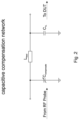
- any conductive structure or material forming the signal path between the signal line 150 and the position at which the RF probe is placed on (touches) the first conductive structure 110 leads to a (small) series inductance L feed (see Fig. 2 ).
- part of the first conductive structure 110 as well as the short interconnection 170 between the first conductive structure 110 and the signal line 150 may cause the series inductance L feed in the example of Fig. 1 .
- the series inductance together with the capacitance C TL of the signal line 150 causes unwanted RF parasitics at the interface.
- RF parasitics become especially problematic when the dimensions of the interface 100 and/or the probe have an order of magnitude which is close or equal to that of the wavelength of the test signal (e.g. when they differ from two orders of magnitude or less or are of the same order of magnitude).
- the interface 100 further comprises a capacitive element 140 for providing a compensation capacitance C compensate .
- the capacitive element 140 and the first conductive structure 110 are electrically coupled in order to form a compensation network for compensating the RF parasitics.
- the capacitive element 140 is not in electrical contact with the second conductive structure 120 since the capacitive element 140 does not touch the second conductive structure 120.
- the capacitive element 140 electrically couples (is attached) to a second end 112 of the first conductive structure 110.
- the capacitive element 140 and the signal line 150 are arranged on opposite sides of each of the first conductive structure 110 along the spatial axis x . In other words, a compensation capacitance C compensate is added at the RF probe side of the structure illustrated in Fig. 1 .
- FIG. 2 An equivalent circuit of the example depicted in Fig. 1 is illustrated in Fig. 2 .
- the inherent capacitance of the signal line 150 is represented by the capacitance C TL .
- the capacitive element 140 adds a compensation capacitance C compensate such that the series inductance L feed and the compensation capacitance C compensate of the capacitive element 140 form an LC compensation network that allows to compensate at least in part for the unwanted RF parasitics caused by the series inductance L feed and the capacitance C TL of the signal line 150.
- the compensation capacitance C compensate of the capacitive element 140 may allow to compensate for the series inductance L feed .
- the compensation capacitance C com-pensate of the capacitive element 140 may allow for a significantly increased bandwidth of the interface 100 compared to conventional launcher structures.
- the proposed incorporation of an LC compensation network into the launcher structure may allow to compensate for RF probe-to-substrate transition related parasitics.
- the second conductive structure 120 is formed integrally such that end portions 121 and 122 of the second conductive structure 120 are arranged on opposite sides of the spatial axis x .
- the second conductive structure 120 defines an inner space 130 within which the capacitive element 140 is arranged. All or part of the first conductive structure 110 may also be arranged within the inner space 130.
- the shape of the second conductive structure 120 is symmetrical with respect to the spatial axis x . It is to be noted that the respective locations of the vias 101, ... , 104 need not be symmetrical with respect to the spatial axis x . In alternative examples, the shape of the second conductive structure 120 may be asymmetrical with respect to the spatial axis x .
- the capacitive element 140 may be implemented in many different ways.
- the capacitive element 140 may be implemented with a fixed, predetermined capacitance or with an adjustable capacitance (e.g. depending on the frequency of the test signal to be applied via the first conductive structure 110).
- the capacitive element 140 is a metal pad (patch) of a predefined capacitance (e.g. the desired compensation capacitance C compensate ).
- the capacitive element 140 may alternatively be formed by any other suitable electrically conductive material such as electrically conductive ceramics.
- the metal pad is irregularly shaped.
- the capacitive element 140 may, in general, be of arbitrary shape. In other examples, the capacitive element may be of rectangular shape as indicated by the capacitive element 340 of interface 300 illustrated in Fig. 3 . In alternative examples, the capacitive element may be of circular shape as indicated by the capacitive element 440 of interface 400 illustrated in Fig. 4 .
- the second conductive structure 120 is not formed integrally, i.e. the second conductive structure 120 does not consist of a single conductive element.
- the second conductive structures of the interfaces 300 and 400 each comprise a first sub-structure 123 and a second sub-structure 124.
- the first and the second sub-structure 123, 124 are arranged on opposite sides of the spatial axis x and are electrically separated from each other.
- the capacitive element 140 is not in electrical contact with the first and the second sub-structure 123, 124 forming the second conductive structure as the capacitive element 140 does not touch the first and the second sub-structure 123, 124.
- shapes of the first and the second sub-structure 123, 124 may be symmetrical with respect to the spatial axis x .
- the shapes of the first and the second sub-structure 123, 124 may be asymmetrical with respect to the spatial axis x .
- one of the first and the second sub-structure 123, 124 may be cut in order to have the shape of the respective sub-structure fit the position in which it needs to be placed. Symmetrical shapes may enable better performance, but are not necessary.
- the integrally-formed second conductive structure 120 illustrated in Fig. 1 Similarly, the vias 101 to 104 may be placed in a non-symmetric manner, as indicated above.
- the first conductive structure 110 presents an extending portion 113 that extends along the spatial axis x beyond vertical projections of the first and the second sub-structure 123, 124 onto the spatial axis x .
- the vertical projections of the first and the second sub-structure 123, 124 onto the spatial axis x are indicated by dashed lines 125 and 126 in Fig. 5 .
- At least part of the extending portion 113 forms the capacitive element 540.
- the first conductive structure 110 is prolonged in order to provide a capacitive element 540 with the desired compensation capacitance C compen-sate at an opposite end of the first conductive structure 110 compared to the interconnection 170 to the signal line 150.
- the capacitive element may be a lengthwise prolongation of the first conductive structure 110, whose dimension along the spatial axis is chosen so that the compensation capacitance exhibits a target value.
- the capacitive element may be (comprise) a (active) MEMS capacitor as illustrated in Fig. 6.
- Fig. 6 illustrates another interface 600 comprising a MEMS capacitor 640 coupled to the second end 112 of the first conductive structure 110.
- a MEMS capacitor is a capacitor manufactured in MicroElectroMechanical Systems (MEMS) technology.
- a distance (gap) between electrodes of the MEMS capacitor 640 is adjustable based on one or more control signals 641 (e.g. the number of control signal may depend on the implementation of the MEMS capacitor 640) for adjusting a capacitance of the MEMS capacitor 640 (e.g. to the desired compensation capacitance C compensate ).
- the MEMS capacitor 640 is configured to receive one or more control signals 641 for adjusting an adjustable capacitance of the MEMS capacitor 640 (e.g. the MEMS capacitance may be adjusted via DC biasing).
- the position of the RF probe along the longitudinal extension of the first conductive structure 110 may be varied to fine-tune the compensation capacitance.
- the position of the RF probe, i.e. the probe tips, on the interface is indicated by line 160 in Figs. 3 to 6 .
- the compensation capacitance C compen-sate effectively seen by the RF probe may be fine-tuned.
- the smart grounding concept indicated by the arrows 161 and 162 may allow a fine-adjustment of the compensation capacitance.
- the first conductive structure 110 is substantially strip-shaped.
- the first conductive structure 110 may in general exhibit any shape.
- An example of a dumbbell-shaped first conductive structure 110 is illustrated in Fig. 7.
- Fig. 7 illustrates another interface 700 comprising the dumbbell-shaped first conductive structure 110.
- Fig. 7 illustrates that the individual elements of an interface according to the proposed technique may be arranged in different layers on the substrate.
- the first conductive structure 110 and the sub-structure 123, 124 of the second conductive structure are arranged in the same layer (i.e. they are coplanar).
- the capacitive element 740 and the signal line 150 are arranged in two other layers.
- the first conductive structure 110 is in electrical contact with the capacitive element 740 and the signal line 150 via respective vias 105 and 106.
- Fig. 7 additionally illustrates that the number of vias coupled to the second conductive structure may be arbitrarily chosen. While in each of the examples described above in connection with Figs. 1 and 3 to 6 four vias are coupled to the second conductive structure, only two vias are coupled to the sub-structures 123 and 124 forming the second conductive structure. Also the shape of the sub-structures 123 and 124 varies compared to the examples described above in connection with Figs. 3 to 6 . It is to be noted that the shapes of the sub-structures 123 and 124 may be chosen freely according to the proposed concept.
- Fig. 8 illustrates an exemplary comparison of the reflection losses for an interface according to the proposed technique and a conventional launcher structure.
- the reflection loss for the interface according to the proposed technique is indicated by scattering parameter S 11 denoting the ratio between the signal power reflected by the interface and the signal power input to the interface.
- Line 810 represents the course of the scattering parameter S 11 for the interface over an exemplary frequency range from 0 GHz to 110 GHz. It is to be noted that the proposed LC compensation network is not limited to the exemplary frequency range illustrated in Fig. 8 . In general, the proposed LC compensation network may be used for any frequency range.
- the reflection loss for a conventional launcher structure at a frequency of 80 GHz is indicated in Fig. 8 by means of double arrow 820.
- a conventional launcher structure typically shows a reflection loss of about -5 to -10 dB as indicated by the double arrow 820.
- the proposed interface shows a reflection loss of about -19 dB. That is, the proposed interface is more "transparent" for measurement signals than a conventional launcher structure. Further, Fig. 8 shows that the reflection loss is well below -15 dB over the whole exemplary frequency range from 0 GHz to 110 GHz. The low reflection loss helps achieving a low insertion loss. Therefore, the proposed interface may allow broadband RF measurement/characterization of an electronic device with high performance (i.e. higher measurement accuracy).
- An electric system comprising an electric device and an interface according to the proposed concept arranged on the same substrate may allow broadband RF measurement/characterization of the electronic device with high performance.
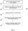
- Method 900 comprises placing 902 a RF probe onto an interface as described above.
- method 900 comprises placing 902 a RF probe onto an interface arranged on the substrate such that a first conductive structure of the interface receives at least one probe tip of the RF probe and that a second conductive structure of the interface receives at least one further probe tip of the RF probe.
- the first conductive structure is coupled to a signal line on the substrate that couples to the electric device.
- the first conductive structure and a capacitive element for providing a compensation capacitance are electrically coupled in order to form a compensation network for compensating RF parasitics.
- Method 900 additionally comprises applying 904 a test signal to the interface via the at least one probe tip.
- method 900 may allow to overcome RF parasitics over a wide frequency range. Accordingly, method 900 may allow broadband RF measurement/characterization of the electronic device with high performance, i.e. low signal loss and signal reflections at the interface between the RF probe and the substrate.
- Method 900 may, hence, comprise varying 906 a position of the RF probe along a longitudinal extension of the first conductive structure.
- method 900 may additionally comprise supplying 908 one or more control signals to the MEMS capacitor for adjusting the adjustable capacitance of the MEMS capacitor (e.g. to a predefined capacitance).
- method 900 may optionally further comprise applying 910 a reference signal to the interface via the at least one further probe tip.
- Method 900 may comprise one or more additional optional features corresponding to one or more aspects of the proposed technique or one or more examples described above.
- FIG. 10 An exemplary set-up for a GSG measurement according to method 900 is illustrated in Fig. 10 .
- a RF probe 1010 is placed onto interface 1020 as described above in connection with Fig. 4 .
- a first conductive structure 1021 of the interface receives the probe tip 1011 of the RF probe 1010.
- the second conductive structure of the interface 1020 comprises a first sub-structure 1022 and a second sub-structure 1023.
- Each of the first sub-structure 1022 and the second sub-structure 1023 receives a respective one of the further probe tips 1012 and 1013 of the RF probe 1010.
- a test signal is applied to the interface 1020 via the probe tip 1011, wherein a ground reference (as an example of a reference signal) is applied to the interface via the further probe tips 1012 and 1013.
- the test signal and the ground reference is supplied to an electric device under test via the interface 1020 in accordance with method 900.
- Some examples relate to an interface adapted to receive a RF probe for testing an electric device that is arranged on a same substrate as the interface.
- the interface comprises a first conductive structure for receiving at least one probe tip of the RF probe.
- the first conductive structure is coupled to a signal line in or on the substrate that couples to the electric device.
- the interface comprises a second conductive structure for receiving at least one further probe tip of the RF probe.
- the interface additionally comprises a capacitive element for providing a compensation capacitance.
- the capacitive element and the first conductive structure are electrically coupled in order to form a compensation network for compensating RF parasitics.
- the capacitive element is not in electrical contact with the second conductive structure.
- the first conductive structure extends lengthwise along a spatial axis, wherein the capacitive element and the signal line are arranged on opposite sides of the first conductive structure along the spatial axis.
- the second conductive structure defines an inner space within which the capacitive element is arranged.
- the second conductive structure is formed integrally such that end portions of the second conductive structure are arranged on opposite sides of the spatial axis.
- the second conductive structure comprises a first sub-structure and a second sub-structure, wherein the first and the second sub-structure are arranged on opposite sides of the spatial axis and are electrically separated from each other.
- shapes of the first and the second sub-structure are symmetrical with respect to the spatial axis.
- shapes of the first and the second sub-structure are asymmetrical with respect to the spatial axis.
- the first conductive structure presents an extending portion that extends along the spatial axis beyond vertical projections of the first and the second sub-structure onto the spatial axis, wherein at least part of the extending portion forms the capacitive element.
- the capacitive element is a pad of electrically conductive material.
- the capacitive element comprises a MEMS capacitor configured to receive one or more control signals for adjusting an adjustable capacitance of the MEMS capacitor.
- the first conductive structure and the second conductive structure are coplanar.
- the second conductive structure electrically couples to one or more vias of the substrate coupled to the electric device.
- Another example relates to an electric system comprising an electric device arranged on a substrate, and an interface as described herein which is arranged on the substrate.
- a further example relates to a method for testing an electric device arranged on a substrate.
- the method comprises placing a RF probe onto an interface arranged on the substrate such that a first conductive structure of the interface receives at least one probe tip of the RF probe and that a second conductive structure of the interface receives at least one further probe tip of the RF probe.
- the first conductive structure is coupled to a signal line on the substrate that couples to the electric device.
- the first conductive structure and a capacitive element for providing a compensation capacitance are electrically coupled in order to form a compensation network for compensating RF parasitics.
- the method additionally comprises applying a test signal to the interface via the at least one probe tip.
- the method further comprises varying a position of the at least one probe tip along a longitudinal extension of the first conductive structure.
- the capacitive element comprises a MEMS capacitor exhibiting an adjustable capacitance
- the method further comprises supplying one or more control signals to the MEMS capacitor for adjusting the adjustable capacitance of the MEMS capacitor.
- the method further comprises applying a reference signal to the interface via the at least one further probe tip.
- Examples according to the proposed technique may allow to overcome parasitics of an RF probe interface by usage of an LC compensation network.
- a block diagram may, for instance, illustrate a high-level circuit diagram implementing the principles of the disclosure.
- Methods disclosed in the specification or in the claims may be implemented by a device having means for performing each of the respective acts of these methods.
Landscapes
- Engineering & Computer Science (AREA)
- Computer Hardware Design (AREA)
- Microelectronics & Electronic Packaging (AREA)
- General Engineering & Computer Science (AREA)
- Physics & Mathematics (AREA)
- General Physics & Mathematics (AREA)
- Measuring Leads Or Probes (AREA)
Claims (11)
- Ein elektrisches System, umfassend:eine elektrische Vorrichtung, die auf einem Substrat (199) angeordnet ist; undeine Schnittstelle (100), die auf dem Substrat (199) angeordnet ist und angepasst ist, eine Hochfrequenzsonde zum Testen der elektrischen Vorrichtung zu empfangen, wobei die Schnittstelle (100) umfasst:eine erste leitfähige Struktur (110) zum Empfangen von zumindest einer Sondenspitze der Hochfrequenzsonde, wobei die erste leitfähige Struktur (110) mit einer Signalleitung (150) in oder auf dem Substrat (199) gekoppelt ist, die mit der elektrischen Vorrichtung koppelt;eine zweite leitfähige Struktur (120) zum Empfangen von zumindest einer weiteren Sondenspitze der Hochfrequenzsonde; wobei die zweite leitfähige Struktur durch ein oder mehrere Vias des Substrats elektrisch mit der elektrischen Vorrichtung gekoppelt ist, um ein Referenzsignal an die elektrische Vorrichtung bereitzustellen; undein kapazitives Element (140) zum Bereitstellen einer Kompensationskapazität,wobei das kapazitive Element (140) und die erste leitfähige Struktur (110) elektrisch gekoppelt sind, um ein Kompensationsnetzwerk zum Kompensieren von Hochfrequenz-Störeffekten zu bilden,wobei sich die erste leitfähige Struktur (110) in Längsrichtung entlang einer Raumachse (
x ) erstreckt,wobei das kapazitive Element (140) und die Signalleitung (150) auf gegenüberliegenden Seiten der ersten leitfähigen Struktur (110) entlang der Raumachse (x ) angeordnet sind, undwobei das kapazitive Element (140) einen MEMS-Kondensator (640) umfasst, der ausgebildet ist, ein oder mehrere Steuersignale (641) zum Einstellen einer einstellbaren Kapazität des MEMS-Kondensators zu empfangen. - Das elektrische System gemäß Anspruch 1, wobei die zweite leitfähige Struktur (120) einen Innenraum definiert, in dem das kapazitive Element (140) angeordnet ist.
- Das elektrische System gemäß Anspruch 1 oder Anspruch 2, wobei die zweite leitfähige Struktur (120) einstückig derart gebildet ist, dass Endabschnitte (121, 122) der zweiten leitfähigen Struktur (120) auf gegenüberliegenden Seiten der Raumachse (
x ) angeordnet sind. - Das elektrische System gemäß Anspruch 1, wobei die zweite leitfähige Struktur (120) eine erste Teilstruktur (123) und eine zweite Teilstruktur (124) umfasst, wobei die erste und die zweite Teilstruktur (123, 124) auf gegenüberliegenden Seiten der Raumachse (
x ) angeordnet und elektrisch voneinander getrennt sind. - Das elektrische System gemäß Anspruch 4, wobei Formen der ersten und der zweiten Teilstruktur (123, 124) symmetrisch in Bezug auf die Raumachse (
x ) sind. - Das elektrische System gemäß Anspruch 4 oder Anspruch 5, wobei die erste leitfähige Struktur (110) einen Erstreckungsabschnitt (113) aufweist, der sich entlang der Raumachse (
x ) über vertikale Projektionen der ersten und der zweiten Teilstruktur (123, 124) hinaus auf die Raumachse (x ) erstreckt, und wobei zumindest ein Teil des Erstreckungsabschnitts (113) das kapazitive Element (140) bildet. - Das elektrische System gemäß einem der Ansprüche 1 bis 6, wobei das kapazitive Element (140) eine Anschlussfläche aus elektrisch leitfähigem Material ist.
- Das elektrische System gemäß einem der Ansprüche 1 bis 7, wobei die erste leitfähige Struktur (110) und die zweite leitfähige Struktur (120) koplanar sind.
- Ein Verfahren (900) zum Testen einer elektrischen Vorrichtung, die auf einem Substrat angeordnet ist, wobei das Verfahren (900) umfasst:Platzieren (902) einer Hochfrequenzsonde auf eine auf dem Substrat angeordnete Schnittstelle, derart, dass eine erste leitfähige Struktur der Schnittstelle zumindest eine Sondenspitze der Hochfrequenzsonde empfängt und dass eine zweite leitfähige Struktur der Schnittstelle zumindest eine weitere Sondenspitze der Hochfrequenzsonde empfängt; wobei die zweite leitfähige Struktur durch ein oder mehrere Vias des Substrats elektrisch mit der elektrischen Vorrichtung gekoppelt ist, um ein Referenzsignal an die elektrische Vorrichtung bereitzustellen, wobei die erste leitfähige Struktur mit einer Signalleitung in oder auf dem Substrat gekoppelt ist, die mit der elektrischen Vorrichtung koppelt, wobei die erste leitfähige Struktur und ein kapazitives Element zum Bereitstellen einer Kompensationskapazität elektrisch gekoppelt sind, um ein Kompensationsnetzwerk zum Kompensieren von Hochfrequenz-Störeffekten zu bilden, wobei sich die erste leitfähige Struktur in Längsrichtung entlang einer Raumachse erstreckt, wobei das kapazitive Element und die Signalleitung auf gegenüberliegenden Seiten der ersten leitfähigen Struktur entlang der Raumachse angeordnet sind, und wobei das kapazitive Element einen MEMS-Kondensator, der eine einstellbare Kapazität aufweist, umfasst;Liefern eines oder mehrerer Steuersignale an den MEMS-Kondensator zum Einstellen der einstellbaren Kapazität des MEMS-Kondensators; undAnwenden (904) eines Testsignals auf die Schnittstelle über die zumindest eine Sondenspitze.
- Das Verfahren (900) gemäß Anspruch 9, ferner umfassend:
Variieren (906) einer Position der zumindest einen Sondenspitze entlang einer länglichen Erstreckung der ersten leitfähigen Struktur. - Das Verfahren (900) gemäß Anspruch 9 oder 10, ferner umfassend:
Anwenden (910) eines Referenzsignals auf die Schnittstelle über die zumindest eine weitere Sondenspitze.
Priority Applications (1)
| Application Number | Priority Date | Filing Date | Title |
|---|---|---|---|
| EP19198097.8A EP3796013B1 (de) | 2019-09-18 | 2019-09-18 | Zur aufnahme einer radiofrequenzsonde zum testen einer elektrischen vorrichtung konfigurierte schnittstelle und verfahren zum testen einer auf einem substrat angeordneten elektrischen vorrichtung |
Applications Claiming Priority (1)
| Application Number | Priority Date | Filing Date | Title |
|---|---|---|---|
| EP19198097.8A EP3796013B1 (de) | 2019-09-18 | 2019-09-18 | Zur aufnahme einer radiofrequenzsonde zum testen einer elektrischen vorrichtung konfigurierte schnittstelle und verfahren zum testen einer auf einem substrat angeordneten elektrischen vorrichtung |
Publications (2)
| Publication Number | Publication Date |
|---|---|
| EP3796013A1 EP3796013A1 (de) | 2021-03-24 |
| EP3796013B1 true EP3796013B1 (de) | 2023-08-02 |
Family
ID=67997512
Family Applications (1)
| Application Number | Title | Priority Date | Filing Date |
|---|---|---|---|
| EP19198097.8A Active EP3796013B1 (de) | 2019-09-18 | 2019-09-18 | Zur aufnahme einer radiofrequenzsonde zum testen einer elektrischen vorrichtung konfigurierte schnittstelle und verfahren zum testen einer auf einem substrat angeordneten elektrischen vorrichtung |
Country Status (1)
| Country | Link |
|---|---|
| EP (1) | EP3796013B1 (de) |
Family Cites Families (9)
| Publication number | Priority date | Publication date | Assignee | Title |
|---|---|---|---|---|
| US7566952B2 (en) * | 2005-01-05 | 2009-07-28 | International Business Machines Corporation | On-chip circuit pad structure |
| US8306494B2 (en) * | 2008-08-14 | 2012-11-06 | Broadcom Corporation | Method and system for a single-ended input low noise amplifier with differential output |
| IT1403475B1 (it) * | 2010-12-20 | 2013-10-17 | St Microelectronics Srl | Struttura di connessione per un circuito integrato con funzione capacitiva |
| US9373447B2 (en) * | 2011-08-19 | 2016-06-21 | Cavendish Kinetics, Inc. | Routing of MEMS variable capacitors for RF applications |
| SG11201403720VA (en) * | 2011-12-30 | 2014-10-30 | Univ Nanyang Tech | Miniature passive structures, high frequency electrostatic discharge protection networks, and high frequency electrostatic discharge protection schemes |
| EP3182618B1 (de) * | 2015-12-15 | 2020-08-19 | Intel IP Corporation | Vorrichtung zum verringern einer magnetischen kupplung zwischen einer ersten elektronischen schaltung und einer zweiten elektronischen schaltung |
| US10181828B2 (en) * | 2016-06-29 | 2019-01-15 | Skyworks Solutions, Inc. | Active cross-band isolation for a transformer-based power amplifier |
| JP2018137296A (ja) * | 2017-02-20 | 2018-08-30 | 住友電気工業株式会社 | 高周波装置 |
| US11460485B2 (en) * | 2017-10-20 | 2022-10-04 | Formfactor, Inc. | Direct metalized guide plate |
-
2019
- 2019-09-18 EP EP19198097.8A patent/EP3796013B1/de active Active
Also Published As
| Publication number | Publication date |
|---|---|
| EP3796013A1 (de) | 2021-03-24 |
Similar Documents
| Publication | Publication Date | Title |
|---|---|---|
| KR100864916B1 (ko) | 피시험 디바이스를 테스트하기 위한 프로브 | |
| US20180337437A1 (en) | Tunable phase shifter comprising a phase shifting mechanism for adjusting a distance of a transmission line and/or a dielectric perturber to effect a phase shift | |
| US20030218516A1 (en) | Miniature directional coupler | |
| EP1780551A1 (de) | Sondenanordnung mit kontrolliertem Impedanzfederstift | |
| US9804195B2 (en) | HF measuring probe contacting assembly | |
| US9772350B2 (en) | RF probe | |
| JP7842038B2 (ja) | 多導体伝送路プローブ | |
| US9136573B2 (en) | Tunable high-frequency transmission line | |
| EP2363720B1 (de) | Verfahren und Vorrichtung für ein integriertes Schaltungsgehäuse | |
| EP3796013B1 (de) | Zur aufnahme einer radiofrequenzsonde zum testen einer elektrischen vorrichtung konfigurierte schnittstelle und verfahren zum testen einer auf einem substrat angeordneten elektrischen vorrichtung | |
| US20150349396A1 (en) | Air Gap Creation In Electronic Devices | |
| US7202760B2 (en) | Resistive voltage divider | |
| US11101531B2 (en) | Transmission line with tunable frequency response | |
| US12074373B2 (en) | Phased array antenna system and electronic device | |
| KR102028568B1 (ko) | 이중 급전방식의 광대역 패치안테나 및 그 제조방법 | |
| KR20180027133A (ko) | 전자기 밴드갭 구조물 및 그 제조 방법 | |
| US9099763B2 (en) | Tunable slow wave coplanar waveguide transmission line having a movable shielding plane | |
| CN117374538A (zh) | 一种高频段插损恒定的电调均衡器 | |
| JP7370060B2 (ja) | 誘電体材料の評価方法、評価装置及び評価システム | |
| Devi et al. | A novel design of 4-bit distributed MEMS transmission line (DMTL) phase shifter using an RF shunt capacitive MEMS switch for phased array antenna | |
| Suntives et al. | Design and characterization of periodically-loaded substrate integrated waveguide phase shifters | |
| US9437915B2 (en) | Line bridging element for two microstrip lines and method | |
| Trulli et al. | Multi-material Printed Microwave Element for Phased Array Applications | |
| Shinde et al. | Electro-mechanical structures for channel emulation | |
| Ibrahim et al. | Wideband MEMS switched delay lines with high phase linearity |
Legal Events
| Date | Code | Title | Description |
|---|---|---|---|
| PUAI | Public reference made under article 153(3) epc to a published international application that has entered the european phase |
Free format text: ORIGINAL CODE: 0009012 |
|
| STAA | Information on the status of an ep patent application or granted ep patent |
Free format text: STATUS: THE APPLICATION HAS BEEN PUBLISHED |
|
| AK | Designated contracting states |
Kind code of ref document: A1 Designated state(s): AL AT BE BG CH CY CZ DE DK EE ES FI FR GB GR HR HU IE IS IT LI LT LU LV MC MK MT NL NO PL PT RO RS SE SI SK SM TR |
|
| AX | Request for extension of the european patent |
Extension state: BA ME |
|
| STAA | Information on the status of an ep patent application or granted ep patent |
Free format text: STATUS: REQUEST FOR EXAMINATION WAS MADE |
|
| 17P | Request for examination filed |
Effective date: 20210809 |
|
| RBV | Designated contracting states (corrected) |
Designated state(s): AL AT BE BG CH CY CZ DE DK EE ES FI FR GB GR HR HU IE IS IT LI LT LU LV MC MK MT NL NO PL PT RO RS SE SI SK SM TR |
|
| GRAP | Despatch of communication of intention to grant a patent |
Free format text: ORIGINAL CODE: EPIDOSNIGR1 |
|
| STAA | Information on the status of an ep patent application or granted ep patent |
Free format text: STATUS: GRANT OF PATENT IS INTENDED |
|
| INTG | Intention to grant announced |
Effective date: 20230324 |
|
| GRAS | Grant fee paid |
Free format text: ORIGINAL CODE: EPIDOSNIGR3 |
|
| GRAA | (expected) grant |
Free format text: ORIGINAL CODE: 0009210 |
|
| STAA | Information on the status of an ep patent application or granted ep patent |
Free format text: STATUS: THE PATENT HAS BEEN GRANTED |
|
| AK | Designated contracting states |
Kind code of ref document: B1 Designated state(s): AL AT BE BG CH CY CZ DE DK EE ES FI FR GB GR HR HU IE IS IT LI LT LU LV MC MK MT NL NO PL PT RO RS SE SI SK SM TR |
|
| REG | Reference to a national code |
Ref country code: GB Ref legal event code: FG4D |
|
| REG | Reference to a national code |
Ref country code: CH Ref legal event code: EP |
|
| REG | Reference to a national code |
Ref country code: DE Ref legal event code: R096 Ref document number: 602019033918 Country of ref document: DE |
|
| REG | Reference to a national code |
Ref country code: IE Ref legal event code: FG4D |
|
| REG | Reference to a national code |
Ref country code: LT Ref legal event code: MG9D |
|
| P01 | Opt-out of the competence of the unified patent court (upc) registered |
Effective date: 20231019 |
|
| REG | Reference to a national code |
Ref country code: NL Ref legal event code: MP Effective date: 20230802 |
|
| REG | Reference to a national code |
Ref country code: AT Ref legal event code: MK05 Ref document number: 1595390 Country of ref document: AT Kind code of ref document: T Effective date: 20230802 |
|
| PG25 | Lapsed in a contracting state [announced via postgrant information from national office to epo] |
Ref country code: GR Free format text: LAPSE BECAUSE OF FAILURE TO SUBMIT A TRANSLATION OF THE DESCRIPTION OR TO PAY THE FEE WITHIN THE PRESCRIBED TIME-LIMIT Effective date: 20231103 |
|
| PG25 | Lapsed in a contracting state [announced via postgrant information from national office to epo] |
Ref country code: IS Free format text: LAPSE BECAUSE OF FAILURE TO SUBMIT A TRANSLATION OF THE DESCRIPTION OR TO PAY THE FEE WITHIN THE PRESCRIBED TIME-LIMIT Effective date: 20231202 |
|
| PG25 | Lapsed in a contracting state [announced via postgrant information from national office to epo] |
Ref country code: SE Free format text: LAPSE BECAUSE OF FAILURE TO SUBMIT A TRANSLATION OF THE DESCRIPTION OR TO PAY THE FEE WITHIN THE PRESCRIBED TIME-LIMIT Effective date: 20230802 Ref country code: RS Free format text: LAPSE BECAUSE OF FAILURE TO SUBMIT A TRANSLATION OF THE DESCRIPTION OR TO PAY THE FEE WITHIN THE PRESCRIBED TIME-LIMIT Effective date: 20230802 Ref country code: PT Free format text: LAPSE BECAUSE OF FAILURE TO SUBMIT A TRANSLATION OF THE DESCRIPTION OR TO PAY THE FEE WITHIN THE PRESCRIBED TIME-LIMIT Effective date: 20231204 Ref country code: NO Free format text: LAPSE BECAUSE OF FAILURE TO SUBMIT A TRANSLATION OF THE DESCRIPTION OR TO PAY THE FEE WITHIN THE PRESCRIBED TIME-LIMIT Effective date: 20231102 Ref country code: NL Free format text: LAPSE BECAUSE OF FAILURE TO SUBMIT A TRANSLATION OF THE DESCRIPTION OR TO PAY THE FEE WITHIN THE PRESCRIBED TIME-LIMIT Effective date: 20230802 Ref country code: LV Free format text: LAPSE BECAUSE OF FAILURE TO SUBMIT A TRANSLATION OF THE DESCRIPTION OR TO PAY THE FEE WITHIN THE PRESCRIBED TIME-LIMIT Effective date: 20230802 Ref country code: LT Free format text: LAPSE BECAUSE OF FAILURE TO SUBMIT A TRANSLATION OF THE DESCRIPTION OR TO PAY THE FEE WITHIN THE PRESCRIBED TIME-LIMIT Effective date: 20230802 Ref country code: IS Free format text: LAPSE BECAUSE OF FAILURE TO SUBMIT A TRANSLATION OF THE DESCRIPTION OR TO PAY THE FEE WITHIN THE PRESCRIBED TIME-LIMIT Effective date: 20231202 Ref country code: HR Free format text: LAPSE BECAUSE OF FAILURE TO SUBMIT A TRANSLATION OF THE DESCRIPTION OR TO PAY THE FEE WITHIN THE PRESCRIBED TIME-LIMIT Effective date: 20230802 Ref country code: GR Free format text: LAPSE BECAUSE OF FAILURE TO SUBMIT A TRANSLATION OF THE DESCRIPTION OR TO PAY THE FEE WITHIN THE PRESCRIBED TIME-LIMIT Effective date: 20231103 Ref country code: FI Free format text: LAPSE BECAUSE OF FAILURE TO SUBMIT A TRANSLATION OF THE DESCRIPTION OR TO PAY THE FEE WITHIN THE PRESCRIBED TIME-LIMIT Effective date: 20230802 Ref country code: AT Free format text: LAPSE BECAUSE OF FAILURE TO SUBMIT A TRANSLATION OF THE DESCRIPTION OR TO PAY THE FEE WITHIN THE PRESCRIBED TIME-LIMIT Effective date: 20230802 |
|
| PG25 | Lapsed in a contracting state [announced via postgrant information from national office to epo] |
Ref country code: PL Free format text: LAPSE BECAUSE OF FAILURE TO SUBMIT A TRANSLATION OF THE DESCRIPTION OR TO PAY THE FEE WITHIN THE PRESCRIBED TIME-LIMIT Effective date: 20230802 |
|
| PG25 | Lapsed in a contracting state [announced via postgrant information from national office to epo] |
Ref country code: ES Free format text: LAPSE BECAUSE OF FAILURE TO SUBMIT A TRANSLATION OF THE DESCRIPTION OR TO PAY THE FEE WITHIN THE PRESCRIBED TIME-LIMIT Effective date: 20230802 |
|
| PG25 | Lapsed in a contracting state [announced via postgrant information from national office to epo] |
Ref country code: SM Free format text: LAPSE BECAUSE OF FAILURE TO SUBMIT A TRANSLATION OF THE DESCRIPTION OR TO PAY THE FEE WITHIN THE PRESCRIBED TIME-LIMIT Effective date: 20230802 Ref country code: RO Free format text: LAPSE BECAUSE OF FAILURE TO SUBMIT A TRANSLATION OF THE DESCRIPTION OR TO PAY THE FEE WITHIN THE PRESCRIBED TIME-LIMIT Effective date: 20230802 Ref country code: ES Free format text: LAPSE BECAUSE OF FAILURE TO SUBMIT A TRANSLATION OF THE DESCRIPTION OR TO PAY THE FEE WITHIN THE PRESCRIBED TIME-LIMIT Effective date: 20230802 Ref country code: EE Free format text: LAPSE BECAUSE OF FAILURE TO SUBMIT A TRANSLATION OF THE DESCRIPTION OR TO PAY THE FEE WITHIN THE PRESCRIBED TIME-LIMIT Effective date: 20230802 Ref country code: DK Free format text: LAPSE BECAUSE OF FAILURE TO SUBMIT A TRANSLATION OF THE DESCRIPTION OR TO PAY THE FEE WITHIN THE PRESCRIBED TIME-LIMIT Effective date: 20230802 Ref country code: CZ Free format text: LAPSE BECAUSE OF FAILURE TO SUBMIT A TRANSLATION OF THE DESCRIPTION OR TO PAY THE FEE WITHIN THE PRESCRIBED TIME-LIMIT Effective date: 20230802 Ref country code: SK Free format text: LAPSE BECAUSE OF FAILURE TO SUBMIT A TRANSLATION OF THE DESCRIPTION OR TO PAY THE FEE WITHIN THE PRESCRIBED TIME-LIMIT Effective date: 20230802 |
|
| REG | Reference to a national code |
Ref country code: CH Ref legal event code: PL |
|
| REG | Reference to a national code |
Ref country code: DE Ref legal event code: R097 Ref document number: 602019033918 Country of ref document: DE |
|
| PG25 | Lapsed in a contracting state [announced via postgrant information from national office to epo] |
Ref country code: LU Free format text: LAPSE BECAUSE OF NON-PAYMENT OF DUE FEES Effective date: 20230918 |
|
| REG | Reference to a national code |
Ref country code: BE Ref legal event code: MM Effective date: 20230930 |
|
| PG25 | Lapsed in a contracting state [announced via postgrant information from national office to epo] |
Ref country code: LU Free format text: LAPSE BECAUSE OF NON-PAYMENT OF DUE FEES Effective date: 20230918 Ref country code: IT Free format text: LAPSE BECAUSE OF FAILURE TO SUBMIT A TRANSLATION OF THE DESCRIPTION OR TO PAY THE FEE WITHIN THE PRESCRIBED TIME-LIMIT Effective date: 20230802 Ref country code: MC Free format text: LAPSE BECAUSE OF FAILURE TO SUBMIT A TRANSLATION OF THE DESCRIPTION OR TO PAY THE FEE WITHIN THE PRESCRIBED TIME-LIMIT Effective date: 20230802 |
|
| PLBE | No opposition filed within time limit |
Free format text: ORIGINAL CODE: 0009261 |
|
| STAA | Information on the status of an ep patent application or granted ep patent |
Free format text: STATUS: NO OPPOSITION FILED WITHIN TIME LIMIT |
|
| REG | Reference to a national code |
Ref country code: IE Ref legal event code: MM4A |
|
| PG25 | Lapsed in a contracting state [announced via postgrant information from national office to epo] |
Ref country code: IE Free format text: LAPSE BECAUSE OF NON-PAYMENT OF DUE FEES Effective date: 20230918 |
|
| 26N | No opposition filed |
Effective date: 20240503 |
|
| PG25 | Lapsed in a contracting state [announced via postgrant information from national office to epo] |
Ref country code: CH Free format text: LAPSE BECAUSE OF NON-PAYMENT OF DUE FEES Effective date: 20230930 |
|
| PG25 | Lapsed in a contracting state [announced via postgrant information from national office to epo] |
Ref country code: IE Free format text: LAPSE BECAUSE OF NON-PAYMENT OF DUE FEES Effective date: 20230918 Ref country code: CH Free format text: LAPSE BECAUSE OF NON-PAYMENT OF DUE FEES Effective date: 20230930 Ref country code: SI Free format text: LAPSE BECAUSE OF FAILURE TO SUBMIT A TRANSLATION OF THE DESCRIPTION OR TO PAY THE FEE WITHIN THE PRESCRIBED TIME-LIMIT Effective date: 20230802 |
|
| PG25 | Lapsed in a contracting state [announced via postgrant information from national office to epo] |
Ref country code: BE Free format text: LAPSE BECAUSE OF NON-PAYMENT OF DUE FEES Effective date: 20230930 |
|
| PG25 | Lapsed in a contracting state [announced via postgrant information from national office to epo] |
Ref country code: BG Free format text: LAPSE BECAUSE OF FAILURE TO SUBMIT A TRANSLATION OF THE DESCRIPTION OR TO PAY THE FEE WITHIN THE PRESCRIBED TIME-LIMIT Effective date: 20230802 |
|
| PG25 | Lapsed in a contracting state [announced via postgrant information from national office to epo] |
Ref country code: BG Free format text: LAPSE BECAUSE OF FAILURE TO SUBMIT A TRANSLATION OF THE DESCRIPTION OR TO PAY THE FEE WITHIN THE PRESCRIBED TIME-LIMIT Effective date: 20230802 |
|
| PG25 | Lapsed in a contracting state [announced via postgrant information from national office to epo] |
Ref country code: CY Free format text: LAPSE BECAUSE OF FAILURE TO SUBMIT A TRANSLATION OF THE DESCRIPTION OR TO PAY THE FEE WITHIN THE PRESCRIBED TIME-LIMIT; INVALID AB INITIO Effective date: 20190918 |
|
| PG25 | Lapsed in a contracting state [announced via postgrant information from national office to epo] |
Ref country code: HU Free format text: LAPSE BECAUSE OF FAILURE TO SUBMIT A TRANSLATION OF THE DESCRIPTION OR TO PAY THE FEE WITHIN THE PRESCRIBED TIME-LIMIT; INVALID AB INITIO Effective date: 20190918 |
|
| PGFP | Annual fee paid to national office [announced via postgrant information from national office to epo] |
Ref country code: GB Payment date: 20250919 Year of fee payment: 7 |
|
| PGFP | Annual fee paid to national office [announced via postgrant information from national office to epo] |
Ref country code: FR Payment date: 20250922 Year of fee payment: 7 |
|
| PG25 | Lapsed in a contracting state [announced via postgrant information from national office to epo] |
Ref country code: TR Free format text: LAPSE BECAUSE OF FAILURE TO SUBMIT A TRANSLATION OF THE DESCRIPTION OR TO PAY THE FEE WITHIN THE PRESCRIBED TIME-LIMIT Effective date: 20230802 |
|
| PGFP | Annual fee paid to national office [announced via postgrant information from national office to epo] |
Ref country code: DE Payment date: 20251121 Year of fee payment: 7 |