EP3796406B1 - Procédé de fabrication d'un dispositif piézoélectrique - Google Patents
Procédé de fabrication d'un dispositif piézoélectrique Download PDFInfo
- Publication number
- EP3796406B1 EP3796406B1 EP19207642.0A EP19207642A EP3796406B1 EP 3796406 B1 EP3796406 B1 EP 3796406B1 EP 19207642 A EP19207642 A EP 19207642A EP 3796406 B1 EP3796406 B1 EP 3796406B1
- Authority
- EP
- European Patent Office
- Prior art keywords
- substrate
- thin film
- layer
- peeled
- electronic device
- Prior art date
- Legal status (The legal status is an assumption and is not a legal conclusion. Google has not performed a legal analysis and makes no representation as to the accuracy of the status listed.)
- Active
Links
Images


Classifications
-
- B—PERFORMING OPERATIONS; TRANSPORTING
- B32—LAYERED PRODUCTS
- B32B—LAYERED PRODUCTS, i.e. PRODUCTS BUILT-UP OF STRATA OF FLAT OR NON-FLAT, e.g. CELLULAR OR HONEYCOMB, FORM
- B32B7/00—Layered products characterised by the relation between layers; Layered products characterised by the relative orientation of features between layers, or by the relative values of a measurable parameter between layers, i.e. products comprising layers having different physical, chemical or physicochemical properties; Layered products characterised by the interconnection of layers
- B32B7/04—Interconnection of layers
- B32B7/06—Interconnection of layers permitting easy separation
-
- H—ELECTRICITY
- H10—SEMICONDUCTOR DEVICES; ELECTRIC SOLID-STATE DEVICES NOT OTHERWISE PROVIDED FOR
- H10P—GENERIC PROCESSES OR APPARATUS FOR THE MANUFACTURE OR TREATMENT OF DEVICES COVERED BY CLASS H10
- H10P72/00—Handling or holding of wafers, substrates or devices during manufacture or treatment thereof
- H10P72/70—Handling or holding of wafers, substrates or devices during manufacture or treatment thereof for supporting or gripping
- H10P72/74—Handling or holding of wafers, substrates or devices during manufacture or treatment thereof for supporting or gripping using temporarily an auxiliary support
-
- H—ELECTRICITY
- H10—SEMICONDUCTOR DEVICES; ELECTRIC SOLID-STATE DEVICES NOT OTHERWISE PROVIDED FOR
- H10P—GENERIC PROCESSES OR APPARATUS FOR THE MANUFACTURE OR TREATMENT OF DEVICES COVERED BY CLASS H10
- H10P95/00—Generic processes or apparatus for manufacture or treatments not covered by the other groups of this subclass
- H10P95/11—Separation of active layers from substrates
-
- B—PERFORMING OPERATIONS; TRANSPORTING
- B32—LAYERED PRODUCTS
- B32B—LAYERED PRODUCTS, i.e. PRODUCTS BUILT-UP OF STRATA OF FLAT OR NON-FLAT, e.g. CELLULAR OR HONEYCOMB, FORM
- B32B37/00—Methods or apparatus for laminating, e.g. by curing or by ultrasonic bonding
- B32B37/02—Methods or apparatus for laminating, e.g. by curing or by ultrasonic bonding characterised by a sequence of laminating steps, e.g. by adding new layers at consecutive laminating stations
- B32B37/025—Transfer laminating
-
- C—CHEMISTRY; METALLURGY
- C09—DYES; PAINTS; POLISHES; NATURAL RESINS; ADHESIVES; COMPOSITIONS NOT OTHERWISE PROVIDED FOR; APPLICATIONS OF MATERIALS NOT OTHERWISE PROVIDED FOR
- C09J—ADHESIVES; NON-MECHANICAL ASPECTS OF ADHESIVE PROCESSES IN GENERAL; ADHESIVE PROCESSES NOT PROVIDED FOR ELSEWHERE; USE OF MATERIALS AS ADHESIVES
- C09J5/00—Adhesive processes in general; Adhesive processes not provided for elsewhere, e.g. relating to primers
-
- C—CHEMISTRY; METALLURGY
- C09—DYES; PAINTS; POLISHES; NATURAL RESINS; ADHESIVES; COMPOSITIONS NOT OTHERWISE PROVIDED FOR; APPLICATIONS OF MATERIALS NOT OTHERWISE PROVIDED FOR
- C09J—ADHESIVES; NON-MECHANICAL ASPECTS OF ADHESIVE PROCESSES IN GENERAL; ADHESIVE PROCESSES NOT PROVIDED FOR ELSEWHERE; USE OF MATERIALS AS ADHESIVES
- C09J7/00—Adhesives in the form of films or foils
- C09J7/30—Adhesives in the form of films or foils characterised by the adhesive composition
- C09J7/38—Pressure-sensitive adhesives [PSA]
-
- H—ELECTRICITY
- H10—SEMICONDUCTOR DEVICES; ELECTRIC SOLID-STATE DEVICES NOT OTHERWISE PROVIDED FOR
- H10K—ORGANIC ELECTRIC SOLID-STATE DEVICES
- H10K71/00—Manufacture or treatment specially adapted for the organic devices covered by this subclass
- H10K71/80—Manufacture or treatment specially adapted for the organic devices covered by this subclass using temporary substrates
-
- H—ELECTRICITY
- H10—SEMICONDUCTOR DEVICES; ELECTRIC SOLID-STATE DEVICES NOT OTHERWISE PROVIDED FOR
- H10P—GENERIC PROCESSES OR APPARATUS FOR THE MANUFACTURE OR TREATMENT OF DEVICES COVERED BY CLASS H10
- H10P14/00—Formation of materials, e.g. in the shape of layers or pillars
- H10P14/60—Formation of materials, e.g. in the shape of layers or pillars of insulating materials
- H10P14/63—Formation of materials, e.g. in the shape of layers or pillars of insulating materials characterised by the formation processes
- H10P14/6326—Deposition processes
- H10P14/6328—Deposition from the gas or vapour phase
- H10P14/6329—Deposition from the gas or vapour phase using physical ablation of a target, e.g. physical vapour deposition or pulsed laser deposition
-
- H—ELECTRICITY
- H10—SEMICONDUCTOR DEVICES; ELECTRIC SOLID-STATE DEVICES NOT OTHERWISE PROVIDED FOR
- H10P—GENERIC PROCESSES OR APPARATUS FOR THE MANUFACTURE OR TREATMENT OF DEVICES COVERED BY CLASS H10
- H10P95/00—Generic processes or apparatus for manufacture or treatments not covered by the other groups of this subclass
- H10P95/90—Thermal treatments, e.g. annealing or sintering
-
- H—ELECTRICITY
- H10—SEMICONDUCTOR DEVICES; ELECTRIC SOLID-STATE DEVICES NOT OTHERWISE PROVIDED FOR
- H10W—GENERIC PACKAGES, INTERCONNECTIONS, CONNECTORS OR OTHER CONSTRUCTIONAL DETAILS OF DEVICES COVERED BY CLASS H10
- H10W20/00—Interconnections in chips, wafers or substrates
- H10W20/01—Manufacture or treatment
-
- H—ELECTRICITY
- H10—SEMICONDUCTOR DEVICES; ELECTRIC SOLID-STATE DEVICES NOT OTHERWISE PROVIDED FOR
- H10W—GENERIC PACKAGES, INTERCONNECTIONS, CONNECTORS OR OTHER CONSTRUCTIONAL DETAILS OF DEVICES COVERED BY CLASS H10
- H10W72/00—Interconnections or connectors in packages
- H10W72/701—Tape-automated bond [TAB] connectors
-
- B—PERFORMING OPERATIONS; TRANSPORTING
- B32—LAYERED PRODUCTS
- B32B—LAYERED PRODUCTS, i.e. PRODUCTS BUILT-UP OF STRATA OF FLAT OR NON-FLAT, e.g. CELLULAR OR HONEYCOMB, FORM
- B32B2457/00—Electrical equipment
-
- B—PERFORMING OPERATIONS; TRANSPORTING
- B32—LAYERED PRODUCTS
- B32B—LAYERED PRODUCTS, i.e. PRODUCTS BUILT-UP OF STRATA OF FLAT OR NON-FLAT, e.g. CELLULAR OR HONEYCOMB, FORM
- B32B38/00—Ancillary operations in connection with laminating processes
- B32B38/10—Removing layers, or parts of layers, mechanically or chemically
-
- B—PERFORMING OPERATIONS; TRANSPORTING
- B32—LAYERED PRODUCTS
- B32B—LAYERED PRODUCTS, i.e. PRODUCTS BUILT-UP OF STRATA OF FLAT OR NON-FLAT, e.g. CELLULAR OR HONEYCOMB, FORM
- B32B43/00—Operations specially adapted for layered products and not otherwise provided for, e.g. repairing; Apparatus therefor
- B32B43/006—Delaminating
-
- C—CHEMISTRY; METALLURGY
- C09—DYES; PAINTS; POLISHES; NATURAL RESINS; ADHESIVES; COMPOSITIONS NOT OTHERWISE PROVIDED FOR; APPLICATIONS OF MATERIALS NOT OTHERWISE PROVIDED FOR
- C09J—ADHESIVES; NON-MECHANICAL ASPECTS OF ADHESIVE PROCESSES IN GENERAL; ADHESIVE PROCESSES NOT PROVIDED FOR ELSEWHERE; USE OF MATERIALS AS ADHESIVES
- C09J2203/00—Applications of adhesives in processes or use of adhesives in the form of films or foils
- C09J2203/326—Applications of adhesives in processes or use of adhesives in the form of films or foils for bonding electronic components such as wafers, chips or semiconductors
-
- C—CHEMISTRY; METALLURGY
- C09—DYES; PAINTS; POLISHES; NATURAL RESINS; ADHESIVES; COMPOSITIONS NOT OTHERWISE PROVIDED FOR; APPLICATIONS OF MATERIALS NOT OTHERWISE PROVIDED FOR
- C09J—ADHESIVES; NON-MECHANICAL ASPECTS OF ADHESIVE PROCESSES IN GENERAL; ADHESIVE PROCESSES NOT PROVIDED FOR ELSEWHERE; USE OF MATERIALS AS ADHESIVES
- C09J2301/00—Additional features of adhesives in the form of films or foils
- C09J2301/50—Additional features of adhesives in the form of films or foils characterized by process specific features
- C09J2301/502—Additional features of adhesives in the form of films or foils characterized by process specific features process for debonding adherents
-
- H—ELECTRICITY
- H10—SEMICONDUCTOR DEVICES; ELECTRIC SOLID-STATE DEVICES NOT OTHERWISE PROVIDED FOR
- H10K—ORGANIC ELECTRIC SOLID-STATE DEVICES
- H10K71/00—Manufacture or treatment specially adapted for the organic devices covered by this subclass
- H10K71/10—Deposition of organic active material
- H10K71/18—Deposition of organic active material using non-liquid printing techniques, e.g. thermal transfer printing from a donor sheet
-
- H—ELECTRICITY
- H10—SEMICONDUCTOR DEVICES; ELECTRIC SOLID-STATE DEVICES NOT OTHERWISE PROVIDED FOR
- H10P—GENERIC PROCESSES OR APPARATUS FOR THE MANUFACTURE OR TREATMENT OF DEVICES COVERED BY CLASS H10
- H10P72/00—Handling or holding of wafers, substrates or devices during manufacture or treatment thereof
- H10P72/70—Handling or holding of wafers, substrates or devices during manufacture or treatment thereof for supporting or gripping
- H10P72/74—Handling or holding of wafers, substrates or devices during manufacture or treatment thereof for supporting or gripping using temporarily an auxiliary support
- H10P72/7432—Handling or holding of wafers, substrates or devices during manufacture or treatment thereof for supporting or gripping using temporarily an auxiliary support used in a transfer process involving transfer directly from an origin substrate to a target substrate without use of an intermediate handle substrate
-
- H—ELECTRICITY
- H10—SEMICONDUCTOR DEVICES; ELECTRIC SOLID-STATE DEVICES NOT OTHERWISE PROVIDED FOR
- H10P—GENERIC PROCESSES OR APPARATUS FOR THE MANUFACTURE OR TREATMENT OF DEVICES COVERED BY CLASS H10
- H10P72/00—Handling or holding of wafers, substrates or devices during manufacture or treatment thereof
- H10P72/70—Handling or holding of wafers, substrates or devices during manufacture or treatment thereof for supporting or gripping
- H10P72/74—Handling or holding of wafers, substrates or devices during manufacture or treatment thereof for supporting or gripping using temporarily an auxiliary support
- H10P72/744—Details of chemical or physical process used for separating the auxiliary support from a device or a wafer
- H10P72/7442—Separation by peeling
-
- Y—GENERAL TAGGING OF NEW TECHNOLOGICAL DEVELOPMENTS; GENERAL TAGGING OF CROSS-SECTIONAL TECHNOLOGIES SPANNING OVER SEVERAL SECTIONS OF THE IPC; TECHNICAL SUBJECTS COVERED BY FORMER USPC CROSS-REFERENCE ART COLLECTIONS [XRACs] AND DIGESTS
- Y02—TECHNOLOGIES OR APPLICATIONS FOR MITIGATION OR ADAPTATION AGAINST CLIMATE CHANGE
- Y02P—CLIMATE CHANGE MITIGATION TECHNOLOGIES IN THE PRODUCTION OR PROCESSING OF GOODS
- Y02P70/00—Climate change mitigation technologies in the production process for final industrial or consumer products
- Y02P70/50—Manufacturing or production processes characterised by the final manufactured product
Definitions
- the to-be-peeled layer includes a thin film and a functional layer, wherein the forming of the stack structure includes placing the thin film on the substrate, and placing the functional layer on the thin film.
- the substrate and the thin film have different thermal expansion coefficients, wherein the applying of the thermal shock includes generating shear stress at an interface between the substrate and the thin film to peel off the thin film from the substrate.
- the thin film includes metal having a thermal expansion coefficient higher than a thermal expansion coefficient of the substrate.
- the functional layer may include a protective layer in contact with the thin film, and an electronic element arranged on the protective layer.
- the detaching of the to-be-peeled layer may include bonding a transfer layer onto the to-be-peeled layer, and detaching the to-be-peeled layer and the transfer layer bonded to each other from the substrate.
- the transfer layer may include any one of polydimethyl siloxane (PDMS), heat-peeling tape, or water-soluble tape.
- PDMS polydimethyl siloxane
- heat-peeling tape heat-peeling tape
- water-soluble tape water-soluble tape
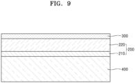
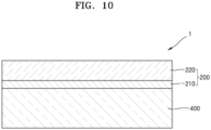
- FIGS. 1 to 10 are diagrams illustrating a method of manufacturing an electronic device (hereinafter, referred to as “electronic device manufacturing method”), according to an embodiment.
- the electronic device manufacturing method includes forming a stack structure 10 by placing a layer 200 (hereinafter, referred to as "to-be-peeled layer”) to be peeled off on a substrate 100, applying thermal shock to the stack structure 10, detaching the to-be-peeled layer 200 from the substrate 100, and transferring the detached to-be-peeled layer 200 to a transfer target 400.
- a layer 200 hereinafter, referred to as "to-be-peeled layer”
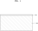
- the substrate 100 is prepared.
- the material of the substrate 100 is not particularly limited, and a generally used silicon substrate may be used as the substrate 100.
- the substrate 100 may include an opaque material. That is, in the electronic device manufacturing method according to an embodiment, a general-purpose substrate may be used as it is, and thus its utilization is high.
- the substrate 100 may include a silicon substrate or a glass substrate.
- a thin film 210 is placed on the substrate 100.
- the thin film 210 is in direct contact with the substrate 100 and is interposed between the substrate 100 and a functional layer 220.
- the thickness of the thin film 210 is not particularly limited, as described later, the thickness of the thin film 210 may be several nm to several hundred nm in order for the thin film 210 to be easily peeled off according to a difference in the coefficient of thermal expansion between the substrate 100 and the thin film 210 when a thermal shock is applied to the stack structure 10.
- the thickness of the thin film 210 may be relatively small so as to implement a flexible electronic device 1.
- the thin film 210 may have a high thermal expansion coefficient and includes metal.
- the thin film 210 may include any one of gold (Au), silver (Ag), and copper (Cu).
- a method of placing the thin film 210 on the substrate 100 is not particularly limited, and a conventional deposition method may be applied.
- a physical vapor deposition (PVD) method such as sputtering deposition or E-beam evaporation may be applied.
- the functional layer 220 is placed on the thin film 210.
- the functional layer 220 may be an electronic element coated with a protective layer.
- the protective layer may be an insulator that protects the electronic element from a physical shock and a sudden temperature change.
- the protective layer may include a polymer such as polyimide.
- the functional layer 220 may be placed on the thin film 210 in the following manner. First, a polymer is coated as a protective layer on the thin film 210 placed on the substrate 100. Next, a metal is deposited on the polymer and patterned. Then, a polymer is again coated to cover a metal part. However, it is not necessary to cover the metal part, and a next process may be performed in an exposed state.
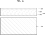
- the to-be-peeled layer 200 is peeled off from the substrate 100 by a peeling process and finally placed on the transfer target 400.
- the substrate 100 and the to-be-peeled layer 200 form the stack structure 10.
- an electronic device of nanometers to meters may be manufactured without distortion and deformation of a shape. Therefore, the sizes and shapes of the thin film 210 and the functional layer 220 are not particularly limited, and the thin film 210 and the functional layer 220 having various shapes and patterns may be used. In addition, the thin film 210 and the functional layer 220 may have shapes corresponding to each other, or the thin film 210 may have a larger area than the functional layer 220.
- the substrate 100 and the thin film 210 may have different thermal expansion coefficients.
- the thermal expansion coefficient of the thin film 210 may be greater than the thermal expansion coefficient of the substrate 100 so that, by a thermal shock, tensile stress acts on the substrate 100 and compressive stress acts on the thin film 210.
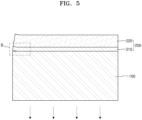
- a thermal shock is applied to the stack structure 10.
- the thermal shock causes a sudden temperature change in an object and causes a physical change in the object.
- the thermal shock is given by heating the stack structure 10 and then immediately cooling the stack structure 10.
- the stack structure 10 is heated.
- the arrow shown in FIG. 3 shows a state in which heat is supplied to the stack structure 10 from the outside.
- a method of heating the stack structure 10 is not specifically limited.
- the stack structure 10 may be placed in a heating chamber or an oven, and then the stack structure 10 may be heated as a whole, the interface between the substrate 100 and the thin film 210 may be selectively heated, or a lower portion of the substrate 100 may be selectively heated using a hot plate or the like.
- a hot plate may be arranged below the substrate 100 as a heating portion to heat the stack structure 10. When the stack structure 10 is heated, thermal stress is generated in the substrate 100 and the thin film 210.
- FIG. 4 which is an enlarged view of an area A of FIG. 3A
- the substrate 100 expands to thereby generate tensile stress therein.
- the thermal expansion coefficient of the thin film 210 is greater than the thermal expansion coefficient of the substrate 100 as described above, the thin film 210 has an expansion ratio greater than that of the substrate 100.
- the thin film 210 is in a state where the shape thereof is fixed by the substrate 100, the expansion of the thin film 210 is restricted, and thus compressive stress is generated inside the thin film 210. Therefore, as indicated by the arrow in FIG.
- thermal stresses in opposite directions occur in an upper portion of the substrate 100 and a lower portion of the thin film 210. Accordingly, shear stress is generated at the interface between the substrate 100 and the thin film 210 in a direction parallel to the interface, thereby weakening a bonding force between the substrate 100 and the thin film 210.
- the heating process is performed until the temperature of the substrate 100 reaches from 100 °C to 400 °C.
- the temperature of the substrate 100 is less than 100 °C, thermal stress is not sufficiently generated in the substrate 100 and the thin film 210, and thus the thin film 210 may not be peeled off from the substrate 100.
- the temperature of the substrate 100 exceeds 400 °C, the functional layer 220 may be damaged.
- the time required for the heating process depends on the materials and sizes of the substrate 100 and the thin film 210, the characteristics of the heating portion, and the like, and is not particularly limited. For example, it may take about 10 minutes to heat the substrate 100 to 400 °C by using a hot plate as the heating portion.
- the stack structure 10 is cooled.
- the arrow shown in FIG. 5 shows a state in which heat is released from the stack structure 10 to the outside.
- a cooling process is carried out immediately after the heating operation is completed, in order to apply a thermal shock to the stack structure 10.
- the stack structure 10 may be cooled as a whole, the interface between the substrate 100 and the thin film 210 may be selectively cooled, or a lower portion of the substrate 100 may be selectively cooled by using a cooling portion.
- the cooling portion may be attached to the lower portion of the substrate 100.
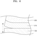
- FIG. 6 which is an enlarged view of an area B of FIG. 5
- the substrate 100 contracts as the temperature thereof drops, and compressive stress is generated in the substrate 100.
- the thermal expansion coefficient of the thin film 210 is greater than the thermal expansion coefficient of the substrate 100 as described above, the thin film 210 has a shrinkage ratio greater than that of the substrate 100.
- the thin film 210 is in a state where the shape thereof is fixed by the substrate 100, the shrinkage of the thin film 210 is restricted, and thus tensile stress is generated inside the thin film 210.
- thermal stress is generated in the stack structure 10 in a direction opposite to that of the thermal stress generated in the heating process. Accordingly, in a state in which a bonding force between the substrate 100 and the thin film 210 is weakened during the heating process, shear stress is generated at the interface between the substrate 100 and the thin film 210 while the thermal stress acts in the opposite direction. As a result, fine peeling occurs from the lengthwise end of the thin film 210, and the thin film 210 is peeled off from the substrate 100. That is, the to-be-peeled layer 200 is peeled off from the substrate 100.
- the cooling portion is not particularly limited. However, in order to quickly cool the heated stack structure 10 and apply thermal shock thereto, a cooling plate including a material having high thermal conductivity may be attached to a lower portion of the substrate 100 to perform cooling. Specifically, an aluminum plate may be used as the cooling plate.
- the time required for the cooling process depends on the materials and sizes of the substrate 100 and the thin film 210 and the characteristics of the cooling portion, and is not particularly limited. However, the time required for the cooling process may be relatively short in order to apply thermal shock to the stack structure 10, and the thin film 210 is easily peeled off from the substrate 100 by cooling the substrate 100 to room temperature within 1 minute.
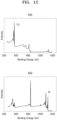
- FIG. 13 is a diagram for comparing the electronic device manufacturing method according to the embodiment and a conventional electronic device manufacturing method.
- the substrate has to include a light-transmitting material that may transmit the laser and it is expensive to construct laser equipment.
- the interface between the substrate and a to-be-peeled layer is heated to a very high temperature, deformation due to high heat is inevitable.
- the laser has to be concentrated in a certain area, it is not suitable for manufacturing a large-area electronic element.
- the electronic device manufacturing method only a time required for cooling the substrate 100 after heating the substrate 100 to a predetermined temperature is required.
- a to-be-peeled layer 200 having a large area may also be peeled off quickly, and thus there is no restriction on the sizes of the thin film 210 and the functional layer 220, and the time required for the electronic device manufacturing process may be shortened.
- the peeling process is performed within a temperature range where deformation caused by heat does not occur, deformation does not occur in the substrate 100 or the to-be-peeled layer 200.
- the peeling process is performed in a state in which the thin film 210 and the functional layer 220 are formed on the substrate 100, and there is no need to additionally form a separate layer (e.g., hydrogen ion implantation layer).
- a separate layer e.g., hydrogen ion implantation layer.
- the process of manufacturing the electronic device 1 is very simple and the time and cost required for the process may be drastically reduced.
- a thin film 210 having an extremely small thickness of several nm may be used to implement a very flexible electronic device 1.
Landscapes
- Chemical & Material Sciences (AREA)
- Organic Chemistry (AREA)
- Engineering & Computer Science (AREA)
- Manufacturing & Machinery (AREA)
- Thin Film Transistor (AREA)
- Laminated Bodies (AREA)
- Manufacturing Of Printed Wiring (AREA)
- Liquid Crystal (AREA)
- Physics & Mathematics (AREA)
- Optics & Photonics (AREA)
Claims (5)
- Procédé de fabrication d'un dispositif électronique, le procédé comprenant :la formation d'une structure empilée en plaçant sur un substrat une couche destinée à être décollée, dans lequel la couche destinée à être décollée comprend un film mince et une couche fonctionnelle, et dans lequel le film mince est placé sur le substrat et la couche fonctionnelle est placée sur le film mince ;l'application d'un choc thermique sur la structure empilée, dans lequel l'application du choc thermique comprend le refroidissement du substrat jusqu'à ce qu'une température du substrat atteigne la température ambiante en 1 minute après le chauffage du substrat jusqu'à ce qu'une température du substrat atteigne une température comprise entre 100 °C et 400 °C, et le fait de provoquer une variation soudaine de la température dans la structure empilée en mettant en oeuvre le refroidissement immédiatement après que le chauffage est terminé ;le détachement de la couche destinée à être décollée à partir du substrat ; etle transfert de la couche destinée à être décollée détachée sur un substrat cible, etdans lequel le film mince comprend un métal présentant un coefficient de dilatation thermique supérieur à un coefficient de dilatation thermique du substrat, etdans lequel l'application du choc thermique comprend la génération d'une contrainte de cisaillement au niveau d'une interface entre le substrat et le film mince afin de retirer par décollement le film mince à partir du substrat.
- Procédé selon la revendication 1, dans lequel l'application du choc thermique comprend la génération de contraintes thermiques dans des directions opposées dans le substrat et dans la couche destinée à être décollée.
- Procédé selon la revendication 1, dans lequel la couche fonctionnelle comprend :une couche de protection en contact avec le film mince ; etun élément électronique agencé sur la couche de protection.
- Procédé selon la revendication 1, dans lequel le détachement de la couche destinée à être décollée comprend la liaison d'une couche de transfert sur la couche destinée à être décollée et le détachement de la couche destinée à être décollée et de la couche de transfert liées l'une à l'autre à partir du substrat.
- Procédé selon la revendication 4, dans lequel la couche de transfert comprend un quelconque ruban parmi un ruban en polydiméthylsiloxane, soit PDMS, à décollement thermique et un ruban soluble à l'eau.
Applications Claiming Priority (1)
| Application Number | Priority Date | Filing Date | Title |
|---|---|---|---|
| KR1020190116259A KR102271268B1 (ko) | 2019-09-20 | 2019-09-20 | 전자장치 제조방법 |
Publications (2)
| Publication Number | Publication Date |
|---|---|
| EP3796406A1 EP3796406A1 (fr) | 2021-03-24 |
| EP3796406B1 true EP3796406B1 (fr) | 2025-01-15 |
Family
ID=68502868
Family Applications (1)
| Application Number | Title | Priority Date | Filing Date |
|---|---|---|---|
| EP19207642.0A Active EP3796406B1 (fr) | 2019-09-20 | 2019-11-07 | Procédé de fabrication d'un dispositif piézoélectrique |
Country Status (4)
| Country | Link |
|---|---|
| US (1) | US11367647B2 (fr) |
| EP (1) | EP3796406B1 (fr) |
| JP (1) | JP6951697B2 (fr) |
| KR (1) | KR102271268B1 (fr) |
Families Citing this family (2)
| Publication number | Priority date | Publication date | Assignee | Title |
|---|---|---|---|---|
| FI129855B (en) * | 2019-10-08 | 2022-09-30 | Jani Oksanen | METHOD AND STRUCTURE FOR MANUFACTURING THIN FILMS |
| JP2026050059A (ja) * | 2024-09-09 | 2026-03-19 | 東レエンジニアリング株式会社 | 素子転写方法および素子転写装置 |
Citations (1)
| Publication number | Priority date | Publication date | Assignee | Title |
|---|---|---|---|---|
| JP2008177182A (ja) * | 2007-01-16 | 2008-07-31 | Seiko Epson Corp | 薄膜デバイスの製造方法 |
Family Cites Families (17)
| Publication number | Priority date | Publication date | Assignee | Title |
|---|---|---|---|---|
| FR2748851B1 (fr) | 1996-05-15 | 1998-08-07 | Commissariat Energie Atomique | Procede de realisation d'une couche mince de materiau semiconducteur |
| KR100481994B1 (ko) | 1996-08-27 | 2005-12-01 | 세이코 엡슨 가부시키가이샤 | 박리방법,박막디바이스의전사방법,및그것을이용하여제조되는박막디바이스,박막집적회로장치및액정표시장치 |
| JP4035862B2 (ja) * | 1997-07-11 | 2008-01-23 | ソニー株式会社 | 半導体基板の製造方法 |
| JP3755333B2 (ja) | 1999-04-09 | 2006-03-15 | 松下電器産業株式会社 | 微細パターンの製造方法及びそれを用いたプリント配線板 |
| JP2001291728A (ja) * | 2000-04-07 | 2001-10-19 | Ind Technol Res Inst | ポリアミド膜工程を用いたパッケージ方法 |
| JP2002171009A (ja) | 2000-12-04 | 2002-06-14 | Canon Inc | 膜の転写方法 |
| JP4127463B2 (ja) | 2001-02-14 | 2008-07-30 | 豊田合成株式会社 | Iii族窒化物系化合物半導体の結晶成長方法及びiii族窒化物系化合物半導体発光素子の製造方法 |
| JP2006049800A (ja) | 2004-03-10 | 2006-02-16 | Seiko Epson Corp | 薄膜デバイスの供給体、薄膜デバイスの供給体の製造方法、転写方法、半導体装置の製造方法及び電子機器 |
| KR101254277B1 (ko) | 2004-07-30 | 2013-04-15 | 가부시키가이샤 한도오따이 에네루기 켄큐쇼 | 라미네이팅 시스템, ic 시트, ic 시트 두루마리, 및ic 칩의 제조방법 |
| JP5064693B2 (ja) | 2006-02-13 | 2012-10-31 | 信越化学工業株式会社 | Soi基板の製造方法 |
| JP2007220782A (ja) | 2006-02-15 | 2007-08-30 | Shin Etsu Chem Co Ltd | Soi基板およびsoi基板の製造方法 |
| JP5041714B2 (ja) | 2006-03-13 | 2012-10-03 | 信越化学工業株式会社 | マイクロチップ及びマイクロチップ製造用soi基板 |
| JP5580155B2 (ja) | 2010-09-27 | 2014-08-27 | スタンレー電気株式会社 | タッチパネル入力装置の製造方法 |
| KR20130126062A (ko) * | 2012-05-10 | 2013-11-20 | 한국과학기술원 | 수용해성 접착제를 이용한 플렉서블 전자소자 제조방법 및 이에 의하여 제조된 플렉서블 전자소자 |
| JP2014120664A (ja) | 2012-12-18 | 2014-06-30 | Dainippon Screen Mfg Co Ltd | 剥離補助方法および剥離補助装置 |
| WO2015073089A1 (fr) | 2013-08-26 | 2015-05-21 | The Regents Of The University Of Michigan | Enlèvement de film mince via une combinaison de soulèvement et d'enlèvement épitaxial |
| KR102013283B1 (ko) * | 2017-12-05 | 2019-08-22 | 재단법인 오송첨단의료산업진흥재단 | 열팽창 계수를 이용한 박막전극 분리 방법 |
-
2019
- 2019-09-20 KR KR1020190116259A patent/KR102271268B1/ko active Active
- 2019-11-06 US US16/675,559 patent/US11367647B2/en active Active
- 2019-11-07 EP EP19207642.0A patent/EP3796406B1/fr active Active
- 2019-11-08 JP JP2019202822A patent/JP6951697B2/ja active Active
Patent Citations (1)
| Publication number | Priority date | Publication date | Assignee | Title |
|---|---|---|---|---|
| JP2008177182A (ja) * | 2007-01-16 | 2008-07-31 | Seiko Epson Corp | 薄膜デバイスの製造方法 |
Also Published As
| Publication number | Publication date |
|---|---|
| KR102271268B1 (ko) | 2021-06-30 |
| JP6951697B2 (ja) | 2021-10-20 |
| EP3796406A1 (fr) | 2021-03-24 |
| JP2021049768A (ja) | 2021-04-01 |
| US11367647B2 (en) | 2022-06-21 |
| US20210090932A1 (en) | 2021-03-25 |
| KR20210034376A (ko) | 2021-03-30 |
Similar Documents
| Publication | Publication Date | Title |
|---|---|---|
| TWI239224B (en) | COF flexible printed wiring board and method of producing the wiring board | |
| CN110165024B (zh) | 微型元件转移方法 | |
| EP2088622A2 (fr) | Procédé de formation d'un dispositif électronique sur un substrat métallique flexible et dispositif résultant | |
| US10930528B2 (en) | Method for transferring micro device | |
| EP3796406B1 (fr) | Procédé de fabrication d'un dispositif piézoélectrique | |
| KR20140103515A (ko) | 전사 인쇄용 스탬프 구조체 및 그 제조 방법과, 스탬프 구조체를 이용한 전사 인쇄 방법 | |
| CN108735919B (zh) | 将薄膜图案化的方法、显示器件及其制备方法 | |
| KR101923772B1 (ko) | 2차원 나노박막을 전사시키는 방법 | |
| US12136569B2 (en) | Semiconductor device manufacturing method and semiconductor device manufacturing system | |
| US10937674B2 (en) | Method for transferring micro device | |
| CN112606583A (zh) | 微图形结构转印方法及微图形结构基板 | |
| JP4186502B2 (ja) | 薄膜デバイスの製造方法、薄膜デバイスおよび表示装置 | |
| US10395954B2 (en) | Method and device for coating a product substrate | |
| TWI381433B (zh) | 結合ic整合基板與載板之結構及其製造方法與電子裝置之製造方法 | |
| US12214580B2 (en) | Method for transferring a layer to a substrate | |
| TW202040833A (zh) | 用於轉移微型元件的方法 | |
| TW202116648A (zh) | 取料裝置 | |
| TWI695416B (zh) | 用於轉移微型元件的方法 | |
| CN113078054B (zh) | 一种电极层的制备方法及半导体结构 | |
| JP2008114448A (ja) | 転写基板とそれを用いた転写方法 | |
| US7144791B2 (en) | Lamination through a mask | |
| CN117174791A (zh) | 微元件转移方法 | |
| CN100375236C (zh) | 形成可分离界面的方法及使用此方法制作微机电薄膜 | |
| TW201935625A (zh) | 用於呈卷形式的電子封裝和其它應用的單分基板 | |
| CN107227457A (zh) | 具有溅镀式无机复合薄膜的附载体铜箔及其制备方法 |
Legal Events
| Date | Code | Title | Description |
|---|---|---|---|
| PUAI | Public reference made under article 153(3) epc to a published international application that has entered the european phase |
Free format text: ORIGINAL CODE: 0009012 |
|
| STAA | Information on the status of an ep patent application or granted ep patent |
Free format text: STATUS: REQUEST FOR EXAMINATION WAS MADE |
|
| 17P | Request for examination filed |
Effective date: 20191107 |
|
| AK | Designated contracting states |
Kind code of ref document: A1 Designated state(s): AL AT BE BG CH CY CZ DE DK EE ES FI FR GB GR HR HU IE IS IT LI LT LU LV MC MK MT NL NO PL PT RO RS SE SI SK SM TR |
|
| AX | Request for extension of the european patent |
Extension state: BA ME |
|
| STAA | Information on the status of an ep patent application or granted ep patent |
Free format text: STATUS: EXAMINATION IS IN PROGRESS |
|
| 17Q | First examination report despatched |
Effective date: 20240514 |
|
| REG | Reference to a national code |
Ref country code: DE Ref legal event code: R079 Free format text: PREVIOUS MAIN CLASS: H01L0051000000 Ipc: H10K0071800000 Ref document number: 602019064821 Country of ref document: DE |
|
| GRAP | Despatch of communication of intention to grant a patent |
Free format text: ORIGINAL CODE: EPIDOSNIGR1 |
|
| STAA | Information on the status of an ep patent application or granted ep patent |
Free format text: STATUS: GRANT OF PATENT IS INTENDED |
|
| RIC1 | Information provided on ipc code assigned before grant |
Ipc: B32B 7/06 20190101ALI20240926BHEP Ipc: H10K 71/80 20230101AFI20240926BHEP |
|
| INTG | Intention to grant announced |
Effective date: 20241023 |
|
| RIN1 | Information on inventor provided before grant (corrected) |
Inventor name: HEO, SEUNG KYOUNG Inventor name: RAH, JONG CHEOL Inventor name: KEUM, HO HYUN Inventor name: JANG, KYUNG IN |
|
| GRAS | Grant fee paid |
Free format text: ORIGINAL CODE: EPIDOSNIGR3 |
|
| GRAA | (expected) grant |
Free format text: ORIGINAL CODE: 0009210 |
|
| STAA | Information on the status of an ep patent application or granted ep patent |
Free format text: STATUS: THE PATENT HAS BEEN GRANTED |
|
| AK | Designated contracting states |
Kind code of ref document: B1 Designated state(s): AL AT BE BG CH CY CZ DE DK EE ES FI FR GB GR HR HU IE IS IT LI LT LU LV MC MK MT NL NO PL PT RO RS SE SI SK SM TR |
|
| REG | Reference to a national code |
Ref country code: CH Ref legal event code: EP Ref country code: GB Ref legal event code: FG4D |
|
| REG | Reference to a national code |
Ref country code: DE Ref legal event code: R096 Ref document number: 602019064821 Country of ref document: DE |
|
| REG | Reference to a national code |
Ref country code: IE Ref legal event code: FG4D |
|
| REG | Reference to a national code |
Ref country code: NL Ref legal event code: MP Effective date: 20250115 |
|
| PG25 | Lapsed in a contracting state [announced via postgrant information from national office to epo] |
Ref country code: NL Free format text: LAPSE BECAUSE OF FAILURE TO SUBMIT A TRANSLATION OF THE DESCRIPTION OR TO PAY THE FEE WITHIN THE PRESCRIBED TIME-LIMIT Effective date: 20250115 |
|
| PG25 | Lapsed in a contracting state [announced via postgrant information from national office to epo] |
Ref country code: RS Free format text: LAPSE BECAUSE OF FAILURE TO SUBMIT A TRANSLATION OF THE DESCRIPTION OR TO PAY THE FEE WITHIN THE PRESCRIBED TIME-LIMIT Effective date: 20250415 |
|
| PG25 | Lapsed in a contracting state [announced via postgrant information from national office to epo] |
Ref country code: FI Free format text: LAPSE BECAUSE OF FAILURE TO SUBMIT A TRANSLATION OF THE DESCRIPTION OR TO PAY THE FEE WITHIN THE PRESCRIBED TIME-LIMIT Effective date: 20250115 |
|
| PG25 | Lapsed in a contracting state [announced via postgrant information from national office to epo] |
Ref country code: PL Free format text: LAPSE BECAUSE OF FAILURE TO SUBMIT A TRANSLATION OF THE DESCRIPTION OR TO PAY THE FEE WITHIN THE PRESCRIBED TIME-LIMIT Effective date: 20250115 |
|
| PG25 | Lapsed in a contracting state [announced via postgrant information from national office to epo] |
Ref country code: ES Free format text: LAPSE BECAUSE OF FAILURE TO SUBMIT A TRANSLATION OF THE DESCRIPTION OR TO PAY THE FEE WITHIN THE PRESCRIBED TIME-LIMIT Effective date: 20250115 |
|
| REG | Reference to a national code |
Ref country code: LT Ref legal event code: MG9D |
|
| PG25 | Lapsed in a contracting state [announced via postgrant information from national office to epo] |
Ref country code: NO Free format text: LAPSE BECAUSE OF FAILURE TO SUBMIT A TRANSLATION OF THE DESCRIPTION OR TO PAY THE FEE WITHIN THE PRESCRIBED TIME-LIMIT Effective date: 20250415 Ref country code: IS Free format text: LAPSE BECAUSE OF FAILURE TO SUBMIT A TRANSLATION OF THE DESCRIPTION OR TO PAY THE FEE WITHIN THE PRESCRIBED TIME-LIMIT Effective date: 20250515 |
|
| REG | Reference to a national code |
Ref country code: AT Ref legal event code: MK05 Ref document number: 1760675 Country of ref document: AT Kind code of ref document: T Effective date: 20250115 |
|
| PG25 | Lapsed in a contracting state [announced via postgrant information from national office to epo] |
Ref country code: HR Free format text: LAPSE BECAUSE OF FAILURE TO SUBMIT A TRANSLATION OF THE DESCRIPTION OR TO PAY THE FEE WITHIN THE PRESCRIBED TIME-LIMIT Effective date: 20250115 |
|
| PG25 | Lapsed in a contracting state [announced via postgrant information from national office to epo] |
Ref country code: PT Free format text: LAPSE BECAUSE OF FAILURE TO SUBMIT A TRANSLATION OF THE DESCRIPTION OR TO PAY THE FEE WITHIN THE PRESCRIBED TIME-LIMIT Effective date: 20250515 Ref country code: LV Free format text: LAPSE BECAUSE OF FAILURE TO SUBMIT A TRANSLATION OF THE DESCRIPTION OR TO PAY THE FEE WITHIN THE PRESCRIBED TIME-LIMIT Effective date: 20250115 |
|
| PG25 | Lapsed in a contracting state [announced via postgrant information from national office to epo] |
Ref country code: BG Free format text: LAPSE BECAUSE OF FAILURE TO SUBMIT A TRANSLATION OF THE DESCRIPTION OR TO PAY THE FEE WITHIN THE PRESCRIBED TIME-LIMIT Effective date: 20250115 Ref country code: GR Free format text: LAPSE BECAUSE OF FAILURE TO SUBMIT A TRANSLATION OF THE DESCRIPTION OR TO PAY THE FEE WITHIN THE PRESCRIBED TIME-LIMIT Effective date: 20250416 |
|
| PG25 | Lapsed in a contracting state [announced via postgrant information from national office to epo] |
Ref country code: AT Free format text: LAPSE BECAUSE OF FAILURE TO SUBMIT A TRANSLATION OF THE DESCRIPTION OR TO PAY THE FEE WITHIN THE PRESCRIBED TIME-LIMIT Effective date: 20250115 |
|
| PG25 | Lapsed in a contracting state [announced via postgrant information from national office to epo] |
Ref country code: SE Free format text: LAPSE BECAUSE OF FAILURE TO SUBMIT A TRANSLATION OF THE DESCRIPTION OR TO PAY THE FEE WITHIN THE PRESCRIBED TIME-LIMIT Effective date: 20250115 |
|
| PG25 | Lapsed in a contracting state [announced via postgrant information from national office to epo] |
Ref country code: SM Free format text: LAPSE BECAUSE OF FAILURE TO SUBMIT A TRANSLATION OF THE DESCRIPTION OR TO PAY THE FEE WITHIN THE PRESCRIBED TIME-LIMIT Effective date: 20250115 |
|
| PG25 | Lapsed in a contracting state [announced via postgrant information from national office to epo] |
Ref country code: DK Free format text: LAPSE BECAUSE OF FAILURE TO SUBMIT A TRANSLATION OF THE DESCRIPTION OR TO PAY THE FEE WITHIN THE PRESCRIBED TIME-LIMIT Effective date: 20250115 |
|
| PG25 | Lapsed in a contracting state [announced via postgrant information from national office to epo] |
Ref country code: IT Free format text: LAPSE BECAUSE OF FAILURE TO SUBMIT A TRANSLATION OF THE DESCRIPTION OR TO PAY THE FEE WITHIN THE PRESCRIBED TIME-LIMIT Effective date: 20250115 |
|
| REG | Reference to a national code |
Ref country code: DE Ref legal event code: R097 Ref document number: 602019064821 Country of ref document: DE |
|
| PGFP | Annual fee paid to national office [announced via postgrant information from national office to epo] |
Ref country code: FR Payment date: 20250925 Year of fee payment: 7 |
|
| PG25 | Lapsed in a contracting state [announced via postgrant information from national office to epo] |
Ref country code: CZ Free format text: LAPSE BECAUSE OF FAILURE TO SUBMIT A TRANSLATION OF THE DESCRIPTION OR TO PAY THE FEE WITHIN THE PRESCRIBED TIME-LIMIT Effective date: 20250115 Ref country code: EE Free format text: LAPSE BECAUSE OF FAILURE TO SUBMIT A TRANSLATION OF THE DESCRIPTION OR TO PAY THE FEE WITHIN THE PRESCRIBED TIME-LIMIT Effective date: 20250115 |
|
| PG25 | Lapsed in a contracting state [announced via postgrant information from national office to epo] |
Ref country code: RO Free format text: LAPSE BECAUSE OF FAILURE TO SUBMIT A TRANSLATION OF THE DESCRIPTION OR TO PAY THE FEE WITHIN THE PRESCRIBED TIME-LIMIT Effective date: 20250115 |
|
| PG25 | Lapsed in a contracting state [announced via postgrant information from national office to epo] |
Ref country code: SK Free format text: LAPSE BECAUSE OF FAILURE TO SUBMIT A TRANSLATION OF THE DESCRIPTION OR TO PAY THE FEE WITHIN THE PRESCRIBED TIME-LIMIT Effective date: 20250115 |
|
| PLBE | No opposition filed within time limit |
Free format text: ORIGINAL CODE: 0009261 |
|
| STAA | Information on the status of an ep patent application or granted ep patent |
Free format text: STATUS: NO OPPOSITION FILED WITHIN TIME LIMIT |
|
| 26N | No opposition filed |
Effective date: 20251016 |
|
| PGFP | Annual fee paid to national office [announced via postgrant information from national office to epo] |
Ref country code: DE Payment date: 20250922 Year of fee payment: 7 |