EP3796408A1 - Structure de pérovskite multicouches et son procédé de fabrication - Google Patents
Structure de pérovskite multicouches et son procédé de fabrication Download PDFInfo
- Publication number
- EP3796408A1 EP3796408A1 EP20179571.3A EP20179571A EP3796408A1 EP 3796408 A1 EP3796408 A1 EP 3796408A1 EP 20179571 A EP20179571 A EP 20179571A EP 3796408 A1 EP3796408 A1 EP 3796408A1
- Authority
- EP
- European Patent Office
- Prior art keywords
- layer
- metal
- perovskite
- multilayered structure
- substrate
- Prior art date
- Legal status (The legal status is an assumption and is not a legal conclusion. Google has not performed a legal analysis and makes no representation as to the accuracy of the status listed.)
- Granted
Links
Images


Classifications
-
- H—ELECTRICITY
- H10—SEMICONDUCTOR DEVICES; ELECTRIC SOLID-STATE DEVICES NOT OTHERWISE PROVIDED FOR
- H10K—ORGANIC ELECTRIC SOLID-STATE DEVICES
- H10K71/00—Manufacture or treatment specially adapted for the organic devices covered by this subclass
- H10K71/10—Deposition of organic active material
- H10K71/16—Deposition of organic active material using physical vapour deposition [PVD], e.g. vacuum deposition or sputtering
- H10K71/164—Deposition of organic active material using physical vapour deposition [PVD], e.g. vacuum deposition or sputtering using vacuum deposition
-
- H—ELECTRICITY
- H10—SEMICONDUCTOR DEVICES; ELECTRIC SOLID-STATE DEVICES NOT OTHERWISE PROVIDED FOR
- H10K—ORGANIC ELECTRIC SOLID-STATE DEVICES
- H10K30/00—Organic devices sensitive to infrared radiation, light, electromagnetic radiation of shorter wavelength or corpuscular radiation
- H10K30/30—Organic devices sensitive to infrared radiation, light, electromagnetic radiation of shorter wavelength or corpuscular radiation comprising bulk heterojunctions, e.g. interpenetrating networks of donor and acceptor material domains
-
- H—ELECTRICITY
- H10—SEMICONDUCTOR DEVICES; ELECTRIC SOLID-STATE DEVICES NOT OTHERWISE PROVIDED FOR
- H10K—ORGANIC ELECTRIC SOLID-STATE DEVICES
- H10K30/00—Organic devices sensitive to infrared radiation, light, electromagnetic radiation of shorter wavelength or corpuscular radiation
- H10K30/40—Organic devices sensitive to infrared radiation, light, electromagnetic radiation of shorter wavelength or corpuscular radiation comprising a p-i-n structure, e.g. having a perovskite absorber between p-type and n-type charge transport layers
-
- H—ELECTRICITY
- H10—SEMICONDUCTOR DEVICES; ELECTRIC SOLID-STATE DEVICES NOT OTHERWISE PROVIDED FOR
- H10K—ORGANIC ELECTRIC SOLID-STATE DEVICES
- H10K71/00—Manufacture or treatment specially adapted for the organic devices covered by this subclass
-
- H—ELECTRICITY
- H10—SEMICONDUCTOR DEVICES; ELECTRIC SOLID-STATE DEVICES NOT OTHERWISE PROVIDED FOR
- H10K—ORGANIC ELECTRIC SOLID-STATE DEVICES
- H10K71/00—Manufacture or treatment specially adapted for the organic devices covered by this subclass
- H10K71/10—Deposition of organic active material
- H10K71/12—Deposition of organic active material using liquid deposition, e.g. spin coating
-
- H—ELECTRICITY
- H10—SEMICONDUCTOR DEVICES; ELECTRIC SOLID-STATE DEVICES NOT OTHERWISE PROVIDED FOR
- H10K—ORGANIC ELECTRIC SOLID-STATE DEVICES
- H10K71/00—Manufacture or treatment specially adapted for the organic devices covered by this subclass
- H10K71/10—Deposition of organic active material
- H10K71/16—Deposition of organic active material using physical vapour deposition [PVD], e.g. vacuum deposition or sputtering
-
- H—ELECTRICITY
- H10—SEMICONDUCTOR DEVICES; ELECTRIC SOLID-STATE DEVICES NOT OTHERWISE PROVIDED FOR
- H10K—ORGANIC ELECTRIC SOLID-STATE DEVICES
- H10K85/00—Organic materials used in the body or electrodes of devices covered by this subclass
- H10K85/30—Coordination compounds
-
- H—ELECTRICITY
- H10—SEMICONDUCTOR DEVICES; ELECTRIC SOLID-STATE DEVICES NOT OTHERWISE PROVIDED FOR
- H10K—ORGANIC ELECTRIC SOLID-STATE DEVICES
- H10K85/00—Organic materials used in the body or electrodes of devices covered by this subclass
- H10K85/50—Organic perovskites; Hybrid organic-inorganic perovskites [HOIP], e.g. CH3NH3PbI3
-
- H—ELECTRICITY
- H10—SEMICONDUCTOR DEVICES; ELECTRIC SOLID-STATE DEVICES NOT OTHERWISE PROVIDED FOR
- H10K—ORGANIC ELECTRIC SOLID-STATE DEVICES
- H10K2101/00—Properties of the organic materials covered by group H10K85/00
- H10K2101/80—Composition varying spatially, e.g. having a spatial gradient
-
- H—ELECTRICITY
- H10—SEMICONDUCTOR DEVICES; ELECTRIC SOLID-STATE DEVICES NOT OTHERWISE PROVIDED FOR
- H10K—ORGANIC ELECTRIC SOLID-STATE DEVICES
- H10K30/00—Organic devices sensitive to infrared radiation, light, electromagnetic radiation of shorter wavelength or corpuscular radiation
- H10K30/50—Photovoltaic [PV] devices
-
- Y—GENERAL TAGGING OF NEW TECHNOLOGICAL DEVELOPMENTS; GENERAL TAGGING OF CROSS-SECTIONAL TECHNOLOGIES SPANNING OVER SEVERAL SECTIONS OF THE IPC; TECHNICAL SUBJECTS COVERED BY FORMER USPC CROSS-REFERENCE ART COLLECTIONS [XRACs] AND DIGESTS
- Y02—TECHNOLOGIES OR APPLICATIONS FOR MITIGATION OR ADAPTATION AGAINST CLIMATE CHANGE
- Y02E—REDUCTION OF GREENHOUSE GAS [GHG] EMISSIONS, RELATED TO ENERGY GENERATION, TRANSMISSION OR DISTRIBUTION
- Y02E10/00—Energy generation through renewable energy sources
- Y02E10/50—Photovoltaic [PV] energy
- Y02E10/549—Organic PV cells
-
- Y—GENERAL TAGGING OF NEW TECHNOLOGICAL DEVELOPMENTS; GENERAL TAGGING OF CROSS-SECTIONAL TECHNOLOGIES SPANNING OVER SEVERAL SECTIONS OF THE IPC; TECHNICAL SUBJECTS COVERED BY FORMER USPC CROSS-REFERENCE ART COLLECTIONS [XRACs] AND DIGESTS
- Y02—TECHNOLOGIES OR APPLICATIONS FOR MITIGATION OR ADAPTATION AGAINST CLIMATE CHANGE
- Y02P—CLIMATE CHANGE MITIGATION TECHNOLOGIES IN THE PRODUCTION OR PROCESSING OF GOODS
- Y02P70/00—Climate change mitigation technologies in the production process for final industrial or consumer products
- Y02P70/50—Manufacturing or production processes characterised by the final manufactured product
-
- Y—GENERAL TAGGING OF NEW TECHNOLOGICAL DEVELOPMENTS; GENERAL TAGGING OF CROSS-SECTIONAL TECHNOLOGIES SPANNING OVER SEVERAL SECTIONS OF THE IPC; TECHNICAL SUBJECTS COVERED BY FORMER USPC CROSS-REFERENCE ART COLLECTIONS [XRACs] AND DIGESTS
- Y10—TECHNICAL SUBJECTS COVERED BY FORMER USPC
- Y10S—TECHNICAL SUBJECTS COVERED BY FORMER USPC CROSS-REFERENCE ART COLLECTIONS [XRACs] AND DIGESTS
- Y10S977/00—Nanotechnology
- Y10S977/70—Nanostructure
- Y10S977/811—Of specified metal oxide composition, e.g. conducting or semiconducting compositions such as ITO, ZnOx
- Y10S977/812—Perovskites and superconducting composition, e.g. BaxSr1-xTiO3
Definitions
- the present disclosure relates to a perovskite multilayered structure and a manufacturing method thereof, and more particularly, to a perovskite multilayered structure having a graded-bandgap and a manufacturing method thereof.
- Perovskites refers to materials or compounds having a perovskite crystal structure such as the crystal structure of ABX 3 , for example.
- Inorganic metal oxide perovskites have inorganic metal oxides.
- metal cations such as Ti, Sr, Ca, Cs, Ba, Y, Gd, La, Fe, and Mn (e.g., alkali metal, alkaline earth metal, transition metal and lanthanum group, etc.) having different sizes may be positioned at A site and B site, while oxygen anions may be positioned at X site.
- Halide perovskites are different in composition from inorganic metal oxide perovskites in that organic compounds are positioned at the A site and halogen anions are positioned at the X site.
- perovskites As the crystal structure is filled with various elements, the physical properties of perovskites may vary. Inorganic metal oxide perovskites exhibit characteristics such as superconductivity, ferroelectricity, high magnetoresistance, which can be used for sensors, fuel cells, memory devices, and the like.
- halide perovskites can be obtained using inexpensive raw materials and solution processes. Also, halide perovskites are highly compatible with existing semiconductor processes while having excellent optical and electrical characteristics. Thus, halide perovskites are spotlighted as the next generation materials for optoelectronic devices (e.g., solar cells, light emitting diodes, photodetectors, etc.). In the field of solar cells, there are increasing expectations that halide perovskite-based solar cells will replace silicon-based solar cells or be used in tandem with silicon-based solar cells.
- optoelectronic devices e.g., solar cells, light emitting diodes, photodetectors, etc.
- perovskites generally have a single layer structure, there is a considerable limit on the modification or improvement of the physical properties of perovskites.
- a solvent such as dimethylformamide (DMF) or dimethyl sulfoxide (DMSO) used in spin coating process may dissolve perovskites.
- DMF dimethylformamide
- DMSO dimethyl sulfoxide
- DMF or DMSO to be used for forming the second perovskite may dissolve the first perovskite layer. Accordingly, only single-layered perovskites can be formed through the spin coating process, and it is impossible to form multilayered perovskites in a simple and cost-effective manner.
- the present disclosure has been made to overcome the problems mentioned above, and it is an object of the present disclosure to provide a perovskite multilayered structure and a manufacturing method thereof.
- Another object of the present disclosure is to manufacture a perovskite multilayered structure using vapor deposition.
- Yet another object of the present disclosure is to manufacture a perovskite multilayered structure having a graded bandgap by use of vapor deposition.
- a perovskite multilayered structure can be manufactured using vapor deposition.
- a perovskite multilayered structure with a graded bandgap may be formed using vapor deposition.
- the presently disclosed subject matter provides a method of manufacturing a perovskite multilayered structure, comprising: providing a substrate; forming a first perovskite layer on the substrate; forming a metal layer on the first perovskite layer by exposing the substrate to at least one of metal halides, metal oxides, or metal sulfides in a vapor phase; and supplying halogen compounds onto the metal layer to form a second perovskite layer by a reaction between the halogen compounds and at least one of the metal halides, the metal oxides, or the metal sulfides included in the metal layer.
- the halogen compounds are supplied onto the metal layer in a solution phase.
- the halogen compounds are supplied onto the metal layer in a vapor phase.
- the presently disclosed subject matter provides a method of manufacturing a perovskite multilayered structure, comprising: providing a substrate; forming a first perovskite layer on the substrate; supplying halogen compounds in a vapor phase and at least one of metal halides, metal oxides, or metal sulfides in a vapor phase onto the first perovskite layer; and forming a second perovskite layer by a reaction between the halogen compounds and at least one of the metal halides, the metal oxides, or the metal sulfides.
- the second perovskite layer is formed through a dual source vapor deposition process.
- composition of the first perovskite layer and the composition of the second perovskite layer are different from each other.
- the perovskite multilayered structure has a graded bandgap.
- the presently disclosed subject matter provides perovskite multilayered structure, comprising: a first perovskite layer; and a second perovskite layer formed on the first perovskite layer.
- the second perovskite layer is formed by a reaction between a metal layer and halogen compounds.
- the metal layer is formed by depositing at least one of metal halides, metal oxides, or metal sulfides in a vapor phase on the first perovskite layer.
- the presently disclosed subject matter provides a perovskite multilayered structure, comprising: a first perovskite layer; and a second perovskite layer formed on the first perovskite layer.
- the second perovskite layer is formed by a reaction between halogen compounds in a vapor phase and at least one of metal halides, metal oxides, or metal sulfides in a vapor phase.
- composition of the first perovskite layer and the composition of the second perovskite layer are different from each other.
- perovskite or “PE” refers to materials or compounds having a perovskite crystal structure, which may have various perovskite crystal structures in addition to the crystal structure of ABX3.
- the term "optoelectronic device” is used to refer to a device, which can convert light into energy and vice versa.
- the optoelectronic device may include light emitting diode (LED), solar cell, photodetector, X-ray detector, or laser.
- halides refers to materials or compounds containing halogen belonging to group 17 of the periodic table in the form of functional groups, and may include chlorine, bromine, fluorine or iodine compounds, for example.
- halides or “halogen compounds” may be in a solution phase dissolved in a solvent or in a vapor or plasma phase.
- the term “layer” refers to a form of a layer having with a thickness.
- the layer may be porous or non-porous. By “(being) porous,” it means having a porosity.
- the layer may have a bulk form or may be a single crystal thin film.
- vapor phase refers to the vapor phase as well as the plasma phase.
- FIG. 1 is a flowchart showing a method of manufacturing a PE multilayered structure according to an embodiment of the present disclosure.
- a substrate is provided.
- the substrate may be one of a glass substrate, a thin film glass substrate, or a plastic substrate in consideration of the desired properties (e.g., transparency, surface smoothness, water resistance, etc.).
- a substrate may be modified to meet the purpose of the PE multilayered structure formed on the substrate.
- the substrate may be single-layered or multilayered.
- a first electrode may be formed on the substrate.
- the first electrode may be an anode or a cathode.
- the first electrode may be a conductive oxide such as indium-tin oxide (ITO) or indium-zinc oxide (IZO), fluorine-doped tin oxide (FTO).
- the first electrode may include a material selected from the group consisting of silver (Ag), gold (Au), magnesium (Mg), aluminum (Al), platinum (Pt), tungsten (W), copper (Cu), molybdenum (Mo), nickel (Ni), palladium (Pd), chromium (Cr), calcium (Ca), samarium (Sm), lithium (Li), and combinations thereof.
- the first electrode may form on a flexible and transparent material.
- an electron transporting layer (ETL) or a hole transporting layer (HTL) may be formed on the first electrode.
- the electron transporting layer may be a semiconductor including an "n-type material.”
- the "n-type material” means an electron-transporting material.
- the electron-transporting material may be at least one of electron-transporting elements or compounds.
- the electron-transporting electrons or compounds may be undoped or doped with one or more dopant elements.
- the hole transporting layer may be a semiconductor including a "p-type material.”
- the "p-type material” means a hole-transporting material.
- the hole-transporting material may be at least one of hole-transporting elements or compounds.
- the hole-transporting elements or compounds may be undoped or doped with one or more dopant elements.
- the electron transporting layer or the hole transporting layer may be a buffer layer or may include a buffer layer.
- the surface of the electron transporting layer or hole transporting layer may be modified using doping.
- the electron transporting layer or the hole transporting layer may be formed by spin coating, dip coating, inkjet printing, gravure printing, spray coating, bar coating, gravure coating, brush painting, thermal evaporation, sputtering, E-Beam, screen printing, or blade process.
- the electron transporting layer or the hole transporting layer may be coated in a film form or be deposited on the surface of the electrode.
- a first PE layer is formed on the substrate.
- the first PE layer may be formed in direct contact with the substrate.
- the first PE layer may be formed in direct contact with the first electrode.
- the first PE layer may be formed in direct contact with the electron transporting layer or the hole transporting layer.
- the first PE layer may be formed through various processes including vapor deposition process and solution process.
- the first PE layer may be formed using a vapor deposition process.
- the vapor deposition process may include depositing materials onto the surface of a target object (e.g., a substrate) by supplying the materials in a vaporized or plasma phase into a vacuum chamber.
- a target object e.g., a substrate
- metal halides e.g., Pbh
- Pbh metal halides
- an organic halide solution e.g., methylammonium iodide (MAI) solution
- the first PE layer may be formed by depositing the metal halides, which are converted into a vapor phase by heat, on the substrate in a vacuum state, and then applying the organic halide solution onto the substrate that is rotating.
- the first PE layer may be formed by depositing the metal halides, which are converted into a vapor phase by heat, on the substrate in a vacuum state, and then exposing the substrate to the organic halide solution vapor.
- the first PE layer may be formed through coating process using solution.
- the coating process may be selected from the group consisting of spin coating, bar coating, nozzle printing, spray coating, slot die coating, gravure printing, inkjet printing, screen printing, electrohydrodynamic jet printing, electrospray, and combinations thereof.
- adduct complexes are prepared.
- the adduct complexes include a first compound and a second compound which are dissolved in a first solvent.
- the adduct complexes dissolved in the first solvent are applied onto the substrate.
- a second solvent is added and coated on the substrate.
- An anti-solvent is applied on the substrate and the substrate is vacuum-annealed.
- the first compound may be organic halides (e.g., CH 3 NH 3 Br)
- the second compound may be metal halides (e.g.
- the first solvent may be dimethylformamide (DMF) or dimethylsulfoxide (DMSO)
- the second solvent may be diethylether or toluene
- the anti-solvent may be chloroform.
- the anti-solvent means a solvent which does not dissolve perovskite.
- An exemplary anti-solvent may include a non-polar organic solvent.
- a metal layer is formed on the first PE layer using vapor deposition.
- the metal layer may include at least one of metal halides, metal oxides, or metal sulfides.
- the metal halides may have the formula BX2, where B may be a metal cation selected from the group consisting of Pb, Sn, Cu, Ni, Co, Fe, Mn, Cr, Pd, Cd, Yb, Ge, Ca, Sr, Eu and combinations thereof, and X may be a halide anion.
- the metal halides may be PbI 2 or PbBr2, although not limited thereto.
- the metal halides may include a chalcogenide anion in place of, or in addition to at least some of the halide anions.
- the metal oxides may have the formula BO, where B may include a metal cation selected from the group consisting of Pb, Sn, Cu, Ni, Co, Fe, Mn, Cr, Pd, Cd, Yb, Ge, Ca, Sr, Eu and combinations thereof.
- B may include a metal cation selected from the group consisting of Pb, Sn, Cu, Ni, Co, Fe, Mn, Cr, Pd, Cd, Yb, Ge, Ca, Sr, Eu and combinations thereof.
- the metal oxide may be PbO or SnO.
- the metal sulfides may have the formula BS, where B may include a metal cation selected from the group consisting of Pb, Sn, Cu, Ni, Co, Fe, Mn, Cr, Pd, Cd, Yb, Ge, Ca, Sr, Eu and combinations thereof.
- B may include a metal cation selected from the group consisting of Pb, Sn, Cu, Ni, Co, Fe, Mn, Cr, Pd, Cd, Yb, Ge, Ca, Sr, Eu and combinations thereof.
- the metal sulfide may be PbS or SnS.
- metal halides, metal oxides, or metal sulfides which are converted into a vapor phase by heat , may be deposited on the substrate in a vacuum to form a metal layer (that is, metal halide layer, metal oxide layer, or metal sulfide layer). Since the metal halide layer, the metal oxide layer, or the metal sulfide layer is formed through vapor deposition without solvent on the first PE layer, the problem can be solved that the first PE layer is dissolved by the solvent during the formation of a second PE layer.
- a combination of any one or more of metal halides, metal oxides, and metal sulfides, which are converted into a vapor phase by heat, may be deposited on the substrate in a vacuum to form a metal layer. Since the metal layer is formed on the first PE layer through the vapor deposition without solvent, the problem can be solved that the first PE layer is dissolved by the solvent during the formation of a second PE layer.
- halogen compounds are supplied to the substrate to form a second PE layer using a reaction between the halogen compounds and at least one of metal halides, metal oxides, or metal sulfides included in the metal layer and.
- the halogen compounds may be provided on the metal layer in a solution or vapor phase.
- the halogen compounds may have the formula AX, where A may be an organic cation or an alkali metal cation, and X may include a halide anion.
- the halogen compounds may include a chalcogenide anion in place of, or in addition to at least some of the halide anions.
- the organic cation includes a carbon.
- the organic cation may further include other elements, and for example, may further include hydrogen, nitrogen or oxygen.
- the reaction between the metal layer and the halogen compounds may occur by the immersion process, the spin coating process, or the vapor deposition process.
- the reaction may also occur in the processes other than those described herein.
- the second PE layer may be formed by immersing the substrate with the metal layer in a solution containing the halogen compounds, causing a reaction between the halogen compounds and any least one of the metal halides, the metal oxides, or the metal sulfides included in the metal layer.
- the second PE layer may be formed by applying a solvent containing halogen compounds onto a substrate that includes the metal layer.
- the substrate with the metal layer may rotate and be spin-coated, causing a reaction between the halogen compounds and at least one of the metal halides, the metal oxides, or the metal sulfides included in the metal layer.
- the second PE layer may be formed by exposing the substrate including the metal layer to the halogen compound vapor, causing a reaction between the halogen compounds and at least one of the metal halides, the metal oxides, or the metal sulfides included in the metal layer.
- an electron transporting layer or a hole transporting layer may be formed on the second PE layer.
- a second electrode may be formed.
- the second electrode may be an anode or a cathode. The method of forming the electron transporting layer, the hole transporting layer, or the electrode is the same as that described above.
- the solar cell may have a structure in which the first electrode, the electron transporting layer, the first PE layer, the second PE layer, the hole transporting layer, and the second electrode are sequentially stacked.
- the solar cell may have a structure in which the first electrode, the hole transporting layer, the first PE layer, the second PE layer, the electron transporting layer, and the second electrode are sequentially stacked.
- FIG. 2 is a flowchart showing a method of manufacturing a PE multilayered structure according to another embodiment of the present disclosure.
- the substrate is provided, and at S204, the first PE layer is formed. Since the operations at S102 and S104 may be applied to the operations at S202 and S204, respectively, detailed descriptions of S202 and S204 will be omitted.
- the second PE layer is formed on the first PE layer using vapor deposition.
- the thickness of the second PE layer may be controlled through the vapor deposition. For example, the vapor deposition process may continue until the second PE layer reaches a thickness of 10 nm to 100 ⁇ m.
- the process of forming the second PE layer by the vapor deposition may be accomplished by evaporating reactants to produce vapor and exposing the first PE layer to the vapor to form the second PE layer on the first PE layer. Since the second PE layer is formed through the vapor deposition without solvent, the problem can be solved that the first PE layer is dissolved by the solvent during the formation of the second PE layer.
- the vapor deposition may be dual source vapor deposition.
- the vapor exposed on the first PE layer includes compounds produced from two separate sources.
- the dual source vapor deposition equipment may be modified to use three or more sources.
- the reactants may include a first source reactant and a second source reactant.
- the first source reactant may include at least one of the metal halides, the metal oxides, or the metal sulfides.
- the metal halides may have the formula BX2, where B may include a metal cation selected from the group consisting of Pb, Sn, Cu, Ni, Co, Fe, Mn, Cr, Pd, Cd, Yb, Ge, Ca, Sr, Eu and combinations thereof, and X may include a halide anion.
- the metal halides may be PbI 2 or PbBr 2 .
- the metal halides may include a chalcogenide anion in place of, or in addition to at least some of the halide anions.
- the metal oxides may have the formula BO, where B may include a metal cation selected from the group consisting of Pb, Sn, Cu, Ni, Co, Fe, Mn, Cr, Pd, Cd, Yb, Ge, Ca, Sr, Eu and combinations thereof.
- B may include a metal cation selected from the group consisting of Pb, Sn, Cu, Ni, Co, Fe, Mn, Cr, Pd, Cd, Yb, Ge, Ca, Sr, Eu and combinations thereof.
- the metal oxides may be PbO or SnO.
- the metal sulfides may have the formula BS, where B may include a metal cation selected from the group consisting of Pb, Sn, Cu, Ni, Co, Fe, Mn, Cr, Pd, Cd, Yb, Ge, Ca, Sr, Eu and combinations thereof.
- B may include a metal cation selected from the group consisting of Pb, Sn, Cu, Ni, Co, Fe, Mn, Cr, Pd, Cd, Yb, Ge, Ca, Sr, Eu and combinations thereof.
- the metal sulfides may be PbS or SnS.
- the second source reactant may include halogen compounds.
- the halogen compounds may have the formula AX, where A may be an organic cation or an alkali metal cation, and X may be a halide anion.
- the halogen compounds may include a chalcogenide anion in place of, or in addition to at least some of the halide anions.
- the organic cation includes a carbon.
- the organic cation may further include other elements, for example, may further include hydrogen, nitrogen or oxygen.
- the halogen compounds may be organic halides.
- the organic cation of the organic halides may include at least one of methylammonium (MA) or formamidinium (FA).
- the organic halides may be methylammonium chloride, methylammonium bromide, methylammonium iodide, formamidinium chloride, formamidinium bromide, or formamidinium iodide.
- the organic cation may have the formula (R1R2R3R4N) + .
- R1 to R4 may correspond to hydrogen, unsubstituted or substituted C1 to C20 alkyl, or unsubstituted or substituted aryl.
- the organic cation may have the formula (R5NH 3 ) + , where R5 may correspond to hydrogen or substituted or unsubstituted C1 to C20 alkyl.
- the problem can be solved that the first PE layer may be dissolved after forming the first PE layer.
- the first PE layer may be dissolved by a solvent using DMF (N, N-Dimethylformamide), DMSO (Dimethysulfoxide).
- the first PE layer may be prevented from being dissolved by use of the metal layer or by use of the vapor deposition without any solvent.
- the PE multilayered structure may have a graded bandgap, which will further improve the conversion efficiency of the optoelectronic device that includes the PE multilayered structure.
- the graded bandgap may be implemented by varying the halogen compounds included in the first PE layer and the halogen compounds included in the second PE layer as shown in the table below.
- the graded bandgap means that the bandgap of the first PE layer and the bandgap of the second PE layer continuously changes rather than being discrete from each other.
- FIGS. 3 and 4 are XRD graph and SEM image of a PE single layer (MAPbI 3 thin film) formed by the sputtering process according to an embodiment of the present disclosure.
- the PE single layer formed using the sputtering process may be the first PE layer or the second PE layer in the PE multilayered structure.
- a PbI 2 thin film is deposited on the substrate using sputtering process.
- the MAPbI 3 thin film is formed by exposing the PbI 2 thin film to the methylammonium iodide (MAI) in a vapor phase.
- MAI methylammonium iodide
- X-rays are diffracted with respect to the formed MAPbI 3 thin film in X-ray diffraction (XRD) equipment.
- XRD X-ray diffraction
- the Scanning Electron Microscope (SEM) image captured from the cross section of the MAPbI 3 thin film corresponds to FIG. 4 .
- the cross-sectional thickness of the MAPbI 3 thin film was about 500 nm.
- FIGS. 5 and 6 are XRD graph and SEM image of the PE single layer (MAPbBr 3 ) formed by the spin coating process according to another embodiment of the present disclosure.
- the PE single layer formed using the spin coating process may be the first PE layer in the PE multilayered structure.
- adduct complexes are prepared.
- the adduct complexes include a first compound and a second compound which are dissolved in a first solvent.
- the adduct complexes dissolved in the first solvent are applied onto the substrate.
- a second solvent is added and coated on the substrate.
- An anti-solvent is applied on the substrate and the substrate is vacuum-annealed.
- the first compound is CH 3 NH 3 Br and the second compound is PbBr 2 .
- An XRD graph is obtained by measuring the intensity of the diffracted X-rays with respect to the MAPbBr 3 thin film, which corresponds to FIG. 5 .
- the SEM image captured from the cross section of the MAPbBr 3 thin film corresponds to FIG. 6 .
- the cross-sectional thickness of the MAPbI 3 thin film varies depending on the positions, which is about 126 nm, about 180 nm, about 200 nm, and about 400 nm.
- FIGS. 7 and 8 are XRD graph and SEM image of a PE multilayered structure including a first PE layer and a second PE layer manufactured according to an embodiment of the present disclosure.
- the PbI 2 thin film is deposited on the MAPbBr 3 thin film by using the sputtering process.
- the PE multilayered structure is finally manufactured, in which the MAPbBr 3 thin film is the first PE layer or the lower layer and the MAPbI 3 thin film is the second PE layer or the upper layer.
- the flow rate of MAI vapor may be 1 to 200 standard cubic centimeters per minute (sccm, cm 3 /min), and the exposure (reaction) time to MAI vapor may be 1 minute to 10 hours.
- the pressure of the chamber may be 0.1 to 760 Torr, the temperature of the substrate may be 70 to 150 °C, and the temperature of the MAI vapor may be 80 to 300 °C.
- the result of diffracting the X-rays with respect to the PE multilayered structure corresponds to the upper graph among the three XRD graphs shown in the XRD graph of FIG. 7 .
- the middle and lower graphs are provided for reference, which correspond to the XRD graph of MAPbBr 3 shown in FIG. 5 and to the XRD graph of MAPbI 3 shown in FIG. 3 , respectively. It can be seen that the peaks of the XRD graph of MAPbBr 3 (i.e.
- the middle XRD graph and the peaks of the XRD graph of MAPbI 3 correspond to the peaks of the XRD graph of the PE multilayered structure that includes the MAPbBr3 thin film and the MAPbI 3 thin film (i.e., the upper XRD graph).
- MAPbBr3 the lower layer composition
- MAPbI 3 the upper layer composition
- the PE multilayered structure may have a discrete bandgap between the PE layers.
- the thickness of each layer varies depending on the location, the thickness of the first PE layer is about 500 nm, the thickness of the second PE layer is about 490 nm, and the total thickness of the multilayered structure is about 956 nm (see the numerical values in FIG. 8 ).
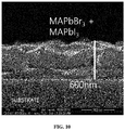
- FIGS. 9 and 10 are XRD graph and SEM image of a PE multilayered structure including a first PE layer and a second PE layer manufactured according to another embodiment of the present disclosure. While the perovskite multilayered structure is prepared according to the same process as that described above with reference to FIGS. 7 and 8 , after depositing the PbI 2 thin film on the MAPbBr 3 thin film using the sputtering process, the time and/or temperature of exposure or reaction to MAI vapor may vary.
- the result of diffracting the X-rays with respect to the PE multilayered structure corresponds to the upper graph among the three XRD graphs shown in the XRD graph of FIG. 9 .
- the middle and lower graphs are provided for reference, which correspond to the XRD graph of MAPbBr 3 shown in FIG. 5 and to the XRD graph of MAPbI 3 shown in FIG. 3 , respectively. It may be seen that the peaks of the XRD graph of MAPbBr 3 (i.e.
- the PE multilayered structure may have a graded bandgap. If necessary, the bandgap of the PE multilayered structure may be discrete or graded, which enables the PE multilayered structure to be used for various purposes.
- the multilayered structure with a graded bandgap has a continuous change of the composition, and therefore, each layer is not divided clearly.
- the total thickness of the multilayer structure is about 600 nm (see the numerical values in FIG. 10 ).
- the PE multilayered structure manufactured by the method described above may be incorporated into an optoelectronic device.
- the optoelectronic device may be a light emitting diode (LED), a solar cell, a photodetector, an X-ray detector, or a laser.
- the PE multilayered structure manufactured by the method described above may be incorporated into a color filter, a photo catalysis, a phototransistor, or a memrister.
- a plurality of layers may be formed by repeating the operations as stated above. Accordingly, a halide PE multilayered structure that has a desired number of layers may be formed. Using such halide PE multilayered structure, an optoelectronic device may absorb light of a wide wavelength range, or an optoelectronic device may emit light of various colors. Further, by use of the PE multilayered structure, it is possible to control the physical properties of PE for color filters, photo catalysts, phototransistors, or memristors.
Landscapes
- Engineering & Computer Science (AREA)
- Chemical & Material Sciences (AREA)
- Manufacturing & Machinery (AREA)
- Materials Engineering (AREA)
- Physics & Mathematics (AREA)
- Electromagnetism (AREA)
- Inorganic Chemistry (AREA)
- Physical Vapour Deposition (AREA)
Applications Claiming Priority (1)
| Application Number | Priority Date | Filing Date | Title |
|---|---|---|---|
| KR1020190115580A KR102227526B1 (ko) | 2019-09-19 | 2019-09-19 | 복층 구조의 페로브스카이트 및 그 제조방법 |
Publications (2)
| Publication Number | Publication Date |
|---|---|
| EP3796408A1 true EP3796408A1 (fr) | 2021-03-24 |
| EP3796408B1 EP3796408B1 (fr) | 2025-09-17 |
Family
ID=71092458
Family Applications (1)
| Application Number | Title | Priority Date | Filing Date |
|---|---|---|---|
| EP20179571.3A Active EP3796408B1 (fr) | 2019-09-19 | 2020-06-11 | Structure de pérovskite multicouches et son procédé de fabrication |
Country Status (3)
| Country | Link |
|---|---|
| US (1) | US11189794B2 (fr) |
| EP (1) | EP3796408B1 (fr) |
| KR (1) | KR102227526B1 (fr) |
Cited By (1)
| Publication number | Priority date | Publication date | Assignee | Title |
|---|---|---|---|---|
| AT18402U1 (de) * | 2023-09-20 | 2025-02-15 | Ev Group E Thallner Gmbh | Verfahren und Vorrichtung zur Erzeugung von großflächigen dünnen Schichten an Substraten mittels chemisch reaktiver Sprühbeschichtung |
Families Citing this family (8)
| Publication number | Priority date | Publication date | Assignee | Title |
|---|---|---|---|---|
| US12112897B2 (en) | 2020-02-19 | 2024-10-08 | First Solar, Inc. | Methods for perovskite device processing by vapor transport deposition |
| KR102862451B1 (ko) * | 2021-03-16 | 2025-09-24 | 주성엔지니어링(주) | 태양 전지 및 그 제조 방법 |
| CN116133448B (zh) * | 2021-11-12 | 2026-01-09 | 西安隆基乐叶光伏科技有限公司 | 一种钙钛矿-硅基叠层太阳能电池及其制作方法 |
| KR102653820B1 (ko) * | 2022-02-22 | 2024-04-01 | 한화솔루션 주식회사 | 탠덤형 페로브스카이트 태양전지 모듈의 제조방법 |
| CN115084381A (zh) * | 2022-05-31 | 2022-09-20 | 复旦大学 | 一种有机无机杂化光电神经突触器件及其制备方法 |
| CN118556297A (zh) * | 2022-09-05 | 2024-08-27 | 宁德时代新能源科技股份有限公司 | 钙钛矿型太阳能电池及其制备方法和用电装置 |
| DE102023120382A1 (de) * | 2023-08-01 | 2025-02-06 | Singulus Technologies Aktiengesellschaft | Verfahren zum bilden einer perowskitschicht insbesondere für eine solarzelle |
| CN120076553B (zh) * | 2025-04-28 | 2025-07-25 | 苏州大学 | 一种自驱动钙钛矿异质结光电探测器及其制备方法 |
Citations (6)
| Publication number | Priority date | Publication date | Assignee | Title |
|---|---|---|---|---|
| US20160049585A1 (en) * | 2014-08-13 | 2016-02-18 | National Tsing Hua University | Method of fabricating perovskite solar cell |
| EP3136450A1 (fr) * | 2014-04-28 | 2017-03-01 | Research & Business Foundation Sungkyunkwan University | Cellule solaire en perovskite et son procédé de fabrication |
| WO2017087611A1 (fr) * | 2015-11-20 | 2017-05-26 | Alliance For Sustainable Energy, Llc | Pérovskites multicouches, dispositifs, et leurs procédés de fabrication |
| EP3306691A1 (fr) * | 2016-07-14 | 2018-04-11 | LG Chem, Ltd. | Cellule solaire composite organique-inorganique |
| US20180174761A1 (en) * | 2015-06-12 | 2018-06-21 | Oxford Photovoltaics Limited | Method of depositing a perovskite material |
| US20190062175A1 (en) * | 2017-08-30 | 2019-02-28 | Florida State University Research Foundation, Inc. | Bandgap-tunable perovskite materials and methods of making the same |
Family Cites Families (3)
| Publication number | Priority date | Publication date | Assignee | Title |
|---|---|---|---|---|
| WO2016094966A1 (fr) | 2014-12-19 | 2016-06-23 | Commonwealth Scientific And Industrial Research Organisation | Procédé de formation d'une couche photoactive d'un dispositif optoélectronique |
| IL245536A0 (en) * | 2016-05-08 | 2016-07-31 | Yeda Res & Dev | A process for preparing materials of halide perovskite and materials related to halide perovskite |
| KR101998021B1 (ko) * | 2018-03-14 | 2019-07-08 | 군산대학교산학협력단 | 페로브스카이트 태양전지 및 그 제조방법 |
-
2019
- 2019-09-19 KR KR1020190115580A patent/KR102227526B1/ko active Active
-
2020
- 2020-05-26 US US16/883,597 patent/US11189794B2/en active Active
- 2020-06-11 EP EP20179571.3A patent/EP3796408B1/fr active Active
Patent Citations (6)
| Publication number | Priority date | Publication date | Assignee | Title |
|---|---|---|---|---|
| EP3136450A1 (fr) * | 2014-04-28 | 2017-03-01 | Research & Business Foundation Sungkyunkwan University | Cellule solaire en perovskite et son procédé de fabrication |
| US20160049585A1 (en) * | 2014-08-13 | 2016-02-18 | National Tsing Hua University | Method of fabricating perovskite solar cell |
| US20180174761A1 (en) * | 2015-06-12 | 2018-06-21 | Oxford Photovoltaics Limited | Method of depositing a perovskite material |
| WO2017087611A1 (fr) * | 2015-11-20 | 2017-05-26 | Alliance For Sustainable Energy, Llc | Pérovskites multicouches, dispositifs, et leurs procédés de fabrication |
| EP3306691A1 (fr) * | 2016-07-14 | 2018-04-11 | LG Chem, Ltd. | Cellule solaire composite organique-inorganique |
| US20190062175A1 (en) * | 2017-08-30 | 2019-02-28 | Florida State University Research Foundation, Inc. | Bandgap-tunable perovskite materials and methods of making the same |
Non-Patent Citations (2)
| Title |
|---|
| ANDREY A. PETROV ET AL: "A new formation strategy of hybrid perovskites via room temperature reactive polyiodide melts", MATER. HORIZ., vol. 4, no. 4, 28 April 2017 (2017-04-28), pages 625 - 632, XP055480432, ISSN: 2051-6347, DOI: 10.1039/C7MH00201G * |
| MINGZHEN LIU ET AL: "Efficient planar heterojunction perovskite solar cells by vapour deposition", NATURE, vol. 501, no. 7467, 11 September 2013 (2013-09-11), pages 395 - 398, XP055097500, ISSN: 0028-0836, DOI: 10.1038/nature12509 * |
Cited By (1)
| Publication number | Priority date | Publication date | Assignee | Title |
|---|---|---|---|---|
| AT18402U1 (de) * | 2023-09-20 | 2025-02-15 | Ev Group E Thallner Gmbh | Verfahren und Vorrichtung zur Erzeugung von großflächigen dünnen Schichten an Substraten mittels chemisch reaktiver Sprühbeschichtung |
Also Published As
| Publication number | Publication date |
|---|---|
| EP3796408B1 (fr) | 2025-09-17 |
| KR102227526B1 (ko) | 2021-03-12 |
| US20210091309A1 (en) | 2021-03-25 |
| US11189794B2 (en) | 2021-11-30 |
Similar Documents
| Publication | Publication Date | Title |
|---|---|---|
| US11189794B2 (en) | Perovskite multilayered structure and manufacturing method thereof | |
| CN113272311B (zh) | 用于光伏器件的增强型钙钛矿材料 | |
| US10192689B2 (en) | Self-assembly of perovskite for fabrication of transparent devices | |
| EP3320571B1 (fr) | Traitement de couche de matériau de pérovskite | |
| CN111978211B (zh) | 光伏装置 | |
| US20170018372A1 (en) | Solar cell including compound having perovskite structure | |
| Popov et al. | Scalable route to the fabrication of CH3NH3PbI3 perovskite thin films by electrodeposition and vapor conversion | |
| KR20010110117A (ko) | 홀 전송제 및 이를 포함하는 광전기 전환 장치 | |
| JP7429881B2 (ja) | 太陽電池 | |
| KR20220106173A (ko) | 페로브스카이트 반도체 장치에서의 금속 산화물 나노입자 전자 수송 층 | |
| US20230019802A1 (en) | Solar cell | |
| AitDads et al. | Structural, optical and electrical properties of planar mixed perovskite halides/Al-doped Zinc oxide solar cells | |
| KR20220106172A (ko) | 페로브스카이트 반도체 장치에서의 계면 층으로서의 비-풀러렌 수용체 (nfa) | |
| JP7357247B2 (ja) | 太陽電池 | |
| JP2017054912A (ja) | 光電変換素子 | |
| JP2025129075A (ja) | 太陽電池 | |
| US20260024707A1 (en) | Solar Cell | |
| WO2021131428A1 (fr) | Photopile | |
| JPWO2020144885A1 (ja) | 太陽電池 | |
| CN119404620A (zh) | 离子液体钙钛矿器件 | |
| KR101908277B1 (ko) | 다층 필름, 이를 포함하는 소자, 상기 다층 필름의 제조방법 및 제조장치 | |
| KR102135698B1 (ko) | 페로브스카이트 박막의 제조방법 및 이에 의해 제조된 페로브스카이트 박막을 포함하는 광전소자 | |
| US20250008755A1 (en) | Perovskite photovoltaic devices and methods of manufacturing thereof | |
| KR102818781B1 (ko) | 페로브스카이트 광센서의 광흡수층 첨가제 및 이를 포함하는 페로브스카이트 광센서 제조방법 |
Legal Events
| Date | Code | Title | Description |
|---|---|---|---|
| PUAI | Public reference made under article 153(3) epc to a published international application that has entered the european phase |
Free format text: ORIGINAL CODE: 0009012 |
|
| STAA | Information on the status of an ep patent application or granted ep patent |
Free format text: STATUS: REQUEST FOR EXAMINATION WAS MADE |
|
| 17P | Request for examination filed |
Effective date: 20200611 |
|
| AK | Designated contracting states |
Kind code of ref document: A1 Designated state(s): AL AT BE BG CH CY CZ DE DK EE ES FI FR GB GR HR HU IE IS IT LI LT LU LV MC MK MT NL NO PL PT RO RS SE SI SK SM TR |
|
| AX | Request for extension of the european patent |
Extension state: BA ME |
|
| STAA | Information on the status of an ep patent application or granted ep patent |
Free format text: STATUS: EXAMINATION IS IN PROGRESS |
|
| 17Q | First examination report despatched |
Effective date: 20241028 |
|
| REG | Reference to a national code |
Ref country code: DE Free format text: PREVIOUS MAIN CLASS: H01L0051000000 Ipc: H10K0030400000 Ref country code: DE Ref legal event code: R079 Ref document number: 602020058836 Country of ref document: DE Free format text: PREVIOUS MAIN CLASS: H01L0051000000 Ipc: H10K0030400000 |
|
| GRAP | Despatch of communication of intention to grant a patent |
Free format text: ORIGINAL CODE: EPIDOSNIGR1 |
|
| STAA | Information on the status of an ep patent application or granted ep patent |
Free format text: STATUS: GRANT OF PATENT IS INTENDED |
|
| RIC1 | Information provided on ipc code assigned before grant |
Ipc: H10K 101/00 20230101ALN20250513BHEP Ipc: H10K 85/50 20230101ALI20250513BHEP Ipc: H10K 71/16 20230101ALI20250513BHEP Ipc: H10K 71/00 20230101ALI20250513BHEP Ipc: H10K 30/40 20230101AFI20250513BHEP |
|
| RIC1 | Information provided on ipc code assigned before grant |
Ipc: H10K 101/00 20230101ALN20250516BHEP Ipc: H10K 85/50 20230101ALI20250516BHEP Ipc: H10K 71/16 20230101ALI20250516BHEP Ipc: H10K 71/00 20230101ALI20250516BHEP Ipc: H10K 30/40 20230101AFI20250516BHEP |
|
| INTG | Intention to grant announced |
Effective date: 20250603 |
|
| RIC1 | Information provided on ipc code assigned before grant |
Ipc: H10K 101/00 20230101ALN20250523BHEP Ipc: H10K 85/50 20230101ALI20250523BHEP Ipc: H10K 71/16 20230101ALI20250523BHEP Ipc: H10K 71/00 20230101ALI20250523BHEP Ipc: H10K 30/40 20230101AFI20250523BHEP |
|
| GRAS | Grant fee paid |
Free format text: ORIGINAL CODE: EPIDOSNIGR3 |
|
| GRAA | (expected) grant |
Free format text: ORIGINAL CODE: 0009210 |
|
| STAA | Information on the status of an ep patent application or granted ep patent |
Free format text: STATUS: THE PATENT HAS BEEN GRANTED |
|
| AK | Designated contracting states |
Kind code of ref document: B1 Designated state(s): AL AT BE BG CH CY CZ DE DK EE ES FI FR GB GR HR HU IE IS IT LI LT LU LV MC MK MT NL NO PL PT RO RS SE SI SK SM TR |
|
| REG | Reference to a national code |
Ref country code: GB Ref legal event code: FG4D |
|
| REG | Reference to a national code |
Ref country code: CH Ref legal event code: EP |
|
| REG | Reference to a national code |
Ref country code: DE Ref legal event code: R096 Ref document number: 602020058836 Country of ref document: DE |
|
| REG | Reference to a national code |
Ref country code: IE Ref legal event code: FG4D |
|
| P01 | Opt-out of the competence of the unified patent court (upc) registered |
Free format text: CASE NUMBER: UPC_APP_7294_3796408/2025 Effective date: 20250916 |
|
| PG25 | Lapsed in a contracting state [announced via postgrant information from national office to epo] |
Ref country code: NO Free format text: LAPSE BECAUSE OF FAILURE TO SUBMIT A TRANSLATION OF THE DESCRIPTION OR TO PAY THE FEE WITHIN THE PRESCRIBED TIME-LIMIT Effective date: 20251217 |
|
| REG | Reference to a national code |
Ref country code: LT Ref legal event code: MG9D |
|
| PG25 | Lapsed in a contracting state [announced via postgrant information from national office to epo] |
Ref country code: FI Free format text: LAPSE BECAUSE OF FAILURE TO SUBMIT A TRANSLATION OF THE DESCRIPTION OR TO PAY THE FEE WITHIN THE PRESCRIBED TIME-LIMIT Effective date: 20250917 |
|
| PG25 | Lapsed in a contracting state [announced via postgrant information from national office to epo] |
Ref country code: HR Free format text: LAPSE BECAUSE OF FAILURE TO SUBMIT A TRANSLATION OF THE DESCRIPTION OR TO PAY THE FEE WITHIN THE PRESCRIBED TIME-LIMIT Effective date: 20250917 |
|
| PG25 | Lapsed in a contracting state [announced via postgrant information from national office to epo] |
Ref country code: GR Free format text: LAPSE BECAUSE OF FAILURE TO SUBMIT A TRANSLATION OF THE DESCRIPTION OR TO PAY THE FEE WITHIN THE PRESCRIBED TIME-LIMIT Effective date: 20251218 |
|
| PG25 | Lapsed in a contracting state [announced via postgrant information from national office to epo] |
Ref country code: SE Free format text: LAPSE BECAUSE OF FAILURE TO SUBMIT A TRANSLATION OF THE DESCRIPTION OR TO PAY THE FEE WITHIN THE PRESCRIBED TIME-LIMIT Effective date: 20250917 |
|
| REG | Reference to a national code |
Ref country code: NL Ref legal event code: MP Effective date: 20250917 |
|
| PG25 | Lapsed in a contracting state [announced via postgrant information from national office to epo] |
Ref country code: LV Free format text: LAPSE BECAUSE OF FAILURE TO SUBMIT A TRANSLATION OF THE DESCRIPTION OR TO PAY THE FEE WITHIN THE PRESCRIBED TIME-LIMIT Effective date: 20250917 |
|
| PG25 | Lapsed in a contracting state [announced via postgrant information from national office to epo] |
Ref country code: BG Free format text: LAPSE BECAUSE OF FAILURE TO SUBMIT A TRANSLATION OF THE DESCRIPTION OR TO PAY THE FEE WITHIN THE PRESCRIBED TIME-LIMIT Effective date: 20250917 |
|
| PG25 | Lapsed in a contracting state [announced via postgrant information from national office to epo] |
Ref country code: RS Free format text: LAPSE BECAUSE OF FAILURE TO SUBMIT A TRANSLATION OF THE DESCRIPTION OR TO PAY THE FEE WITHIN THE PRESCRIBED TIME-LIMIT Effective date: 20251217 |
|
| PG25 | Lapsed in a contracting state [announced via postgrant information from national office to epo] |
Ref country code: NL Free format text: LAPSE BECAUSE OF FAILURE TO SUBMIT A TRANSLATION OF THE DESCRIPTION OR TO PAY THE FEE WITHIN THE PRESCRIBED TIME-LIMIT Effective date: 20250917 |
|
| REG | Reference to a national code |
Ref country code: AT Ref legal event code: MK05 Ref document number: 1839589 Country of ref document: AT Kind code of ref document: T Effective date: 20250917 |
|
| PG25 | Lapsed in a contracting state [announced via postgrant information from national office to epo] |
Ref country code: SM Free format text: LAPSE BECAUSE OF FAILURE TO SUBMIT A TRANSLATION OF THE DESCRIPTION OR TO PAY THE FEE WITHIN THE PRESCRIBED TIME-LIMIT Effective date: 20250917 |
|
| PG25 | Lapsed in a contracting state [announced via postgrant information from national office to epo] |
Ref country code: ES Free format text: LAPSE BECAUSE OF FAILURE TO SUBMIT A TRANSLATION OF THE DESCRIPTION OR TO PAY THE FEE WITHIN THE PRESCRIBED TIME-LIMIT Effective date: 20250917 |
|
| PG25 | Lapsed in a contracting state [announced via postgrant information from national office to epo] |
Ref country code: AT Free format text: LAPSE BECAUSE OF FAILURE TO SUBMIT A TRANSLATION OF THE DESCRIPTION OR TO PAY THE FEE WITHIN THE PRESCRIBED TIME-LIMIT Effective date: 20250917 |
|
| PG25 | Lapsed in a contracting state [announced via postgrant information from national office to epo] |
Ref country code: IT Free format text: LAPSE BECAUSE OF FAILURE TO SUBMIT A TRANSLATION OF THE DESCRIPTION OR TO PAY THE FEE WITHIN THE PRESCRIBED TIME-LIMIT Effective date: 20250917 |
|
| PG25 | Lapsed in a contracting state [announced via postgrant information from national office to epo] |
Ref country code: IS Free format text: LAPSE BECAUSE OF FAILURE TO SUBMIT A TRANSLATION OF THE DESCRIPTION OR TO PAY THE FEE WITHIN THE PRESCRIBED TIME-LIMIT Effective date: 20260117 |
|
| PG25 | Lapsed in a contracting state [announced via postgrant information from national office to epo] |
Ref country code: PT Free format text: LAPSE BECAUSE OF FAILURE TO SUBMIT A TRANSLATION OF THE DESCRIPTION OR TO PAY THE FEE WITHIN THE PRESCRIBED TIME-LIMIT Effective date: 20260119 Ref country code: CZ Free format text: LAPSE BECAUSE OF FAILURE TO SUBMIT A TRANSLATION OF THE DESCRIPTION OR TO PAY THE FEE WITHIN THE PRESCRIBED TIME-LIMIT Effective date: 20250917 |
|
| PG25 | Lapsed in a contracting state [announced via postgrant information from national office to epo] |
Ref country code: PL Free format text: LAPSE BECAUSE OF FAILURE TO SUBMIT A TRANSLATION OF THE DESCRIPTION OR TO PAY THE FEE WITHIN THE PRESCRIBED TIME-LIMIT Effective date: 20250917 |
|
| PG25 | Lapsed in a contracting state [announced via postgrant information from national office to epo] |
Ref country code: SK Free format text: LAPSE BECAUSE OF FAILURE TO SUBMIT A TRANSLATION OF THE DESCRIPTION OR TO PAY THE FEE WITHIN THE PRESCRIBED TIME-LIMIT Effective date: 20250917 Ref country code: EE Free format text: LAPSE BECAUSE OF FAILURE TO SUBMIT A TRANSLATION OF THE DESCRIPTION OR TO PAY THE FEE WITHIN THE PRESCRIBED TIME-LIMIT Effective date: 20250917 |