EP3796557B1 - Hochspannungspegelumsetzer mit hoher gleichtakt-transientenimmunität (cmti) - Google Patents
Hochspannungspegelumsetzer mit hoher gleichtakt-transientenimmunität (cmti) Download PDFInfo
- Publication number
- EP3796557B1 EP3796557B1 EP20193036.9A EP20193036A EP3796557B1 EP 3796557 B1 EP3796557 B1 EP 3796557B1 EP 20193036 A EP20193036 A EP 20193036A EP 3796557 B1 EP3796557 B1 EP 3796557B1
- Authority
- EP
- European Patent Office
- Prior art keywords
- common
- current
- gain
- mode
- transistor
- Prior art date
- Legal status (The legal status is an assumption and is not a legal conclusion. Google has not performed a legal analysis and makes no representation as to the accuracy of the status listed.)
- Active
Links
Images



Classifications
-
- H—ELECTRICITY
- H03—ELECTRONIC CIRCUITRY
- H03K—PULSE TECHNIQUE
- H03K19/00—Logic circuits, i.e. having at least two inputs acting on one output; Inverting circuits
- H03K19/0175—Coupling arrangements; Interface arrangements
- H03K19/0185—Coupling arrangements; Interface arrangements using field effect transistors only
-
- H—ELECTRICITY
- H03—ELECTRONIC CIRCUITRY
- H03K—PULSE TECHNIQUE
- H03K19/00—Logic circuits, i.e. having at least two inputs acting on one output; Inverting circuits
- H03K19/003—Modifications for increasing the reliability for protection
- H03K19/00315—Modifications for increasing the reliability for protection in field-effect transistor circuits
-
- H—ELECTRICITY
- H03—ELECTRONIC CIRCUITRY
- H03K—PULSE TECHNIQUE
- H03K19/00—Logic circuits, i.e. having at least two inputs acting on one output; Inverting circuits
- H03K19/0175—Coupling arrangements; Interface arrangements
- H03K19/0185—Coupling arrangements; Interface arrangements using field effect transistors only
- H03K19/018507—Interface arrangements
- H03K19/018514—Interface arrangements with at least one differential stage
-
- H—ELECTRICITY
- H03—ELECTRONIC CIRCUITRY
- H03K—PULSE TECHNIQUE
- H03K17/00—Electronic switching or gating, i.e. not by contact-making and –breaking
- H03K17/16—Modifications for eliminating interference voltages or currents
- H03K17/161—Modifications for eliminating interference voltages or currents in field-effect transistor switches
- H03K17/162—Modifications for eliminating interference voltages or currents in field-effect transistor switches without feedback from the output circuit to the control circuit
-
- H—ELECTRICITY
- H03—ELECTRONIC CIRCUITRY
- H03K—PULSE TECHNIQUE
- H03K19/00—Logic circuits, i.e. having at least two inputs acting on one output; Inverting circuits
- H03K19/0175—Coupling arrangements; Interface arrangements
- H03K19/0185—Coupling arrangements; Interface arrangements using field effect transistors only
- H03K19/018507—Interface arrangements
-
- H—ELECTRICITY
- H03—ELECTRONIC CIRCUITRY
- H03K—PULSE TECHNIQUE
- H03K19/00—Logic circuits, i.e. having at least two inputs acting on one output; Inverting circuits
- H03K19/0175—Coupling arrangements; Interface arrangements
- H03K19/0185—Coupling arrangements; Interface arrangements using field effect transistors only
- H03K19/018507—Interface arrangements
- H03K19/018521—Interface arrangements of complementary type, e.g. CMOS
-
- H—ELECTRICITY
- H03—ELECTRONIC CIRCUITRY
- H03K—PULSE TECHNIQUE
- H03K19/00—Logic circuits, i.e. having at least two inputs acting on one output; Inverting circuits
- H03K19/0175—Coupling arrangements; Interface arrangements
- H03K19/0185—Coupling arrangements; Interface arrangements using field effect transistors only
- H03K19/018507—Interface arrangements
- H03K19/018521—Interface arrangements of complementary type, e.g. CMOS
- H03K19/018528—Interface arrangements of complementary type, e.g. CMOS with at least one differential stage
-
- H—ELECTRICITY
- H03—ELECTRONIC CIRCUITRY
- H03K—PULSE TECHNIQUE
- H03K3/00—Circuits for generating electric pulses; Monostable, bistable or multistable circuits
- H03K3/02—Generators characterised by the type of circuit or by the means used for producing pulses
- H03K3/353—Generators characterised by the type of circuit or by the means used for producing pulses by the use, as active elements, of field-effect transistors with internal or external positive feedback
- H03K3/356—Bistable circuits
- H03K3/356104—Bistable circuits using complementary field-effect transistors
- H03K3/356113—Bistable circuits using complementary field-effect transistors using additional transistors in the input circuit
- H03K3/35613—Bistable circuits using complementary field-effect transistors using additional transistors in the input circuit the input circuit having a differential configuration
-
- H—ELECTRICITY
- H03—ELECTRONIC CIRCUITRY
- H03K—PULSE TECHNIQUE
- H03K3/00—Circuits for generating electric pulses; Monostable, bistable or multistable circuits
- H03K3/02—Generators characterised by the type of circuit or by the means used for producing pulses
- H03K3/353—Generators characterised by the type of circuit or by the means used for producing pulses by the use, as active elements, of field-effect transistors with internal or external positive feedback
- H03K3/356—Bistable circuits
- H03K3/356104—Bistable circuits using complementary field-effect transistors
- H03K3/356165—Bistable circuits using complementary field-effect transistors using additional transistors in the feedback circuit
-
- H—ELECTRICITY
- H03—ELECTRONIC CIRCUITRY
- H03K—PULSE TECHNIQUE
- H03K3/00—Circuits for generating electric pulses; Monostable, bistable or multistable circuits
- H03K3/02—Generators characterised by the type of circuit or by the means used for producing pulses
- H03K3/353—Generators characterised by the type of circuit or by the means used for producing pulses by the use, as active elements, of field-effect transistors with internal or external positive feedback
- H03K3/356—Bistable circuits
- H03K3/356104—Bistable circuits using complementary field-effect transistors
- H03K3/356182—Bistable circuits using complementary field-effect transistors with additional means for controlling the main nodes
-
- H—ELECTRICITY
- H02—GENERATION; CONVERSION OR DISTRIBUTION OF ELECTRIC POWER
- H02M—APPARATUS FOR CONVERSION BETWEEN AC AND AC, BETWEEN AC AND DC, OR BETWEEN DC AND DC, AND FOR USE WITH MAINS OR SIMILAR POWER SUPPLY SYSTEMS; CONVERSION OF DC OR AC INPUT POWER INTO SURGE OUTPUT POWER; CONTROL OR REGULATION THEREOF
- H02M1/00—Details of apparatus for conversion
- H02M1/12—Arrangements for reducing harmonics from AC input or output
- H02M1/123—Suppression of common mode voltage or current
-
- H—ELECTRICITY
- H03—ELECTRONIC CIRCUITRY
- H03K—PULSE TECHNIQUE
- H03K3/00—Circuits for generating electric pulses; Monostable, bistable or multistable circuits
- H03K3/02—Generators characterised by the type of circuit or by the means used for producing pulses
- H03K3/023—Generators characterised by the type of circuit or by the means used for producing pulses by the use of differential amplifiers or comparators, with internal or external positive feedback
- H03K3/0233—Bistable circuits
- H03K3/02335—Bistable circuits provided with means for increasing reliability; for protection; for ensuring a predetermined initial state when the supply voltage has been applied; for storing the actual state when the supply voltage fails
Definitions
- This disclosure relates generally to power supply devices.
- An electronic system can include circuitry having different supply voltages.
- the electronic system can have a core supply voltage for powering the circuitry, where the core supply voltage is kept low to conserve power.
- the circuitry may require supply voltages higher than the core supply voltage.
- one circuit component may need to drive another circuit component with a voltage level higher than the core supply voltage.
- a level shifter can be implemented as an interface between the circuit components operating in different voltage domains, where the level shifter can shift a signal from one voltage level to another voltage level.
- the level shifter can take an input signal from one circuit component having a first voltage domain that ranges from 0V to the core supply voltage and generate an output signal for another circuit component that has a second voltage domain ranging from 0V to a voltage higher than the core supply voltage.
- CMTI common-mode transient immunity
- the high CMTI high-voltage level shifter circuit can include a differential input and isolation stage, e.g., high-voltage laterally-diffused metal-oxide semiconductor (LDMOS), a high dv/dt sensor and cancellation stage, at least one differential and common-mode gain stage, and an output buffer stage.
- LDMOS low-voltage laterally-diffused metal-oxide semiconductor
- LDMv/dt sensor and cancellation stage at least one differential and common-mode gain stage, and an output buffer stage.
- this disclosure is directed to a level shifter circuit configured to receive an input signal in a first voltage domain by a differential input circuit and shift the input signal to a second voltage domain, the circuit comprising: a cancellation stage configured to reduce a common-mode current generated by a transition of the input signal from a first logic state to a second logic state; a gain stage coupled to the cancellation stage, wherein the gain stage is configured to receive both the differential-mode current and the reduced common-mode current, wherein the gain stage has a common-mode current gain of less than one; and an output stage configured to receive both the differential-mode current and the common-mode output current from the gain stage and generate a representation of the input signal shifted to the second voltage domain.
- this disclosure is directed to a method of shifting an input signal in a first voltage domain to a second voltage domain, the method comprising: sensing a common-mode current generated by a transition of the input signal from a first logic state to a second logic state and generating a replica common-mode current; receiving the replica common-mode current and reducing a common-mode current to a gain stage; receiving, by the gain stage, the reduced common-mode current and generating a gain stage common-mode output current, wherein the gain stage has a common-mode current gain of less than one; and generating a representation of the input signal shifted to the second voltage domain.
- this disclosure is directed to a level shifter circuit configured to receive an input signal in a first voltage domain by a differential input circuit and shift the input signal to a second voltage domain, the circuit comprising: means for sensing a common-mode current generated by a transition of the input signal from a first logic state to a second logic state and generating a replica common-mode current; means for receiving the replica common-mode current and reducing a common-mode current to a gain stage; means for receiving, by the gain stage, the reduced common-mode current and generating a gain stage common-mode output current, wherein the gain stage has a common-mode current gain of less than one; and an output stage configured to receive both the differential-mode current and the common-mode output current from the gain stage and generate a representation of the input signal shifted to the second voltage domain.
- the high CMTI high-voltage level shifter circuit can include a differential input and isolation stage, e.g., high-voltage laterally-diffused metal-oxide semiconductor (LDMOS), a high dv/dt sensor and cancellation stage, at least one differential and common-mode gain stage, and an output buffer stage.
- LDMOS low-voltage laterally-diffused metal-oxide semiconductor
- the high dv/dt sensor and cancellation stage can use a transistor identical to the transistor of the differential-input stage, e.g., LDMOS, to detect a dv/dt transient at a switching node and feedback the transient signal to reject the common-mode transient current at the two main level shifting differential paths and reduce common-mode gain.
- a transistor identical to the transistor of the differential-input stage e.g., LDMOS
- the entire differential and common-mode gain stage as a whole can achieve unity differential gain, but less than one common-mode gain, e.g., one half. With a number N stages, the differential gain can remain at one while the common-mode gain becomes 1/2 N .
- a signal can be shifted to a high-voltage rail, and a latch can store the logic state of the transition of the input signal from a first logic state, e.g., high, to a second logic state, e.g., low.
- the level-shifter circuit can achieve up to 100V/0.1 nanosecond (ns) (or 1KV/ns equivalently) CMTI, nanosecond-level propagation delay and nearly-zero quiescent current at steady state for efficient and reliable gate driving, which makes it suited for gallium nitride (GaN) based switching power converter applications.
- ns nanosecond
- GaN gallium nitride
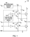
- FIG. 1 is a schematic diagram of an example of a system level circuit that includes a level shifter circuit.
- the system circuit 100 can include a top switch M T coupled to a top switch gate driver circuit 102 and a bottom switch M B coupled to a bottom switch gate driver circuit 104.
- the system circuit 100 can receive an input signal at the input IN at a first voltage domain, e.g., 0V (low) to 5V (high) and shift the signal, using the level shifter circuit 108, to a second voltage domain, e.g., 100V (low) to 105V (high), that includes the switching rail V SW and the boot-strap rail V BST .
- a first voltage domain e.g., 0V (low) to 5V (high
- a second voltage domain e.g., 100V (low) to 105V (high
- the V SW voltage level is close to ground, and a bootstrap charging circuit 106 can charge the bootstrap capacitor C BST to maintain a constant voltage across V BST and V SW .
- the signal can be transmitted by the level shifter circuit 108 and applied to the top switch gate driver circuit 102 to drive the top switch M T e.g., silicon field-effect transistor (FET).
- FET silicon field-effect transistor
- the top gate node TG goes from low-to-high to turn ON the top switch M T , and V SW rises at a high dv/dt rate.
- a gallium nitride FET which shows much lower parasitic capacitances
- an even higher dv/dt occurs at V SW , which can false trigger the level shifter and cause a wrong state at nodes OUT and TG.
- the top switch M T could be on-off-on, with many incorrect output states, which can cause further failures of the power system.
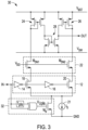
- FIG. 2 is a simplified schematic diagram of an example of a mirror-based high-voltage level shifter circuit.
- the circuit 10 can include a low-voltage metal-oxide-semiconductor (MOS) differential input section 12 that can include first and second inverter circuits 14, 16 and first and second transistors 18, 20.
- a current source 21 generating a current I S can be coupled to the first and second transistors 18, 20 and can provide a tail current.
- the circuit 10 can further include a high-voltage double-diffused MOS (DMOS) section 22 including transistors M DN1 and M DN2 , which can be coupled to the first and second transistors 18, 20, respectively.
- DMOS high-voltage double-diffused MOS
- the low voltage MOS section 12 can receive an input signal at the input IN at a first voltage domain, e.g., 0V (low) to 5V (high), and shift the signal to a second voltage domain, e.g., 100V (low) to 105V (high), that includes the switching rail V SW and the boot-strap rail V BST .
- a first voltage domain e.g., 0V (low) to 5V (high
- a second voltage domain e.g., 100V (low) to 105V (high
- the high-voltage DMOS transistors M DN1 and M DN2 can provide high-voltage isolation, while the differential input structure supports a low dv/dt immunity.
- the parasitic capacitances C PAR1 , C PAR2 can trigger high dv/dt current I DVDT at the two respective paths shown. Due to a mismatch of the parasitic capacitances and current mirrors, the high dv/dt current I DVDT can cause a false trigger of the output signal at OUT.
- the level shifter circuit 10 can consume a static current of I S .
- FIG. 3 is a simplified schematic diagram of another example of a mirror-based high-voltage level shifter circuit.
- the circuit 30 of FIG. 3 can include at least some components that are similar to those shown in FIG. 3 , which for purposes of conciseness, will not be described in detail again.
- the circuit 30 can include a pulse generator circuit 32 coupled to the differential input circuit and configured to reduce a propagation delay of the level shifter circuit.
- the pulse generator circuit can generate a pulse, e.g., 2-6ns pulse, that can dramatically increase the tail current for a high slew rate during signal transition.
- the parasitic capacitances C PAR1 , C PAR2 shown in FIG. 2
- the rail V SW can ring after pulse expires and the dv/dt immunity can remain low, similar to the circuit 10 in FIG. 2 .
- the level shifter circuit 30 can consume a static current of I S .
- FIG. 4 is a simplified schematic diagram of an example of a latch-based high-voltage level shifter circuit.
- the circuit 40 can include a differential input section 42 that can include first and second inverter circuits 44, 46 and first and second transistors M N1 , M N2 .
- the circuit 40 can further include transistors M D1 and M D2 , which can be coupled to the first and second transistors M N1 , M N2 .
- the six transistors M N3 , M N4 , and M D3 -M D6 can form a latch.
- the level shift circuit 40 of FIG. 4 can consume nearly zero static current in steady state. However, it can include six or more high-voltage DMOS transistors (M D1 - M D6 ) and can have a large footprint, especially at voltages of 100V or higher.
- M D1 - M D6 high-voltage DMOS transistors
- the parasitic capacitance C PAR1 , C PAR2 at the drains of M D1 and M D2 can trigger two respective high dv/dt currents. These dv/dt currents can reset the state of the latch, which can lead to a false-trigger of output state.
- the latch device sizes can be large to increase the strength of the latch.
- it can take a large die size and a high instant current to transmit the level-shifting signals, leading to a long propagation delay.
- CMTI common-mode transient immunity
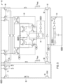
- FIG. 5 is a schematic diagram of an example of a high-voltage level shifter circuit using various techniques of this disclosure, according to the invention.
- the level shifter circuit 50 of FIG. 5 can include a differential input and isolation stage 52, e.g., high-voltage LDMOS-based, a pulse generator circuit 54 for slew rate enhancement, a dv/dt sensor and cancellation stage circuit 56, a first gain stage circuit 58, e.g., transistor-based, coupled to the dv/dt sensor and cancellation stage circuit 56, a second gain stage circuit 60, e.g., transistor-based, coupled to the first gain stage circuit 58, and an output buffer stage circuit 62.
- a differential input and isolation stage 52 e.g., high-voltage LDMOS-based
- a pulse generator circuit 54 for slew rate enhancement for slew rate enhancement
- a dv/dt sensor and cancellation stage circuit 56 e.g., a dv/dt sensor and cancellation stage circuit 56
- a first gain stage circuit 58 e.g., transistor-based, coupled to the dv/dt sensor and cancellation stage
- the first gain stage circuit 58 can include P-type (or N-type) field-effect transistors (FETs) and the second gain stage circuit 60 can include N-type (or P-type) FETs.
- FETs field-effect transistors
- the first gain stage circuit 58 can include a first common-mode gain stage and a first differential-mode gain stage, which can handle the common-mode current and differential-mode current differently.
- the second gain stage circuit 60 can include a second common-mode gain stage and second differential-mode gain stage.
- the dv/dt sensor and cancellation stage circuit 56 can be configured to reduce a common-mode current generated by a transition of the input signal from a first logic state, e.g., low, to a second logic state, e.g., high.
- the dv/dt sensor and cancellation stage circuit 56 can include a "dummy" transistor 64, e.g., LDMOS, that is the same size as the transistors 66, 68 of the differential input and isolation stage 52.
- An input signal can be received at node SIN and a corresponding level-shifted output signal can be output at node SOUT.
- a pulse e.g., a 2-ns pulse
- the pulse can generate a high tail current to transmit the differential-mode signal effectively and with a short propagation delay.
- a high dv/dt common-mode current can be generated through the drain path of the transistors 66, 68, e.g., LDMOS-based transistors, of the differential input and isolation stage 52.
- the dv/dt sensor and cancellation stage circuit 56 can include a high-voltage transistor 64, which is the same size as the transistors 66, 68 of the two main level shifting differential paths and will have a similar parasitic capacitance at its drain terminal.
- the dv/dt sensor and cancellation stage circuit 56 can sense a common-mode current generated by a transition of the input signal from a first logic state to a second logic state and generate a replica common-mode current.
- the parasitic capacitance C PAR1 , C PAR2 associated with the drain terminal of the transistor 64 will charge up via a current through node FLY_REF, which can be considered a replica common-mode current.
- the replica common-mode current through the transistor 64 can be mirrored by the current mirror formed by the transistors 72, 74.
- the transistors 72, 74 are coupled to nodes FLYP and FLYN, respectively, and those nodes receive the replica common-mode current and reduce the common-mode current to the gain stage 58.
- the current fed into nodes FLYP and FLYN by the dv/dt sensor and cancellation stage circuit 56 charges up the parasitic capacitances C PAR1 , C PAR2 associated with the drain terminals of the transistors 66, 68. Charging up the parasitic capacitances can reduce (or cancel) the common-mode current through the transistors 66, 68, which can reduce (or cancel) the common-mode current in the gain stage circuit 58.
- the dv/dt sensor and cancellation stage circuit 56 which has transistor 64 sized the same as the transistors 66, 68 of the differential input and isolation stage 52, the same amount of dv/dt current can be generated by the dv/dt sensor and cancellation stage circuit 56 and fed to the two main level shifting differential paths and reduce or cancel the dv/dt triggered common-mode current.
- a gain stage such as the first gain stage 58 (and the second gain stage 60 and more, if present) can play an important role in rejecting the common-mode signal while effectively transmitting the differential signal.
- the gain stage 58 can be coupled to the cancellation stage 56 and can be configured to receive a reduced common-mode current from the cancellation stage and a differential-mode current.
- the gain stage 58 can have a common-mode current gain of less than one.
- the differential current gain through the first gain stage 58 and the second gain stage can be at least one.
- the output stage circuit 62 can be configured to receive both the differential-mode current and the common-mode output current from the gain stage and generate a representation of the input signal shifted to the second voltage domain.
- the output stage can include a latch circuit configured to store the second logic state of the input signal to reflect the input state, e.g., after the input signal transitions from a first logic state to a second logic state.
- the first and second gains stages can include cross-coupled mirror circuits with a 1:1:1 ratio in each branch. Due to the cross-coupled structure with 1:1:1 ratio in each branch, the common-mode current gain can become one-half after the first gain stage 58 and can be further reduced to one-quarter after the second gain stage 68, as shown in FIG. 6 .
- the configuration shown in FIG. 5 is a non-limiting example configuration. In other configurations, the current gain of the first stage 58 can be greater than or less than one-half, and the current gain of the second stage 60 can be greater than or less than one-half.
- FIG. 6 is a schematic diagram of a portion of the circuit of FIG. 5 illustrating the rejection of the common-mode signal while effectively transmitting the differential signal.
- the common-mode current I CM through node FLYN (left-hand side of FIG. 6 ) is formed from the sum of the common-mode current I CM /2 through transistor 76 and the common-mode current I CM /2 through path 82 via the current mirror formed by transistor 78.
- the common-mode current I CM through node FLYP (right-hand side of FIG. 6 ) is formed from the sum of the common-mode current I CM /2 through transistor 84 and the common-mode current I CM /2 through path 86 via the current mirror formed by transistor 90.
- the cross-coupled mirror circuits with 1:1:1 ratio in the left-hand branch of the first gain stage circuit can generate a common-mode current of I CM /2 through the current mirror formed by transistors 88, 90.
- the cross-coupled structure with 1:1:1 ratio in the second gain stage circuit can further reduce the common-mode current.
- the common-mode current of I CM /2 splits between the left-hand branch and the right-hand branch of the second gain stage circuit, resulting in a common-mode current of I CM /4 through each branch.
- the common-mode current can be halved, for example, after each cross-coupled stage, from I CM to I CM /2 to I CM /4, for the non-limiting example configuration shown in FIGS. 4 and 5 .
- the common-mode current gain of the first gain stage or the second gain stage can be greater than or less than one-half.
- the differential signal is 0A through the node FLYN (left-hand side) and I DM through the node FLYP (right-hand side). Because there is no differential-mode current through the transistor 76 (left-hand side of FIG. 6 ), there is no differential-mode current flowing through the current mirror formed by transistors 88, 90 and thus no cancellation of the differential-mode current I DM via cross-coupling in the way that the common-mode current was canceled. Instead, the differential-mode current I DM through the transistor 84 can be mirrored in a 1:1:1 ratio with the current mirror formed by transistors 78, 80 and outputted to the second gain stage circuit (shown at 60 in FIG. 5 ) with a gain of one or more, for example. The second gain stage circuit can receive the differential-mode signal I DM via the current mirror formed by the transistors 92, 94 and output a differential-mode signal with a gain of at least one, for example.
- the differential gain of the circuit shown in FIGS. 4 and 5 can be one (or more) because the differential current I DM (the input signal) is fully mirrored without degrading.
- the pull-up and pull-down capability are both I DM at the last stage, which can fully transmit the input signal transitions.
- the differential-mode input current can be 2mA
- the dv/dt common-mode current under 100V/ns can be about 6mA (depending on the size of transistor and its parasitic capacitance).
- the remaining dv/dt triggered common-mode current can be about 1mA.
- the remaining common-mode current of 1mA can be further reduced to 0.25mA after two differential-mode and common-mode gain stages, as described above.
- the differential-mode current can remain unchanged at 2mA, which can help to effectively level-shift the signals and prevent false triggers.
- the common-mode current can be reduced to nearly zero in last stage (the cross-coupled stage 96 after the second gain stage), while the unity-gain differential-mode current can trigger the latch to transmit the input signal to the output.
- the input signal in the low-voltage rail can be effectively shifted to the high-voltage rails, while the high dv/dt common-mode transient is substantially rejected.
- nearly zero static current is needed in steady state to save power.
- additional gain stages can be constructed to further reduce the common-mode current gain to 1/2 N , where N is the stage number.
- additional stages can result in additional propagation delay.
- the high CMTI high-voltage level shifter circuit described above disclosure has several advantages. With the cross-coupled structure, the overall differential gain of the input signal is "1", while the common mode gain is 1/2 N , where N is the number of gain stages.
- the techniques described can help to effectively transmit a signal from a low-voltage domain to a high-voltage domain with short propagation delay and reject the high dv/dt transient of the common-mode signal.
- the high dv/dt sensor and cancellation circuit (shown at 56 in FIG. 5 ) can use a transistor identical to the input differential input transistor to detect a dv/dt transient at the switching node and feedback the transient to reject the common-mode transient current at the two main level shifting differential paths and reduce common-mode gain.
- the input low-voltage signal can be shifted to high-voltage rail, further triggering the latch circuit (shown at 62 in FIG. 5 ) to store the state. It can achieve 100V/0.1ns CMTI (or more) and can achieve nanosecond-level propagation delay, and consume zero quiescent current in steady state.
- Method examples described herein may be machine or computer-implemented at least in part. Some examples may include a computer-readable medium or machine-readable medium encoded with instructions operable to configure an electronic device to perform methods as described in the above examples.
- An implementation of such methods may include code, such as microcode, assembly language code, a higher-level language code, or the like. Such code may include computer readable instructions for performing various methods. The code may form portions of computer program products. Further, in an example, the code may be tangibly stored on one or more volatile, non-transitory, or nonvolatile tangible computer-readable media, such as during execution or at other times.
- tangible computer-readable media may include, but are not limited to, hard disks, removable magnetic disks, removable optical disks (e.g., compact discs and digital video discs), magnetic cassettes, memory cards or sticks, random access memories (RAMs), read only memories (ROMs), and the like.
Landscapes
- Engineering & Computer Science (AREA)
- Computer Hardware Design (AREA)
- Physics & Mathematics (AREA)
- Computing Systems (AREA)
- General Engineering & Computer Science (AREA)
- Mathematical Physics (AREA)
- Logic Circuits (AREA)
- Power Conversion In General (AREA)
Claims (12)
- Pegelverschiebungsschaltung (50), die konfiguriert ist, durch eine Differentialeingangsschaltung (52) ein Eingangssignal in einem ersten Spannungsbereich zu empfangen und das Eingangssignal in einen zweiten Spannungsbereich zu verschieben, wobei die Schaltung Folgendes umfasst:eine Unterdrückungsstufe (56), die mit der Differentialeingangsschaltung (52) gekoppelt ist, wobei die Unterdrückungsstufe einen ersten Transistor (64) umfasst, der mit einem ersten Stromspiegel (72, 74) gekoppelt ist, wobei die Differentialeingangsschaltung einen zweiten Transistor (66) und einen dritten Transistor (68) umfasst, wobei der erste Transistor (64), der zweite Transistor (66) und der dritte Transistor (68) an ihren Source-Anschlüssen verbunden sind und wobei der erste Stromspiegel konfiguriert ist, einen Strom an einem Drain-Anschluss des ersten Transistors (64) auf einen ersten Knoten, FLYN, der mit dem Drain-Anschluss des zweiten Transistors (66) gekoppelt ist, und einen zweiten Knoten, FLYP, der mit einem Drain-Anschluss des dritten Transistors (68) gekoppelt ist, zu spiegeln,wobei die Unterdrückungsschaltung konfiguriert ist zum:Erfassen eines ersten Gleichtaktstroms, der durch den Drain-Anschluss des zweiten Transistors (66) und den Drain-Anschluss des dritten Transistors (68) der Differentialeingangsschaltung als Antwort auf einen Übergang eines Schaltknotens von einem ersten Spannungspegel auf einen zweiten Spannungspegel erzeugt wird, wobei der Übergang des Schaltknotens durch einen Übergang des Eingangssignals von einem ersten Logikzustand in einen zweiten Logikzustand bewirkt wird;Erzeugen eines zweiten Gleichtaktstroms durch den Drain-Anschluss des ersten Transistors (64), Spiegeln des erzeugten zweiten Gleichtaktstroms unter Verwendung des ersten Stromspiegels (72, 74) auf den ersten Knoten, FLYN, und den zweiten Knoten, FLYP, und dadurch Kombinieren des zweiten Gleichtaktstroms mit dem ersten Gleichtaktstrom, um einen verringerten Gleichtaktstrom bereitzustellen; undeine Verstärkungsstufe (58), die mit der Unterdrückungsstufe (56) gekoppelt ist, wobei die Verstärkungsstufe konfiguriert ist, einen Gegentaktstrom und den verringerten Gleichtaktstrom zu empfangen, wobei die Verstärkungsstufe eine Gleichtakt-Stromverstärkung kleiner als eins aufweist und wobei die Verstärkungsstufe eine zweite Stromspiegelschaltung umfasst, die mit einer dritten Stromspiegelschaltung (84, 80, 78) kreuzgekoppelt ist, wobei ein Drain eines diodengeschalteten Transistors (76) des zweiten Stromspiegels (76, 88, 90) mit dem ersten Knoten, FLYN, gekoppelt ist und ein Drain des diodengeschalteten Transistors (84) des dritten Stromspiegels mit dem zweiten Knoten, FLYP, gekoppelt ist; undeine Ausgangsstufe (62), die konfiguriert ist, sowohl den Gegentaktstrom als auch den Gleichtakt-Ausgangsstrom von der Verstärkungsstufe (58) zu empfangen und eine Darstellung des Eingangssignals, die in den zweiten Spannungsbereich verschoben ist, zu erzeugen.
- Pegelverschiebungsschaltung (50) nach Anspruch 1, wobei die Ausgangsstufe (62) eine Signalspeicherschaltung enthält, die konfiguriert ist, den zweiten Logikzustand des Eingangssignals zu speichern.
- Pegelverschiebungsschaltung (50) nach Anspruch 1 oder 2, wobei die Verstärkungsstufe (58) eine Gegentakt-Stromverstärkung von mindestens eins aufweist.
- Pegelverschiebungsschaltung (50) nach einem der vorhergehenden Ansprüche, wobei die Verstärkungsstufe (58) eine erste Verstärkungsstufe ist, wobei die Gleichtakt-Stromverstärkung eine erste Gleichtakt-Stromverstärkung ist, wobei die Pegelverschiebungsschaltung (50) ferner Folgendes umfasst:
eine zweite Verstärkungsstufe (60), die mit einem Ausgang der ersten Verstärkungsstufe (58) gekoppelt ist, wobei die zweite Verstärkungsstufe (60) eine zweite Gleichtakt-Stromverstärkung kleiner als eins aufweist, und wahlweise wobei:(i) die erste Gleichtakt-Stromverstärkung einhalb ist und wobei die zweite Gleichtakt-Stromverstärkung einhalb ist;(ii) die erste Verstärkungsstufe (58) eine erste Gleichtakt-Verstärkungsstufe und eine erste Gegentakt-Verstärkungsstufe enthält und die zweite Verstärkungsstufe (60) eine zweite Gleichtakt-Verstärkungsstufe und eine zweite Gegentakt-Verstärkungsstufe enthält. - Pegelverschiebungsschaltung (50) nach einem der vorhergehenden Ansprüche, wobei die Verstärkungsstufe (58) eine erste Verstärkungsstufe einer Anzahl von N Verstärkungsstufen ist, wobei die einzelnen der N Verstärkungsstufen entsprechende Gleichtakt-Stromverstärkungen kleiner als eins aufweisen.
- Pegelverschiebungsschaltung (50) nach Anspruch 5, wobei die Gleichtaktverstärkung von mindestens einer der N Verstärkungsstufen 1/2N ist und wahlweise wobei die Gegentakt-Stromverstärkung mindestens eins ist.
- Pegelverschiebungsschaltung (50) nach einem der vorhergehenden Ansprüche, die ferner Folgendes umfasst:
eine Impulsgeneratorschaltung (54), die mit der Differentialeingangsschaltung (52) gekoppelt ist, um eine Ausbreitungsverzögerung der Pegelverschiebungsschaltung (50) zu verringern, wobei der Impulsgenerator konfiguriert ist, einen Impuls zu erzeugen, um einen nacheilenden Strom durch eine Stromquelle (70), die mit den Source-Anschlüssen des zweiten und des dritten Transistors der Differentialeingangsschaltung gekoppelt ist, während des Übergangs des Eingangssignals zu erhöhen. - Verfahren zum Verschieben eines Eingangssignals in einem ersten Spannungsbereich in einen zweiten Spannungsbereich, wobei das Verfahren Folgendes umfasst:Erfassen, unter Verwendung einer Unterdrückungsstufe (56), die mit einer Differentialeingangsschaltung (52) gekoppelt ist, eines ersten Gleichtaktstroms, der als Antwort auf einen Übergang eines Schaltknotens von einem ersten Spannungspegel auf einen zweiten Spannungspegel erzeugt wird, wobei der Übergang des Schaltknotens durch einen Übergang des Eingangssignals von einem ersten Logikzustand in einen zweiten Logikzustand bewirkt wird, wobei die Unterdrückungsstufe (56) einen ersten Transistor (64) umfasst, der mit einem Stromspiegel (72, 74) gekoppelt ist, die Differentialeingangsschaltung einen zweiten Transistor (66) und einen dritten Transistor (68) umfasst, wobei der erste Transistor (64), der zweite Transistor (66) und der dritte Transistor (68) an ihren Source-Anschlüssen verbunden sind und wobei der erste Stromspiegel konfiguriert ist, einen Strom an einem Drain-Anschluss des ersten Transistors (64) auf einen ersten Knoten, FLYN, der mit dem Drain-Anschluss des zweiten Transistors (66) gekoppelt ist, und auf einen zweiten Knoten, FLYP, der mit einem Drain-Anschluss des dritten Transistors (68) gekoppelt ist, zu spiegeln;Erzeugen, unter Verwendung der Unterdrückungsstufe (56), eines zweiten Gleichtaktstroms durch den Drain-Anschluss des ersten Transistors (64) und Spiegeln, unter Verwendung des Stromspiegels (72, 74), der mit dem ersten Transistor (64) gekoppelt ist, des zweiten Gleichtaktstroms auf den ersten Knoten, FLYN, und den zweiten Knoten, FLYP, dadurch Kombinieren des zweiten Gleichtaktstroms mit dem ersten Gleichtaktstrom, um einen verringerten Gleichtaktstrom bereitzustellen;Empfangen, durch eine Verstärkungsstufe (58), des verringerten Gleichtaktstroms und eines Gegentaktstroms und Erzeugen, unter Verwendung der Verstärkungsstufe (58), eines Gleichtakt-Ausgangsstroms der Verstärkungsstufe, wobei die Verstärkungsstufe (58) eine Gleichtakt-Stromverstärkung kleiner als eins aufweist und wobei die Verstärkungsstufe eine zweite Stromspiegelschaltung umfasst, die mit einer dritten Stromspiegelschaltung kreuzgekoppelt ist, wobei ein Drain eines diodengeschalteten Transistors (76) des zweiten Stromspiegels (76, 88, 90) mit dem ersten Knoten, FLYN, gekoppelt ist und ein Drain des diodengeschalteten Transistors (84) des dritten Stromspiegels mit dem zweiten Knoten, FLYP, gekoppelt ist; undEmpfangen, unter Verwendung einer Ausgangsstufe (62), des Gegentaktstroms und des Gleichtakt-Ausgangsstroms von der Verstärkungsstufe (58) und Erzeugen einer Darstellung des Eingangssignals, die in den zweiten Spannungsbereich verschoben ist.
- Verfahren nach Anspruch 8, das ferner Folgendes umfasst:
Speichern des zweiten Logikzustands des Eingangssignals. - Verfahren nach Anspruch 8 oder 9, das ferner Folgendes umfasst:
Erzeugen eines Gegentakt-Ausgangsstroms der Verstärkungsstufe, wobei die Verstärkungsstufe (58) eine Gegentakt-Stromverstärkung von mindestens eins aufweist. - Verfahren nach einem der Ansprüche 8-10, wobei die Verstärkungsstufe eine erste Verstärkungsstufe (58) ist, wobei der Gleichtakt-Ausgangsstrom der Verstärkungsstufe ein Gleichtakt-Ausgangsstrom der ersten Verstärkungsstufe ist und wobei die Gleichtakt-Stromverstärkung eine erste Gleichtakt-Stromverstärkung ist, wobei das Verfahren ferner Folgendes umfasst:
Empfangen, durch eine zweite Verstärkungsstufe (60), des Gleichtakt-Ausgangsstroms der ersten Verstärkungsstufe und Erzeugen eines Gleichtakt-Ausgangsstroms der zweiten Verstärkungsstufe, wobei die zweite Verstärkungsstufe eine zweite Gleichtakt-Stromverstärkung kleiner eins aufweist, und wahlweise wobei die erste Gleichtakt-Stromverstärkung einhalb ist und wobei die zweite Gleichtakt-Stromverstärkung einhalb ist. - Verfahren nach einem der Ansprüche 8-11, das ferner Folgendes umfasst:
Erzeugen unter Verwendung einer Impulsgeneratorschaltung (54) eines Impulses, um einen nacheilenden Strom durch eine Stromquelle (70), die mit den Source-Anschlüssen des zweiten und des dritten Transistors der Differentialeingangsschaltung (52) gekoppelt ist, während des Übergangs des Eingangssignals zu erhöhen, um eine Ausbreitungsverzögerung der Pegelverschiebungsschaltung zu verringern.
Applications Claiming Priority (1)
| Application Number | Priority Date | Filing Date | Title |
|---|---|---|---|
| US16/577,556 US10868536B1 (en) | 2019-09-20 | 2019-09-20 | High common-mode transient immunity high voltage level shifter |
Publications (2)
| Publication Number | Publication Date |
|---|---|
| EP3796557A1 EP3796557A1 (de) | 2021-03-24 |
| EP3796557B1 true EP3796557B1 (de) | 2025-04-09 |
Family
ID=72266179
Family Applications (1)
| Application Number | Title | Priority Date | Filing Date |
|---|---|---|---|
| EP20193036.9A Active EP3796557B1 (de) | 2019-09-20 | 2020-08-27 | Hochspannungspegelumsetzer mit hoher gleichtakt-transientenimmunität (cmti) |
Country Status (4)
| Country | Link |
|---|---|
| US (1) | US10868536B1 (de) |
| EP (1) | EP3796557B1 (de) |
| JP (1) | JP7242616B2 (de) |
| CN (1) | CN112543020B (de) |
Families Citing this family (8)
| Publication number | Priority date | Publication date | Assignee | Title |
|---|---|---|---|---|
| CN113472185B (zh) * | 2021-07-05 | 2022-04-22 | 电子科技大学 | 一种适用于高压GaN半桥栅驱动系统的电平移位电路 |
| US12463647B2 (en) | 2022-11-24 | 2025-11-04 | Nxp B.V. | Level shifter and multi-voltage-domain circuits |
| US12362752B2 (en) * | 2023-01-03 | 2025-07-15 | Texas Instruments Incorporated | Transient insensitive level shifter |
| US12580570B2 (en) * | 2023-11-29 | 2026-03-17 | Infineon Technologies Austria Ag | Level shifter having a cross-coupled current mirror circuit for reducing or cancelling common mode slew current |
| CN118041339B (zh) * | 2024-02-26 | 2024-08-23 | 上海帝迪集成电路设计有限公司 | 一种具有瞬态抑制功能的高压电平位移电路及其位移方法 |
| US12597928B2 (en) * | 2024-03-11 | 2026-04-07 | Infineon Technologies Austria Ag | Level shifter for power electronics circuits |
| WO2025220492A1 (ja) * | 2024-04-19 | 2025-10-23 | ローム株式会社 | 半導体装置 |
| CN121124803B (zh) * | 2025-11-14 | 2026-02-17 | 西安理工大学 | 高cmti的低延时电平移位电路 |
Family Cites Families (35)
| Publication number | Priority date | Publication date | Assignee | Title |
|---|---|---|---|---|
| US5148118A (en) | 1991-03-22 | 1992-09-15 | Linear Technology Corporation | Level shift circuit with gain enhancement |
| JP3532153B2 (ja) | 2000-12-22 | 2004-05-31 | 沖電気工業株式会社 | レベルシフタ制御回路 |
| US6611154B2 (en) * | 2001-07-02 | 2003-08-26 | International Rectifier Corporation | Circuit for improving noise immunity by DV/DT boosting |
| TWI300650B (en) * | 2003-04-24 | 2008-09-01 | Int Rectifier Corp | Fault protected self-oscillating driver |
| JP4113491B2 (ja) * | 2003-12-15 | 2008-07-09 | 三菱電機株式会社 | 半導体装置 |
| US7212033B2 (en) | 2004-03-26 | 2007-05-01 | International Rectifier Corporation | High speed transient immune differential level shifting device |
| KR101083093B1 (ko) * | 2004-09-03 | 2011-11-16 | 페어차일드코리아반도체 주식회사 | 게이트 드라이버 회로 |
| WO2009126930A2 (en) | 2008-04-11 | 2009-10-15 | Asic Advantage Inc. | Voltage level shifter |
| US7893730B2 (en) * | 2008-07-29 | 2011-02-22 | Silicon Mitus, Inc. | Level shifter and driving circuit including the same |
| US8217703B2 (en) | 2010-06-30 | 2012-07-10 | Analog Devices, Inc. | Low power fast level shifter |
| US8044699B1 (en) | 2010-07-19 | 2011-10-25 | Polar Semiconductor, Inc. | Differential high voltage level shifter |
| TWI446713B (zh) * | 2011-03-11 | 2014-07-21 | Richtek Technology Corp | 改良抗雜訊的浮接閘驅動器電路結構及其方法 |
| TWI481194B (zh) | 2012-02-10 | 2015-04-11 | Richtek Technology Corp | 浮接閘驅動器電路以及在浮接閘驅動器電路中為單端準位平移器改善抗雜訊能力的電路與方法 |
| JP5838141B2 (ja) * | 2012-02-27 | 2015-12-24 | ルネサスエレクトロニクス株式会社 | 半導体集積回路 |
| JP5825144B2 (ja) * | 2012-02-28 | 2015-12-02 | 富士電機株式会社 | 半導体装置およびハイサイド回路の駆動方法 |
| JP5900125B2 (ja) * | 2012-04-12 | 2016-04-06 | 富士電機株式会社 | 半導体基板中の寄生抵抗を利用するレベルシフト回路 |
| US8633745B1 (en) * | 2012-08-30 | 2014-01-21 | Allegro Microsystems, Llc | Circuits and related techniques for driving a high side of a half bridge circuit |
| CN105144584B (zh) * | 2013-04-18 | 2017-07-18 | 夏普株式会社 | 电平移位电路 |
| US8896377B1 (en) | 2013-05-29 | 2014-11-25 | Nxp B.V. | Apparatus for common mode suppression |
| US9960620B2 (en) | 2014-09-16 | 2018-05-01 | Navitas Semiconductor, Inc. | Bootstrap capacitor charging circuit for GaN devices |
| US9577616B2 (en) | 2015-01-19 | 2017-02-21 | Analog Devices, Inc. | Level shifter |
| US9912327B2 (en) | 2015-03-18 | 2018-03-06 | Peregrine Semiconductor Corporation | Dead time control circuit for a level shifter |
| EP3200348B1 (de) * | 2015-04-09 | 2020-10-21 | Fuji Electric Co., Ltd. | Treiberschaltung |
| JP6524829B2 (ja) * | 2015-07-13 | 2019-06-05 | 株式会社デンソー | レベルシフト回路 |
| US10819543B2 (en) | 2016-01-11 | 2020-10-27 | Texas Instruments Incorporated | Common mode transient immunity circuit for opto-isolator emulation |
| US10097183B2 (en) | 2016-03-30 | 2018-10-09 | Texas Instruments Incorporated | Level shifter and method of calibration |
| US10116301B2 (en) * | 2016-07-12 | 2018-10-30 | Infineon Technologies Americas Corp. | Cross-coupled, narrow pulse, high voltage level shifting circuit with voltage domain common mode rejection |
| CN110622418B (zh) | 2016-11-18 | 2023-06-13 | 德州仪器公司 | 具有短暂传播延迟的高压电平移位器 |
| US10523166B2 (en) * | 2017-06-07 | 2019-12-31 | Analog Devices Global | Differential amplifier with modified common mode rejection, and to a circuit with an improved common mode rejection ratio |
| US10348304B2 (en) * | 2017-09-25 | 2019-07-09 | Infineon Technologies Ag | High-voltage level-shifter circuitry |
| CN107947774B (zh) | 2017-11-17 | 2020-05-22 | 中国科学院上海微系统与信息技术研究所 | 用于IGBT栅极驱动芯片的LDMOS电平移位dv/dt噪声抑制电路 |
| US10333408B1 (en) * | 2018-04-26 | 2019-06-25 | Dialog Semiconductor (Uk) Limited | Compensation of level-shift capacitance |
| CN108288963B (zh) | 2018-04-26 | 2023-09-05 | 无锡安趋电子有限公司 | 噪声消除电路及低延时高压侧驱动电路 |
| US10483977B1 (en) * | 2018-06-08 | 2019-11-19 | Texas Instruments Incorporated | Level shifter |
| CN109905111B (zh) | 2019-03-06 | 2020-06-30 | 电子科技大学 | 适用于GaN高速栅驱动电路的电平位移电路 |
-
2019
- 2019-09-20 US US16/577,556 patent/US10868536B1/en active Active
-
2020
- 2020-08-27 EP EP20193036.9A patent/EP3796557B1/de active Active
- 2020-09-18 CN CN202010986454.6A patent/CN112543020B/zh active Active
- 2020-09-18 JP JP2020157301A patent/JP7242616B2/ja active Active
Also Published As
| Publication number | Publication date |
|---|---|
| JP2021052393A (ja) | 2021-04-01 |
| JP7242616B2 (ja) | 2023-03-20 |
| CN112543020A (zh) | 2021-03-23 |
| EP3796557A1 (de) | 2021-03-24 |
| CN112543020B (zh) | 2024-04-19 |
| US10868536B1 (en) | 2020-12-15 |
Similar Documents
| Publication | Publication Date | Title |
|---|---|---|
| EP3796557B1 (de) | Hochspannungspegelumsetzer mit hoher gleichtakt-transientenimmunität (cmti) | |
| US5969542A (en) | High speed gate oxide protected level shifter | |
| US7683668B1 (en) | Level shifter | |
| US6700429B2 (en) | Semiconductor device | |
| US9584125B2 (en) | Interface circuit | |
| US20070164789A1 (en) | High Speed Level Shift Circuit with Reduced Skew and Method for Level Shifting | |
| US11632101B1 (en) | Voltage level shifter applicable to very-low voltages | |
| US10560084B2 (en) | Level shift circuit | |
| US12388438B2 (en) | Semiconductor integrated circuit device and semiconductor system including the same | |
| US20120007660A1 (en) | Bias Current Generator | |
| US6392449B1 (en) | High-speed low-power low-offset hybrid comparator | |
| US6265896B1 (en) | Level transfer circuit for LVCMOS applications | |
| CN101401310B (zh) | 电子器件和集成电路 | |
| US10812080B2 (en) | High speed voltage level translator including an automatically bootstrapped cascode driver | |
| US7400171B1 (en) | Electronic switch having extended voltage range | |
| WO2008014383A1 (en) | Junction field effect transistor level shifting circuit | |
| US9331679B1 (en) | High-speed flying-cap level shifter | |
| EP4094357B1 (de) | Flächeneffizienter, nicht überlappender signalgenerator | |
| US10637448B1 (en) | Low-power high-speed Schmitt Trigger with high noise rejection | |
| US6329842B1 (en) | Output circuit for electronic devices | |
| US10707871B1 (en) | Capacitive level shifter | |
| US7746146B2 (en) | Junction field effect transistor input buffer level shifting circuit | |
| US6559678B1 (en) | Node predisposition circuit |
Legal Events
| Date | Code | Title | Description |
|---|---|---|---|
| PUAI | Public reference made under article 153(3) epc to a published international application that has entered the european phase |
Free format text: ORIGINAL CODE: 0009012 |
|
| STAA | Information on the status of an ep patent application or granted ep patent |
Free format text: STATUS: THE APPLICATION HAS BEEN PUBLISHED |
|
| AK | Designated contracting states |
Kind code of ref document: A1 Designated state(s): AL AT BE BG CH CY CZ DE DK EE ES FI FR GB GR HR HU IE IS IT LI LT LU LV MC MK MT NL NO PL PT RO RS SE SI SK SM TR |
|
| AX | Request for extension of the european patent |
Extension state: BA ME |
|
| STAA | Information on the status of an ep patent application or granted ep patent |
Free format text: STATUS: REQUEST FOR EXAMINATION WAS MADE |
|
| 17P | Request for examination filed |
Effective date: 20210615 |
|
| RBV | Designated contracting states (corrected) |
Designated state(s): AL AT BE BG CH CY CZ DE DK EE ES FI FR GB GR HR HU IE IS IT LI LT LU LV MC MK MT NL NO PL PT RO RS SE SI SK SM TR |
|
| STAA | Information on the status of an ep patent application or granted ep patent |
Free format text: STATUS: EXAMINATION IS IN PROGRESS |
|
| 17Q | First examination report despatched |
Effective date: 20221214 |
|
| GRAP | Despatch of communication of intention to grant a patent |
Free format text: ORIGINAL CODE: EPIDOSNIGR1 |
|
| STAA | Information on the status of an ep patent application or granted ep patent |
Free format text: STATUS: GRANT OF PATENT IS INTENDED |
|
| INTG | Intention to grant announced |
Effective date: 20241111 |
|
| GRAS | Grant fee paid |
Free format text: ORIGINAL CODE: EPIDOSNIGR3 |
|
| GRAA | (expected) grant |
Free format text: ORIGINAL CODE: 0009210 |
|
| STAA | Information on the status of an ep patent application or granted ep patent |
Free format text: STATUS: THE PATENT HAS BEEN GRANTED |
|
| AK | Designated contracting states |
Kind code of ref document: B1 Designated state(s): AL AT BE BG CH CY CZ DE DK EE ES FI FR GB GR HR HU IE IS IT LI LT LU LV MC MK MT NL NO PL PT RO RS SE SI SK SM TR |
|
| REG | Reference to a national code |
Ref country code: GB Ref legal event code: FG4D |
|
| REG | Reference to a national code |
Ref country code: CH Ref legal event code: EP |
|
| REG | Reference to a national code |
Ref country code: DE Ref legal event code: R096 Ref document number: 602020049005 Country of ref document: DE |
|
| REG | Reference to a national code |
Ref country code: IE Ref legal event code: FG4D |
|
| REG | Reference to a national code |
Ref country code: NL Ref legal event code: MP Effective date: 20250409 |
|
| PG25 | Lapsed in a contracting state [announced via postgrant information from national office to epo] |
Ref country code: NL Free format text: LAPSE BECAUSE OF FAILURE TO SUBMIT A TRANSLATION OF THE DESCRIPTION OR TO PAY THE FEE WITHIN THE PRESCRIBED TIME-LIMIT Effective date: 20250409 |
|
| REG | Reference to a national code |
Ref country code: AT Ref legal event code: MK05 Ref document number: 1784471 Country of ref document: AT Kind code of ref document: T Effective date: 20250409 |
|
| PG25 | Lapsed in a contracting state [announced via postgrant information from national office to epo] |
Ref country code: FI Free format text: LAPSE BECAUSE OF FAILURE TO SUBMIT A TRANSLATION OF THE DESCRIPTION OR TO PAY THE FEE WITHIN THE PRESCRIBED TIME-LIMIT Effective date: 20250409 Ref country code: PT Free format text: LAPSE BECAUSE OF FAILURE TO SUBMIT A TRANSLATION OF THE DESCRIPTION OR TO PAY THE FEE WITHIN THE PRESCRIBED TIME-LIMIT Effective date: 20250811 Ref country code: ES Free format text: LAPSE BECAUSE OF FAILURE TO SUBMIT A TRANSLATION OF THE DESCRIPTION OR TO PAY THE FEE WITHIN THE PRESCRIBED TIME-LIMIT Effective date: 20250409 |
|
| PGFP | Annual fee paid to national office [announced via postgrant information from national office to epo] |
Ref country code: DE Payment date: 20250724 Year of fee payment: 6 |
|
| REG | Reference to a national code |
Ref country code: LT Ref legal event code: MG9D |
|
| PG25 | Lapsed in a contracting state [announced via postgrant information from national office to epo] |
Ref country code: NO Free format text: LAPSE BECAUSE OF FAILURE TO SUBMIT A TRANSLATION OF THE DESCRIPTION OR TO PAY THE FEE WITHIN THE PRESCRIBED TIME-LIMIT Effective date: 20250709 Ref country code: GR Free format text: LAPSE BECAUSE OF FAILURE TO SUBMIT A TRANSLATION OF THE DESCRIPTION OR TO PAY THE FEE WITHIN THE PRESCRIBED TIME-LIMIT Effective date: 20250710 |
|
| PG25 | Lapsed in a contracting state [announced via postgrant information from national office to epo] |
Ref country code: PL Free format text: LAPSE BECAUSE OF FAILURE TO SUBMIT A TRANSLATION OF THE DESCRIPTION OR TO PAY THE FEE WITHIN THE PRESCRIBED TIME-LIMIT Effective date: 20250409 |
|
| PG25 | Lapsed in a contracting state [announced via postgrant information from national office to epo] |
Ref country code: BG Free format text: LAPSE BECAUSE OF FAILURE TO SUBMIT A TRANSLATION OF THE DESCRIPTION OR TO PAY THE FEE WITHIN THE PRESCRIBED TIME-LIMIT Effective date: 20250409 |
|
| PG25 | Lapsed in a contracting state [announced via postgrant information from national office to epo] |
Ref country code: HR Free format text: LAPSE BECAUSE OF FAILURE TO SUBMIT A TRANSLATION OF THE DESCRIPTION OR TO PAY THE FEE WITHIN THE PRESCRIBED TIME-LIMIT Effective date: 20250409 |
|
| PG25 | Lapsed in a contracting state [announced via postgrant information from national office to epo] |
Ref country code: AT Free format text: LAPSE BECAUSE OF FAILURE TO SUBMIT A TRANSLATION OF THE DESCRIPTION OR TO PAY THE FEE WITHIN THE PRESCRIBED TIME-LIMIT Effective date: 20250409 |
|
| PG25 | Lapsed in a contracting state [announced via postgrant information from national office to epo] |
Ref country code: RS Free format text: LAPSE BECAUSE OF FAILURE TO SUBMIT A TRANSLATION OF THE DESCRIPTION OR TO PAY THE FEE WITHIN THE PRESCRIBED TIME-LIMIT Effective date: 20250709 |
|
| PG25 | Lapsed in a contracting state [announced via postgrant information from national office to epo] |
Ref country code: IS Free format text: LAPSE BECAUSE OF FAILURE TO SUBMIT A TRANSLATION OF THE DESCRIPTION OR TO PAY THE FEE WITHIN THE PRESCRIBED TIME-LIMIT Effective date: 20250809 |
|
| PG25 | Lapsed in a contracting state [announced via postgrant information from national office to epo] |
Ref country code: LV Free format text: LAPSE BECAUSE OF FAILURE TO SUBMIT A TRANSLATION OF THE DESCRIPTION OR TO PAY THE FEE WITHIN THE PRESCRIBED TIME-LIMIT Effective date: 20250409 |
|
| REG | Reference to a national code |
Ref country code: DE Ref legal event code: R097 Ref document number: 602020049005 Country of ref document: DE |
|
| PG25 | Lapsed in a contracting state [announced via postgrant information from national office to epo] |
Ref country code: DK Free format text: LAPSE BECAUSE OF FAILURE TO SUBMIT A TRANSLATION OF THE DESCRIPTION OR TO PAY THE FEE WITHIN THE PRESCRIBED TIME-LIMIT Effective date: 20250409 Ref country code: SM Free format text: LAPSE BECAUSE OF FAILURE TO SUBMIT A TRANSLATION OF THE DESCRIPTION OR TO PAY THE FEE WITHIN THE PRESCRIBED TIME-LIMIT Effective date: 20250409 |
|
| PG25 | Lapsed in a contracting state [announced via postgrant information from national office to epo] |
Ref country code: CZ Free format text: LAPSE BECAUSE OF FAILURE TO SUBMIT A TRANSLATION OF THE DESCRIPTION OR TO PAY THE FEE WITHIN THE PRESCRIBED TIME-LIMIT Effective date: 20250409 |
|
| PG25 | Lapsed in a contracting state [announced via postgrant information from national office to epo] |
Ref country code: EE Free format text: LAPSE BECAUSE OF FAILURE TO SUBMIT A TRANSLATION OF THE DESCRIPTION OR TO PAY THE FEE WITHIN THE PRESCRIBED TIME-LIMIT Effective date: 20250409 |
|
| PG25 | Lapsed in a contracting state [announced via postgrant information from national office to epo] |
Ref country code: SK Free format text: LAPSE BECAUSE OF FAILURE TO SUBMIT A TRANSLATION OF THE DESCRIPTION OR TO PAY THE FEE WITHIN THE PRESCRIBED TIME-LIMIT Effective date: 20250409 Ref country code: RO Free format text: LAPSE BECAUSE OF FAILURE TO SUBMIT A TRANSLATION OF THE DESCRIPTION OR TO PAY THE FEE WITHIN THE PRESCRIBED TIME-LIMIT Effective date: 20250409 |
|
| PG25 | Lapsed in a contracting state [announced via postgrant information from national office to epo] |
Ref country code: IT Free format text: LAPSE BECAUSE OF FAILURE TO SUBMIT A TRANSLATION OF THE DESCRIPTION OR TO PAY THE FEE WITHIN THE PRESCRIBED TIME-LIMIT Effective date: 20250409 |
|
| PLBE | No opposition filed within time limit |
Free format text: ORIGINAL CODE: 0009261 |
|
| STAA | Information on the status of an ep patent application or granted ep patent |
Free format text: STATUS: NO OPPOSITION FILED WITHIN TIME LIMIT |
|
| REG | Reference to a national code |
Ref country code: CH Ref legal event code: L10 Free format text: ST27 STATUS EVENT CODE: U-0-0-L10-L00 (AS PROVIDED BY THE NATIONAL OFFICE) Effective date: 20260218 |
|
| 26N | No opposition filed |
Effective date: 20260112 |
|
| REG | Reference to a national code |
Ref country code: CH Ref legal event code: H13 Free format text: ST27 STATUS EVENT CODE: U-0-0-H10-H13 (AS PROVIDED BY THE NATIONAL OFFICE) Effective date: 20260324 |
|
| PG25 | Lapsed in a contracting state [announced via postgrant information from national office to epo] |
Ref country code: MC Free format text: LAPSE BECAUSE OF FAILURE TO SUBMIT A TRANSLATION OF THE DESCRIPTION OR TO PAY THE FEE WITHIN THE PRESCRIBED TIME-LIMIT Effective date: 20250409 |
|
| PG25 | Lapsed in a contracting state [announced via postgrant information from national office to epo] |
Ref country code: LU Free format text: LAPSE BECAUSE OF NON-PAYMENT OF DUE FEES Effective date: 20250827 |