EP3798809B1 - Circuit de détection de capacité, puce de détection, et dispositif électronique - Google Patents
Circuit de détection de capacité, puce de détection, et dispositif électronique Download PDFInfo
- Publication number
- EP3798809B1 EP3798809B1 EP19917529.0A EP19917529A EP3798809B1 EP 3798809 B1 EP3798809 B1 EP 3798809B1 EP 19917529 A EP19917529 A EP 19917529A EP 3798809 B1 EP3798809 B1 EP 3798809B1
- Authority
- EP
- European Patent Office
- Prior art keywords
- terminal
- capacitor
- switch unit
- module
- voltage
- Prior art date
- Legal status (The legal status is an assumption and is not a legal conclusion. Google has not performed a legal analysis and makes no representation as to the accuracy of the status listed.)
- Active
Links
Images


Classifications
-
- G—PHYSICS
- G06—COMPUTING OR CALCULATING; COUNTING
- G06F—ELECTRIC DIGITAL DATA PROCESSING
- G06F3/00—Input arrangements for transferring data to be processed into a form capable of being handled by the computer; Output arrangements for transferring data from processing unit to output unit, e.g. interface arrangements
- G06F3/01—Input arrangements or combined input and output arrangements for interaction between user and computer
- G06F3/03—Arrangements for converting the position or the displacement of a member into a coded form
- G06F3/041—Digitisers, e.g. for touch screens or touch pads, characterised by the transducing means
- G06F3/044—Digitisers, e.g. for touch screens or touch pads, characterised by the transducing means by capacitive means
-
- H—ELECTRICITY
- H03—ELECTRONIC CIRCUITRY
- H03K—PULSE TECHNIQUE
- H03K17/00—Electronic switching or gating, i.e. not by contact-making and –breaking
- H03K17/94—Electronic switching or gating, i.e. not by contact-making and –breaking characterised by the way in which the control signals are generated
- H03K17/96—Touch switches
- H03K17/962—Capacitive touch switches
-
- G—PHYSICS
- G01—MEASURING; TESTING
- G01R—MEASURING ELECTRIC VARIABLES; MEASURING MAGNETIC VARIABLES
- G01R27/00—Arrangements for measuring resistance, reactance, impedance, or electric characteristics derived therefrom
- G01R27/02—Measuring real or complex resistance, reactance, impedance, or other two-pole characteristics derived therefrom, e.g. time constant
- G01R27/26—Measuring inductance or capacitance; Measuring quality factor, e.g. by using the resonance method; Measuring loss factor; Measuring dielectric constants ; Measuring impedance or related variables
- G01R27/2605—Measuring capacitance
-
- G—PHYSICS
- G06—COMPUTING OR CALCULATING; COUNTING
- G06F—ELECTRIC DIGITAL DATA PROCESSING
- G06F3/00—Input arrangements for transferring data to be processed into a form capable of being handled by the computer; Output arrangements for transferring data from processing unit to output unit, e.g. interface arrangements
- G06F3/01—Input arrangements or combined input and output arrangements for interaction between user and computer
- G06F3/03—Arrangements for converting the position or the displacement of a member into a coded form
- G06F3/041—Digitisers, e.g. for touch screens or touch pads, characterised by the transducing means
- G06F3/0416—Control or interface arrangements specially adapted for digitisers
- G06F3/0418—Control or interface arrangements specially adapted for digitisers for error correction or compensation, e.g. based on parallax, calibration or alignment
-
- H—ELECTRICITY
- H03—ELECTRONIC CIRCUITRY
- H03K—PULSE TECHNIQUE
- H03K17/00—Electronic switching or gating, i.e. not by contact-making and –breaking
- H03K17/94—Electronic switching or gating, i.e. not by contact-making and –breaking characterised by the way in which the control signals are generated
- H03K17/945—Proximity switches
- H03K17/955—Proximity switches using a capacitive detector
-
- H—ELECTRICITY
- H03—ELECTRONIC CIRCUITRY
- H03K—PULSE TECHNIQUE
- H03K2217/00—Indexing scheme related to electronic switching or gating, i.e. not by contact-making or -breaking covered by H03K17/00
- H03K2217/94—Indexing scheme related to electronic switching or gating, i.e. not by contact-making or -breaking covered by H03K17/00 characterised by the way in which the control signal is generated
- H03K2217/96—Touch switches
- H03K2217/9607—Capacitive touch switches
- H03K2217/960705—Safety of capacitive touch and proximity switches, e.g. increasing reliability, fail-safe
-
- H—ELECTRICITY
- H03—ELECTRONIC CIRCUITRY
- H03K—PULSE TECHNIQUE
- H03K2217/00—Indexing scheme related to electronic switching or gating, i.e. not by contact-making or -breaking covered by H03K17/00
- H03K2217/94—Indexing scheme related to electronic switching or gating, i.e. not by contact-making or -breaking covered by H03K17/00 characterised by the way in which the control signal is generated
- H03K2217/96—Touch switches
- H03K2217/9607—Capacitive touch switches
- H03K2217/96071—Capacitive touch switches characterised by the detection principle
- H03K2217/960725—Charge-transfer
Definitions
- Embodiments of the present disclosure relate to the technical field of capacitance detection, and specifically to a capacitance detection circuit, a detection chip, and an electronic device.
- Capacitance detection technology is widely used in electronic devices and can realize human-computer interaction.
- a capacitive touch screen on an electronic device can realize a touch control function through capacitance detection; as another example, a capacitance detection module on a headset can automatically detect whether a user is wearing the headset.
- a capacitance detection module on a headset can automatically detect whether a user is wearing the headset.
- self-capacitance during capacitance detection, when no human body approaching or touching, there is self-capacitance between a detection electrode and the circuit ground. When a human body approaches or touches the detection electrode, the capacitance between the detection electrode and the circuit ground may increase, a relevant operation of the user may be determined by detecting a change in the capacitance.
- US2018209858A1 is directed to an apparatus for detecting capacitance comprises a signal driving circuit, a conversion circuit and a cancellation circuit.
- the signal driving circuit is configured to periodically charge and discharge at least one capacitor to be detected.
- the conversion circuit is configured to convert a capacitance signal of the at least one capacitor to be detected into voltage signal.
- the cancellation circuit is configured to cancel initial capacitance of the at least one capacitor to be detected.
- the cancellation circuit is configured to cancel initial capacitance of the at least one capacitor to be detected.
- the cancellation circuit includes a first adjustable capacitor, a sixth switch, a seventh switch, and an eighth switch, a ninth switch and a second direct current voltage source.
- One end of the first adjustable capacitor is connected to the second current voltage capacitor via the sixth switch, and is grounded via the seventh switch, the other end of the first adjustable capacitor is connected to the inverting input of the first operational amplifier.
- the eight switch and the ninth switch are controlled by the first switch control signal and the inverted signal thereof and are configured to change a third switch control signal controlling the sixth switch and the seventh switch.
- the frequencies of the second and third switch control signals are twice the frequency of the first switch control signal.
- the initial capacitance (including parasitic capacitance) of a capacitor to be detected is canceled via the adjustable capacitor of the cancellation circuit, so that an output is zero when capacitance of the capacitor to be detected is not changed.
- the CN108475155A is directed to a capacitance detection circuit.
- the capacitance detection circuit includes a first driving circuit, a first cancel circuit and a programmable gain amplification PGA circuit.
- the first driving circuit, the first cancel circuit and the PGA circuit are connected to a first end of the detection capacitor, a second end of the detection capacitor is grounded, the first driving circuit is configured to perform charging and discharging on the detection capacitor, the first cancel circuit is configured to cancel a base capacitance of the detection capacitor, and the PGA circuit is configured to convert a capacitance signal of the detection capacitor after the base capacitance is cancelled into a voltage signal, the first cancel circuit includes a first cancel capacitor.
- CN107466368A is directed to a capacitance detection circuit, comprising an amplifier, a dominant pole of the amplifier being controllable, and an inverting input end of the amplifier being configured to connect to capacitor to be detected; a feedback capacitor module connected between the inverting input end of the amplifier and an output end of the amplifier, the capacitance value of the feedback capacitor module being adjustable; a feedback resistor module connected between the inverting input end of the amplifier and the output end of the amplifier, the resistance value of the feedback resistor module being adjustable; and a capacitance calculation module connected to the output end of the amplifier and configured to detect a change in value of the capacitor to be detected according to an output signal of the amplifier.
- the capacitance detection circuit has a strong anti-interference capability, and can well achieve resistance to low-frequency interference and high
- embodiments of the present disclosure provide a capacitance detection circuit, a detection chip, and an electronic device to overcome or alleviate the technical defect in the existing technology.
- the objective is solved by the capacitance detection circuit as set out in claim 1.
- Preferred embodiments and advancements are set out in the dependent claims.
- the embodiments of the present disclosure provide a capacitance detection circuit, including: a first drive module, a conversion module, a processing module, and a control module; the first drive module is configured to charge a first capacitor to be detected; the conversion module is configured to perform charge conversion processing on the first capacitor to be detected to generate an output voltage, the conversion module including a first suppression module, the control module is configured to control the first suppression module to suppress an interference signal with a frequency that is less than a first frequency or greater than a second frequency when the conversion module generates the output voltage, and the second frequency is greater than the first frequency; and the processing module is configured to determine a capacitance change before and after the first capacitor to be detected is affected by an applied electric field based on the output voltage.
- an embodiment of the present disclosure provides a detection chip, including: the capacitance detection circuit according to any one of the embodiments in the first aspect.
- an embodiment of the present disclosure provides an electronic device, including: the detection chip according to the second aspect.
- the capacitance detection circuit, the detection chip, and the electronic device of the embodiments of the present disclosure suppress the interference signal with the frequency that is less than the first frequency or greater than the second frequency using the first suppression module, when the output voltage is generated by the conversion module, thereby reducing the influence of the interference signal, and improving the sensitivity and accuracy of capacitance detection.
- the capacitance detection circuit provided in the embodiments of the present disclosure may be applied to self-capacitance detection and mutual capacitance detection. To this end, in the following embodiments, the capacitance detection circuit applied to self-capacitance detection is first described, and then, the connection of the capacitance detection circuit in mutual capacitance detection will be described.
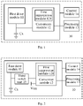
- Fig. 1 is a structural diagram of a capacitance detection circuit provided by an illustrative example of the present disclosure.
- the capacitance detection circuit 10 includes: a first drive module 11, a conversion module 12, a processing module 13, and a control module 14; the first drive module 11 is configured to charge a first capacitor to be detected Cx; the conversion module 12 is configured to perform charge conversion processing on the first capacitor to be detected to generate an output voltage, the conversion module 12 including a first suppression module 121, the control module 14 is configured to control the first suppression module 121 to suppress an interference signal with a frequency that is less than a first frequency or greater than a second frequency when the conversion module 12 generates the output voltage, and the second frequency is greater than the first frequency; and the processing module 13 is configured to determine a capacitance change before and after the first capacitor to be detected is affected by an applied electric field based on the output voltage.
- the first drive module 11 charges the first capacitor to be detected
- the conversion module 12 performs charge conversion processing on the first capacitor to be detected to generate the output voltage
- the conversion module 12 performs conversion processing on charge transferred by the first capacitor to be detected to generate the output voltage.
- the first suppression module 121 suppresses a signal with a frequency that is less than the first frequency or greater than the second frequency.
- Fig. 2 is a structural diagram of a capacitance detection circuit provided by an illustrative example of the present disclosure.
- the capacitance detection circuit 10 further includes a third switch unit 15, and the third switch unit 15 is connected between the first drive module 11 and a first input terminal of the conversion module 12.
- the third switch unit 15 When the third switch unit 15 is turned off, the first drive module 11 charges the first capacitor to be detected, and when the third switch unit 15 is turned on, the conversion module 12 performs charge conversion processing on the first capacitor to be detected to generate the output voltage.
- the third switch unit 15 when the third switch unit 15 is turned on, it is a charge transfer phase.
- the third switch unit 15 may be a single-pole single-throw switch, and when the third switch unit 15 is connected to the first capacitor to be detected and the conversion module 12, it is the charge transfer phase.
- the first drive module 11 is also equipped with a switch, and in a charging phase, the first drive module 11 and the first capacitor to be detected are connected, in this regard, the third switch unit 15 is turned off; in the charge transfer phase, the switch of the first drive module 11 is turned off, so that the first drive module 11 and the first capacitor to be detected are disconnected, and in this regard, the third switch unit 15 is turned on.
- the present disclosure is limited herein.
- the conversion module 12 has a first input terminal and a second input terminal, the first input terminal of the conversion module 12 is electrically connected to the first drive module 11, and the second input terminal of the conversion module 12 is connected to a common mode voltage and/or is connected to other circuits that capable to equivalently generate the common mode voltage.
- the conversion module 12 2. includes a differential amplifier.
- the differential amplifier may be a single-ended differential amplifier 122 or a double-ended differential amplifier 123.
- two specific application scenarios are listed to illustrate the situations where the conversion module 12 respectively includes the single-ended differential amplifier 122 and the double-ended differential amplifier 123.
- Fig. 3 is a structural diagram of a capacitance detection circuit provided by an embodiment of the present disclosure.
- the first input terminal of the conversion module 12 is an inverting input terminal of the single-ended differential amplifier 122
- the second input terminal of the conversion module 12 is a non-inverting input terminal of the single-ended differential amplifier 122
- the first drive module 11 is electrically connected to the inverting input terminal of the single-ended differential amplifier 122
- the non-inverting input terminal of the single-ended differential amplifier 122 is connected to the common mode voltage
- an output terminal of the single-ended differential amplifier 122 is electrically connected to the processing module 13
- two terminals of the first suppression module 121 are respectively connected to the inverting input terminal and the output terminal of the single-ended differential amplifier 122.
- the conversion module 12 includes the single-ended differential amplifier 122 is used as an example for description.
- the first suppression module 121 includes a first switch unit 1211, a first capacitor 1212, and a second capacitor 1213; a first terminal and a second terminal of the first switch unit 1211 are respectively connected to the inverting input terminal and the output terminal of the single-ended differential amplifier 122, the first capacitor 1212 is respectively connected to the first terminal of the first switch unit 1211 and the second terminal of the first switch unit 1211 through a third terminal of the first switch unit 1211, a second terminal of the first capacitor 1212 is grounded, and two terminals of the second capacitor 1213 are respectively connected to the inverting input terminal and the output terminal of the single-ended differential amplifier 122.
- the control module 14 is configured to control the first switch unit 1211 to switch back and forth between the first terminal and the second terminal, so that the third terminal of the first switch unit 1211 is connected to the first terminal or the third terminal is connected to the second terminal, a switching frequency of the first switch unit 1211 is greater than twice a driving frequency (i.e., the driving frequency of the first drive module 11), to suppress an electrical signal with a frequency less than the first frequency.
- the control module 14 controls the first switch unit 1211 to switch back and forth between the first terminal and the second terminal, so that the third terminal of the first switch unit 1211 is connected to the first terminal or the third terminal is connected to the second terminal, to perform reset processing on the second capacitor 1213.
- the driving frequency i.e., the driving frequency of the first drive module 11
- the driving frequency refers to the switching frequency at which the third switch unit 15 is turned on and turned off.
- the first suppression module 121 suppresses the electrical signal with the frequency less than the first frequency mainly for the interference signal generated by the power supply.
- the interference signal generated by the power supply is within 50Hz. Therefore, the first frequency may be 50Hz.
- here is only an exemplary description.
- the first switch unit 1211 may include a single-pole double-throw switch, to switch back and forth between the first terminal and the second terminal, so that the third terminal of the first switch unit 1211 is connected to the first terminal or the third terminal is connected to the second terminal.
- the first switch unit 1211 includes two single-pole single-throw switches, one single-pole single-throw switch is turned on, and the other single-pole single-throw switch is turned off, that is, the two single-pole single-throw switches are alternately turned on and turned off to function as one single-pole double-throw switch.
- the combination of the second capacitor 1213, the first switch unit 1211 and the first capacitor 1212 adds a zero point F 0 to the capacitance detection circuit 10, and this zero point may be directly used as the first frequency.
- Fig. 4 is a schematic diagram of an amplitude-frequency characteristic provided by an embodiment of the present disclosure. The gain of a signal before the zero point decreases as the frequency decreases, and the amplitude-frequency response after the zero point is flat.
- the gain of the capacitance detection circuit 10 may be increased, for example, the capacitance value C f of the second capacitor 1213 may be reduced.
- Fig. 5 is a structural diagram of a capacitance detection circuit provided by an embodiment of the present disclosure.
- the first drive module 11 includes a fourth switch unit 112, and the control module 14 is further configured to control the fourth switch unit 112 to be in a first closed state so that the first drive module 11 charges the first capacitor to be detected; specifically, since when the fourth switch unit 112 is in the first closed state, a first terminal of the first capacitor to be detected is connected to a first voltage (Vcc) through the fourth switch unit 112, a second terminal of the first capacitor to be detected is connected to a second voltage (such as gnd), and the first voltage is greater than the second voltage, thereby realizing charging the first capacitor to be detected.
- Vcc first voltage
- gnd second voltage
- Fig. 5a is a structural diagram of a capacitance detection circuit provided by an embodiment of the present disclosure.
- the fourth switch unit 112 includes a fourth switch K 4 , the fourth switch K 4 is a single-pole single-throw switch, one terminal of the fourth switch K 4 is connected to the first voltage (Vcc), and the other terminal of the fourth switch K 4 is connected to the first capacitor to be detected.
- the fourth switch K 4 is turned on, the fourth switch unit 112 is in the first closed state.
- the two terminals of the first capacitor to be detected are connected to the first voltage (Vcc) and the second voltage (such as gnd) respectively, realizing charging the first capacitor to be detected.
- control module 14 is further configured to control the fourth switch unit 112 to be in a second closed state to discharge the first capacitor to be detected; specifically, since when the fourth switch unit 112 is in the second closed state, the first terminal of the first capacitor to be detected is connected to a third voltage (Vss) through the fourth switch unit 112, the second terminal of the first capacitor to be detected is connected to the second voltage, and the second voltage is higher than the third voltage, thereby discharging the first capacitor to be detected.
- Vss third voltage
- the fourth switch unit 112 has two closed states, it can offset high-correlation noise, mainly low-frequency noise in the circuit, thereby significantly improving the signal-to-noise ratio.
- the fourth switch unit 112 may include a single-pole double-throw switch, realizing two closed states by connecting two connecting terminals, or the fourth switch unit 112 may include two single-pole single-throw switches, the first single-pole single-throw switch is turned on, and the second single-pole single-throw switch is turned off to be the first closed state, the first single-pole single-throw switch is turned off, and the second single-pole single throw switch is turned on to be the second closed state.
- the present disclosure is limited herein.
- Fig. 5b is a structural diagram of a capacitance detection circuit provided by an embodiment of the present disclosure.
- the fourth switch unit 112 includes a fifth switch K 51 , the fifth switch K 51 is a single-pole double-throw switch, a first terminal of the fifth switch K 51 is connected to the first voltage, a second terminal of the fifth switch K 51 is connected to the third voltage, and a third terminal of the fifth switch K 51 is connected to the first capacitor to be detected.
- the fourth switch unit 112 When the first terminal and the third terminal of the fifth switch K 51 are connected, the fourth switch unit 112 is in the first closed state, and the two terminals of the first capacitor to be detected are respectively connected to the first voltage (Vcc) and the second voltage (such as gnd), realizing charging of the first capacitor to be detected; and when the second terminal and the third terminal of the fifth switch K 51 are connected, the fourth switch unit 112 is in the second closed state, and the two terminals of the first capacitor to be detected are respectively connected to the second voltage (such as gnd) and the third voltage (Vss), realizing discharging the first capacitor to be detected.
- Fig. 6 is a structural diagram of a capacitance detection circuit provided by an embodiment of the present disclosure.
- the first switch unit 1211 may include a first switch K 1 ;
- the third switch unit 15 is K 3 ;
- the fourth switch unit 112 may include a fourth switch K 4 , and may also include a fifth switch K 51 .
- the capacitance detection circuit 10 is a self-capacitance detection circuit
- the differential amplifier included in the conversion module 12 is the single-ended differential amplifier 122.
- the first drive module 11 includes the fourth switch K 4 and the fifth switch K 51 , a first terminal of the fourth switch K 4 is electrically connected to the first terminal of the first capacitor to be detected Cx, the second terminal of the first capacitor to be detected Cx is grounded (the ground voltage is the second voltage), a second terminal of the fourth switch K 4 is electrically connected to the third terminal of the fifth switch, the first terminal of the fifth switch K 51 is connected to the first voltage Vcc, and the second terminal of the fifth switch K 51 is connected to the third voltage Vss; where the fourth switch K 4 is turned on and the first terminal and the third terminal of the fifth switch K 51 are connected, and the first capacitor to be detected is connected to the first voltage Vcc, in this regard, the fourth switch unit 112 is in the first closed state; the fourth switch K 4 is turned on and the second terminal and the third
- Two terminals of the third switch unit 15K 3 are electrically connected to the first terminal of the first capacitor to be detected and the inverting input terminal of the single-ended differential amplifier 122, respectively.
- the non-inverting input terminal of the single-ended differential amplifier 122 is connected to the common mode voltage Vcm, and the output terminal of the single-ended differential amplifier 122 (that is, the first output terminal of the single-ended differential amplifier 122) is connected to the processing module 13.
- the first capacitor 1212 may be respectively connected to the first terminal of the first switch K 1 and the second terminal of the first switch K 1 through a third terminal of the first switch K 1 , the second terminal of the first capacitor 1212C r is grounded, and the two terminals of the second capacitor 1213C f are respectively connected to the inverting input terminal and the output terminal of the single-ended differential amplifier 122.
- the double-ended differential amplifier 123 has a non-inverting input terminal, an inverting input terminal, a first output terminal, and a second output terminal
- the first input terminal of the conversion module 12 is the inverting input terminal of the double-ended differential amplifier 123
- the second input terminal of the conversion module 12 is the non-inverting input terminal of the double-ended differential amplifier 123
- the first drive module 11 is electrically connected to the inverting input terminal of the double-ended differential amplifier 123
- the non-inverting input terminal of the double-ended differential amplifier 123 is connected to the common mode voltage
- the first output terminal and the second output terminal of the double-ended differential amplifier 123 are both electrically connected to the processing module 13
- two terminals of the first suppression module 121 are respectively connected to the inverting input terminal and the first output terminal of the double-ended differential amplifier 123.
- the input terminal and the output terminal of the double-ended differential amplifier 123 may be connected to only one first suppression module 121.
- the double-ended differential amplifier 123 is equivalent to the single-ended differential amplifier 122, and the input terminal and the output terminal of the double-ended differential amplifier 123 are equipped with the first suppression module 122 and a second suppression module 124 at the same time.
- the dynamic range of the detection circuit is relatively large, and a relatively large gain may be achieved, thereby improving the sensitivity of detection.
- Fig. 7 is a structural diagram of a capacitance detection circuit provided by an embodiment of the present disclosure.
- the conversion module 12 respectively including the double-ended differential amplifier 123 is used as an example for description.
- the conversion module 12 further includes a second suppression module 124, two terminals of the second suppression module 124 are respectively connected to the non-inverting input terminal and the second output terminal of the double-ended differential amplifier 123, the control module 14 is configured to control the second suppression module 124 to suppress the interference signal with the frequency that is less than the first frequency or greater than the second frequency when the conversion module 12 generates the output voltage, and the second frequency is greater than the first frequency.
- the second suppression module 124 includes a second switch unit 1241, a third capacitor 1242, and a fourth capacitor 1243; a first terminal and a second terminal of the second switch unit 1241 are respectively connected to the non-inverting input terminal and the second output terminal of the double-ended differential amplifier 123, two terminals of the fourth capacitor 1243 are respectively connected to the first terminal of the second switch unit 1241 and the second terminal of the second switch unit 1241, a first terminal of the third capacitor 1242 is electrically connected to a third terminal of the second switch unit 1241, and a second terminal of the third capacitor 1242 is grounded; and the control module 14 is configured to control the second switch unit 1241 to switch back and forth between the first terminal and the second terminal, so that the third terminal of the second switch is connected to the first terminal or the third terminal is connected to the second terminal, a switching frequency of the second switch unit 1241 is greater than twice a driving frequency, to suppress an electrical signal with a frequency less than
- the driving frequency is a switching frequency at which a switch in the second drive module is turned on or turned off, or, in a mutual capacitance detection circuit, the driving frequency is a power supply frequency of the second drive module.
- the second switch unit 1241 may include a single-pole double-throw switch, to switch back and forth between the first terminal and the second terminal, so that the third terminal of the second switch unit 1241 is connected to the first terminal or the third terminal is connected to the second terminal.
- the second switch unit 1241 may include two single-pole single-throw switches, one single-pole single-throw switch is turned on, the other single-pole single-throw switch is turned off, and two single-pole single-throw switches are alternately turned on and turned off to function as one single-pole double-throw switch.
- a single-pole double-throw switch to switch back and forth between the first terminal and the second terminal, so that the third terminal of the second switch unit 1241 is connected to the first terminal or the third terminal is connected to the second terminal.
- the second switch unit 1241 may include two single-pole single-throw switches, one single-pole single-throw switch is turned on, the other single-pole single-throw switch is turned off, and two single-pole single-throw switches are alternate
- Fig. 8 is a structural diagram of a capacitance detection circuit provided by an embodiment of the present disclosure.
- the first switch unit 1211 may include the first switch K 1 ;
- the second switch unit 1241 may include a second switch K 2 ;
- the third switch unit 15 is K 3 ;
- the fourth switch unit 112 may include a fourth switch K 4 , and may also include a fifth switch K 51 .
- the capacitance detection circuit 10 is a self-capacitance detection circuit, and the differential amplifier included in the conversion module 12 is the double-ended differential amplifier 123.
- the capacitance detection circuit 10, the first drive module 11, and the first suppression module 121 provided in the present embodiment are the same as those in Embodiment 4, and detailed description thereof will be omitted.
- the conversion module 12 in the present embodiment further includes the second suppression module 124.
- a first terminal and a second terminal of the second switch K 2 are respectively connected to the non-inverting input terminal and the second output terminal of the double-ended differential amplifier 123
- the two terminals of the fourth capacitor 1243C f are respectively connected to the first terminal of the second switch K 2 and the second terminal of the second switch K 2
- the first terminal of the third capacitor 1242C r is electrically connected to the third terminal of the second switch unit 1241
- the second terminal of the third capacitor 1242C r is grounded.
- the capacitance values of the first capacitor 1212 and the third capacitor 1242 are the same as C r
- the capacitance values of the second capacitor 1213 and the fourth capacitor 1243 are the same as C f .
- the capacitance detection circuit 10 shown in Fig. 6 and Fig. 8 is suitable for the case where the self-capacitance of the first capacitor to be detected Cx is small, because the self-capacitance is small and the influence on detection is small.
- Fig. 9 is a structural diagram of a capacitance detection circuit provided by an embodiment of the present disclosure, alternatively, in an embodiment of the present disclosure, as shown in Fig. 9 , the capacitance detection circuit 10 further includes a first offset module 16; and the control module 14 is further configured to control the first offset module 16 to charge a first offset capacitor, and to control the first offset capacitor to charge or discharge the first capacitor to be detected to perform charge offset.
- the first offset module 16 includes a fifth switch unit 161, and the control module 14 is further configured to control the fifth switch unit 161 to be in a first closed state to form a charging branch so that the offset module charges the first offset capacitor; and the control module 14 is further configured to control the fifth switch unit 161 to be in a second closed state to form an offset branch so that the first offset capacitor Cc charges or discharges the first capacitor to be detected to perform charge offset.
- the fifth switch unit 161 may include two single-pole double-throw switches, and three closed states are realized by the switching of the two single-pole double-throw switches.
- the fifth switch unit 161 may include two single-pole double-throw switches, and three closed states are realized by the switching of the two single-pole double-throw switches.
- the fifth switch unit 161 when the fifth switch unit 161 is in the first closed state, two terminals of the first offset capacitor are respectively connected to a fourth voltage and a fifth voltage, and the fifth voltage is greater than the fourth voltage. In this regard, the first offset capacitor is charged.
- a first terminal of the first offset capacitor is electrically connected to the first terminal of the first capacitor to be detected through the fifth switch unit 161
- a second terminal of the first offset capacitor is connected to a sixth voltage or a seventh voltage through the fifth switch unit 161
- the sixth voltage is less than the second voltage connected to a second terminal of the capacitor to be detected, in this regard, the first capacitor to be detected is discharged to perform charge offset
- the seventh voltage is greater than the second voltage connected to the second terminal of the capacitor to be detected, in this regard, the first capacitor to be detected is charged to perform charge offset.
- the charge on the first capacitor to be detected is transferred to the first offset capacitor, and when the first offset capacitor charges the capacitor to be detected to perform charge offset, the charge on the first offset capacitor is transferred to the first capacitor to be detected.
- the charge transfer in the offset process is to eliminate the influence caused by the existence of a basic capacitance of the first capacitor to be detected, which is different from the charge transfer in the charge transfer phase.
- the capacitance detection circuit 10 based on the self-capacitance detection shown in Fig. 3 , combined with the structure of the first drive module 11 shown in the capacitance detection circuit 10 shown in Fig. 5 , and the structure of the first offset module 16 shown in the capacitance detection circuit 10 shown in Fig. 9 , the operation sequence of the capacitance detection circuit 10 will be described.
- the capacitance detection circuit 10 is divided into a positive process and a negative process:
- the third switch unit 15 is turned off, the fourth switch unit 112 is in the first closed state, the first capacitor to be detected is connected to the first voltage, the first drive module 11 charges the first capacitor to be detected to the first voltage, the fifth switch unit 161 is in the first closed state, the two terminals of the first offset capacitor are respectively connected to the fourth voltage and the fifth voltage to form a charging branch, and the first offset capacitor is charged to the fifth voltage;
- the third switch unit 15 is still turned off, the fourth switch unit 112 is turned off, the fifth switch unit 161 is in the second closed state, in this regard, the first offset capacitor discharges the first capacitor to be detected to perform charge offset, and part of the charge of the first capacitor to be detected transfers to the first offset capacitor; and in the third phase, the third switch unit 15 is turned on, the first capacitor to be detected is connected to the
- the third switch unit 15 is turned off, the fourth switch unit 112 is in the second closed state, the first capacitor to be detected is discharged to the third voltage, the fifth switch unit 161 is in the first closed state, the two terminals of the first offset capacitor are respectively connected to the fourth voltage and the fifth voltage to form a charging branch, and the first offset capacitor is charged to the fifth voltage;
- the third switch unit 15 is still turned off, the fourth switch unit 112 is turned off, the fifth switch unit 161 is in the second closed state, in this regard, the first offset capacitor charges the first capacitor to be detected to perform charge offset, part of the charge of the first offset capacitor transfers to the first capacitor to be detected, and the first capacitor to be detected is charged to the seventh voltage; and in the third phase, the third switch unit 15 is turned on, the first capacitor to be detected is connected to the conversion module 12, the fourth switch unit 112 is turned off, the fifth switch unit 161 is in the second closed state, the conversion module 12 performs charge conversion processing on the first capacitor to be detected
- the first offset capacitor may discharge or charge the first capacitor to be detected to the common mode voltage Vcm; if there is no finger approaching, the capacitance value Cx of the first capacitor to be detected may not change.
- the output of the conversion module 12 may not change (zero); if an object approaches the first capacitor to be detected, Cx may change, which is recorded as Cx+ ⁇ C, where ⁇ C is the capacitance change caused by the object approaching the first capacitor to be detected. As the first capacitor to be detected becomes larger, the output of the conversion module 12 may change (not zero) during the third phase of detection.
- Fig. 10 is a structural diagram of a capacitance detection circuit provided by an embodiment of the present disclosure, in the present embodiment, the capacitance detection circuit 10 is a self-capacitance detection circuit, and the differential amplifier included in the conversion module 12 is the single-ended differential amplifier 122.
- the capacitance detection circuit 10 is a self-capacitance detection circuit
- the differential amplifier included in the conversion module 12 is the single-ended differential amplifier 122.
- the first switch unit 1211 may include the first switch K 1 ; the second switch unit 1241 may include the second switch K 2 ; the third switch unit 15 is K 3 ; the fourth switch unit 112 may include a fourth switch K4, and may also include a fifth switch K 51 ; the fifth switch unit 161 may include three fifth switches K 52 , K 53 , and K 54 , and may also include two sixth switches K 61 and K 62 ; and a seventh switch unit 171 may include a seventh switch K 7 , and may also include an eighth switch K 51 .
- the capacitance detection circuit in Fig. 10 includes the first drive module 11, the conversion module 12, the first suppression module 121 and the first offset module 16.
- the first drive module 11, the conversion module 12, and the first suppression module 121 are the same as those in Embodiment 4.
- the fifth switch unit 161 includes three fifth switches K 52 , K 53 , and K 54 , and two sixth switches K 61 and K 62 .
- the fourth voltage and the sixth voltage are both Vss
- the fifth voltage and the seventh voltage are both Vcc.
- the fifth switch K 52 may connect the first terminal and the third terminal or connect the second terminal and the third terminal by switching between the first terminal and the second terminal.
- the first terminal of the fifth switch K 52 is connected to Vss
- a second terminal of the fifth switch K 52 is connected to Vcc
- the third terminal of the fifth switch K 52 is connected to a first terminal of the sixth switch K 61
- a second terminal of the sixth switch K 61 is connected to the first terminal of the first capacitor to be detected Cx
- a third terminal of the sixth switch K 61 is electrically connected to the first terminal of the first offset capacitor Cc
- the sixth switch K 61 may connect the first terminal and the third terminal or connect the second terminal and the third terminal by switching between the first terminal and the second terminal.
- the second terminal of the first offset capacitor Cc is electrically connected to a third terminal of the sixth switch K 62 , and the sixth switch K 62 may connect the first terminal and the third terminal or connect the second terminal and the third terminal by switching between the first terminal and the second terminal.
- a first terminal of the sixth switch K 62 and a third terminal of the fifth switch K 53 are electrically connected, and the first terminal of the sixth switch K 62 and a third terminal of the fifth switch K 54 are electrically connected.
- the fifth switch K 53 may connect the first terminal and the third terminal or connect the second terminal and the third terminal by switching between the first terminal and the second terminal
- the fifth switch K 54 may connect the first terminal and the third terminal or connect the second terminal and the third terminal by switching between the first terminal and the second terminal
- the first terminal of the fifth switch K 53 is connected to Vcc
- a second terminal of the fifth switch K 53 is connected to Vss
- the first terminal of the fifth switch K 54 is connected to Vss
- a second terminal of the fifth switch K 54 is connected to Vss.
- the fifth switches (K 52 , K 53 , and K 54 ) are all switched to the first terminal, connecting their respective first and third terminals, and the sixth switches (K 61 and K 62 ) are all switched to the first terminal, connecting their respective first and third terminals, in this regard, the fifth switch unit 161 is in the first closed state; the fifth switches (K 52 , K 53 , and K 54 ) are all switched to the first terminal, connecting their respective first and third terminals, and the sixth switches (K 61 and K 62 ) are all switched to the second terminal, connecting their respective second and third terminals, in this regard, the fifth switch unit 161 is in the second closed state; the fifth switches (K 52 , K 53 , and K 54 ) are all switched to the second terminal, connecting their respective first and third terminals, and the sixth switches (K 61 and K 62 ) are all switched to the first terminal, connecting their respective first and third terminals, in this regard, the fifth switch unit 161 is in the first closed state; and the fifth switches
- Fig. 11 is a control sequence diagram provided by an embodiment of the present disclosure. Based on Vcc or Vss connected to the first capacitor to be detected, the capacitance detection circuit 10 is divided into a positive process and a negative process: For the positive process, corresponding to T 1 period in Fig. 11 , all the fifth switches (K 51 , K 52 , K 53 and K 54 ) in the positive process are switched to the first terminal, connecting their respective first and third terminals, the first switch K 1 and the second switch K 2 are periodically turned on and turned off, for the first phase (t 1 period in Fig.
- the switching frequency of the first switch unit 1211 is greater than twice the power supply frequency, to suppress the signal with the frequency that is less than the first frequency or greater than the second frequency.
- the capacitance detection circuit is a self-capacitance circuit, and the power supply frequency refers to the switching frequency at which the third switch unit 15 is turned on and turned off.
- the turn-on or turn-off of the third switch unit 16 is controlled by the fourth switch K 4 .
- the first switch unit 1211 is the first switch K 1 .
- the switching frequency of the first switch unit 1211 being greater than twice the power supply frequency means that the switching frequency of the first switch K 1 between the first terminal and the second terminal is greater than twice the switching frequency at which the fourth switch K 4 is turned on and turned off.
- Fig. 12 is a structural diagram of a capacitance detection circuit provided by an embodiment of the present disclosure.
- the capacitance detection circuit 10 is a self-capacitance detection circuit, and the differential amplifier included in the conversion module 12 is the double-ended differential amplifier 123.
- the capacitance detection circuit 10 in the present embodiment includes the first drive module 11, the conversion module 12, the first suppression module 121, the first offset module 16 and the second suppression module 124.
- the first drive module 11, the conversion module 12, the first suppression module 121, and the first offset module 16 are the same as those in Embodiment 6, and detailed description thereof will be omitted.
- the first terminal and the second terminal of the second switch K 2 are respectively connected to the non-inverting input terminal and the second output terminal of the double-ended differential amplifier 123
- the two terminals of the fourth capacitor 1243C f are respectively connected to the first terminal of the second switch K 2 and the second terminal of the second switch K 2
- the first terminal of the third capacitor 1242C r is electrically connected to the third terminal of the second switch unit 1241
- the second terminal of the third capacitor 1242C r is grounded.
- the capacitance values of the first capacitor 1212 and the third capacitor 1242 are the same as C r
- the capacitance values of the second capacitor 1213 and the fourth capacitor 1243 are the same as C f .
- the capacitance detection circuit 10 described in Embodiment 6 and Embodiment 7 is suitable for the case where the self-capacitance of the first capacitor to be detected is large, because the self-capacitance of the first capacitor to be detected is large, therefore, it has a large impact on the capacitance detection.
- the self-capacitance of the first capacitor to be detected is offset by the first offset module 16, and the change ⁇ C of the first capacitor to be detected when an object approaches may be detected more accurately.
- Fig. 13 is a structural diagram of a capacitance detection circuit provided by an illustrative example of the present disclosure, alternatively, in an illustrative example of the present disclosure, as shown in Fig. 13 , the capacitance detection circuit 10 further includes the second drive module 17, the second drive module 17 is electrically connected to the second input terminal of the conversion module 12, and the control module 14 is further configured to control the second drive module 17 to charge a second capacitor to be detected; and the conversion module 12 is configured to perform charge conversion processing on the second capacitor to be detected to generate an output voltage.
- the capacitance detection circuit 10 further includes a sixth switch unit 18, the sixth switch unit 18 is connected between the second drive module 17 and the second input terminal of the conversion module 12, and when the sixth switch unit 18 is turned on, the conversion module 12 performs charge conversion processing on the second capacitor to be detected to generate the output voltage.
- the second drive module 17 includes a seventh switch unit 171, and the control module 14 is further configured to control the seventh switch unit 171 to be in a first closed state so that the second drive module 18 charges the second capacitor to be detected; and when the seventh switch unit 171 is in the first closed state, a first terminal of the second capacitor to be detected is connected to an eighth voltage through the seventh switch unit 171, a second terminal of the second capacitor to be detected is connected to a ninth voltage, and the eighth voltage is greater than the ninth voltage.
- control module 14 is further configured to control the seventh switch unit 171 to be in a second closed state to discharge the second capacitor to be detected; and when the seventh switch unit 171 is in the second closed state, the first terminal of the second capacitor to be detected is connected to a tenth voltage through the seventh switch unit 171, the second terminal of the second capacitor to be detected is connected to the ninth voltage, and the ninth voltage is greater than the tenth voltage.
- the principle and structure of the second drive module 17 are the same as those of the first drive module 11, and detailed description thereof will be omitted.
- Fig. 14 is a structural diagram of a capacitance detection circuit provided by an illustrative example of the present disclosure, alternatively, in an illustrative example of the present disclosure, as shown in Fig. 14 , the capacitance detection circuit 10 further includes a second offset module 19; and the control module 14 is further configured to control the second offset module 19 to charge a second offset capacitor, and to control the second offset capacitor to charge or discharge the second capacitor to be detected to perform charge offset.
- the second offset module 19 includes an eighth switch unit 191, and the control module 14 is further configured to control the eighth switch unit 191 to be in the first closed state to form a charging branch so that the offset module charges the second offset capacitor; and the control module 14 is further configured to control the eighth switch unit 191 to be in the second closed state to form an offset branch so that the second offset capacitor charges or discharges the second capacitor to be detected to perform charge offset.
- the eighth switch unit 191 when the eighth switch unit 191 is in the first closed state, two terminals of the second offset capacitor are respectively connected to an eleventh voltage and a twelfth voltage, and the twelfth voltage is greater than the eleventh voltage.
- a first terminal of the second offset capacitor is electrically connected to the first terminal of the second capacitor to be detected through the eighth switch unit 191
- a second terminal of the second offset capacitor is connected to a thirteenth voltage or a fourteenth voltage through the eighth switch unit 191
- the thirteenth voltage is less than the ninth voltage connected to the second terminal of the second capacitor to be detected
- the fourteenth voltage is greater than the ninth voltage connected to the second terminal of the second capacitor to be detected.
- the capacitance detection circuit, the detection chip, and the electronic device of the embodiments of the present disclosure suppress the interference signal with the frequency that is less than the first frequency or greater than the second frequency using the first suppression module 121, when the output voltage is generated by the conversion module 12, thereby reducing the influence of the interference signal, and improving the sensitivity and accuracy of capacitance detection.
- Fig. 15 is a structural diagram of a capacitance detection circuit provided by an embodiment of the present disclosure.
- the capacitance detection circuit 10 includes: a first drive module 11, a first suppression module 121, a conversion module 12, a processing module 13, and a control module 14;
- the first drive module 11 is configured to charge a first capacitor to be detected Cx;
- the conversion module 12 is configured to perform charge conversion processing on the first capacitor to be detected to generate an output voltage,
- the control module 14 is configured to control the first suppression module 121 to suppress an interference signal with a frequency that is less than a first frequency or greater than a second frequency when the conversion module 12 generates the output voltage, and the second frequency is greater than the first frequency;
- the processing module 13 is configured to determine a capacitance change before and after the first capacitor to be detected is affected by an applied electric field based on the output voltage.
- the first drive module 11 charges the first capacitor to be detected
- the conversion module 12 performs charge conversion processing on the first capacitor to be detected to generate the output voltage
- the conversion module 12 performs conversion processing on charge transferred by the first capacitor to be detected to generate the output voltage.
- the first suppression module 121 suppresses a signal with a frequency that is less than the first frequency or greater than the second frequency.
- the first drive module 11 includes an excitation power supply 111Vtx, and the excitation power supply 111Vtx is electrically connected to the first input terminal of the conversion module 12 through the first capacitor to be detected.
- the excitation power supply 111 in the first drive module 11 charges the first capacitor to be detected, and the first capacitor to be detected transfers charge to the conversion module 12.
- the overall capacitance in the circuit becomes smaller, and the charge transferred from the first capacitor to be detected to the conversion module becomes less, and the output voltage of the transfer module decreases.
- the driving frequency refers to the frequency of the excitation power supply 111.
- the first suppression module 121 suppresses the electrical signal with the frequency less than the first frequency mainly for the interference signal generated by the power supply.
- the interference signal generated by the power supply is within 50Hz. Therefore, the first frequency may be 50Hz.
- the first frequency may be 50Hz.
- the first offset capacitor used in the offset module is preferably a capacitor with a constant capacitance, and its capacitance does not change with changes in the external environment, such as being affected by pressure, temperature, or humidity.
- Fig. 16 is a structural diagram of a capacitance detection circuit provided by an embodiment of the present disclosure. As shown in Fig. 16 , the capacitance detection circuit 10 is a mutual capacitance detection circuit, and the differential amplifier included in the conversion module 12 is a single-ended differential amplifier 122.
- the first terminal of the first capacitor to be detected Cx is connected to the excitation power supply 111Vtx
- the second terminal of the first capacitor to be detected Cx is connected to an inverting input terminal of the single-ended differential amplifier 122
- a non-inverting input terminal of the single-ended differential amplifier 122 is connected to a common mode voltage Vcm
- an output terminal of the single-ended differential amplifier 122 (that is, the first output terminal of the single-ended differential amplifier 122) is connected to the processing module 13.
- a first terminal and a second terminal of a first switch K 1 are respectively connected to the inverting input terminal and the output terminal of the single-ended differential amplifier 122
- a first capacitor 1212 may be respectively connected to the first terminal of the first switch K 1 and the second terminal of the first switch K 1 through a third terminal of the first switch K 1
- a second terminal of a first capacitor 1212C r is grounded
- two terminals of a second capacitor 1213C f are respectively connected to the inverting input terminal and the output terminal of the single-ended differential amplifier 122.
- Fig. 17 is a structural diagram of a capacitance detection circuit provided by an embodiment of the present disclosure.
- the capacitance detection circuit 10 is a mutual capacitance detection circuit
- the differential amplifier included in the conversion module 12 is a double-ended differential amplifier 123.
- the first terminal of the first capacitor to be detected Cx is connected to the excitation power supply 111Vtx
- the second terminal of the first capacitor to be detected Cx is connected to an inverting input terminal of the double-ended differential amplifier 123
- an non-inverting input terminal of the double-ended differential amplifier 123 is connected to the common mode voltage Vcm
- a first output terminal and a second output terminal of the double-ended differential amplifier 123 are connected to the processing module 13.
- the first terminal and the second terminal of the first switch K 1 are respectively connected to the inverting input terminal and the first output terminal of the double-ended differential amplifier 123
- the first capacitor 1212 may be respectively connected to the first terminal of the first switch K 1 and the second terminal of the first switch K 1 through the third terminal of the first switch K 1
- the second terminal of the first capacitor 1212C r is grounded
- the two terminals of the second capacitor 1213C f are respectively connected to the inverting input terminal and the first output terminal of the double-ended differential amplifier 123.
- a first terminal and a second terminal of a second switch K 2 are respectively connected to the non-inverting input terminal and the second output terminal of the double-ended differential amplifier 123, two terminals of a fourth capacitor 1243C f are respectively connected to the first terminal of the second switch K 2 and the second terminal of the second switch K 2 , a first terminal of a third capacitor 1242C r is electrically connected to a third terminal of a second switch unit 1241, and a second terminal of the third capacitor 1242C r is grounded.
- the capacitance values of the first capacitor 1212 and the third capacitor 1242 are the same as C r
- the capacitance values of the second capacitor 1213 and the fourth capacitor 1243 are the same as C f .
- the embodiment of the present disclosure provides a detection chip, including the capacitance detection circuit 10 as described in any one of Embodiment 1 and Embodiment 2.
- the embodiment of the present disclosure provides an electronic device, including the detection chip as described in Embodiment 3.
- the capacitance detection circuit, the detection chip, and the electronic device of the embodiments of the present disclosure suppress the interference signal with the frequency that is less than the first frequency or greater than the second frequency using the first suppression module, when the output voltage is generated by the conversion module, thereby reducing the influence of the interference signal, and improving the sensitivity and accuracy of capacitance detection.
- the electronic device of the embodiment of the present disclosure takes in various forms, including but is not limited to:
- a programmable logic device (such as a field programmable gate array (FPGA)) is such an integrated circuit whose logic function is determined by the user programming the device.
- HDL hardware description language
- HDL high-density circuit Hardware Description Language
- ABEL Advanced Boolean Expression Language
- AHDL Altera Hardware Description Language
- HDCal Joint CHDL
- JHDL Java Hardware Description Language
- Lava Lava
- Lola MyHDL
- PALASM PALASM
- RHDL Rule Hardware Description Language
- VHDL Very-High-Speed Integrated Circuit Hardware Description Language
- Verilog Verilog
- a controller may be implemented in any suitable method, for example, the controller may take the form of a microprocessor or processor and a computer-readable medium storing computer-readable program codes (such as software or firmware) executable by the (micro) processor, logic gate, switch, application specific integrated circuit (ASIC), programmable logic controller, and embedded microcontroller. Examples of the controller include, but are not limited to, the following microcontrollers: ARC 625D, Atmel AT91SAM, Microchip PIC18F26K20 and Silicone Labs C8051F320.
- a memory controller may also be implemented as part of the control logic for the memory.
- controller in addition to implementing the controller in the purely computer-readable program code method, it is entirely possible to logical program method steps to make the controller achieve the same functions in the form of logic gate, switch, application specific integrated circuit, programmable logic controller, and embedded microcontroller. Therefore, such controller may be regarded as a hardware component, and an apparatus for implementing various functions included in the controller may also be regarded as a structure within the hardware component. Or even, the apparatus for implementing various functions may be regarded as a structure that may be both a software module implementing the method and a hardware component.
- the system, apparatus, module, or unit described in the foregoing embodiments may be specifically implemented by a computer chip or entity, or by a product having a certain function.
- a typical implementation device is a computer.
- the computer may be, for example, a personal computer, a laptop computer, a cellular phone, a camera phone, a smart phone, a personal digital assistant, a media player, a navigation device, an email device, a game console, a tablet computer, a wearable device, or a combination of any of these devices.
- the embodiments of the present disclosure may be provided as a method, a system, or a computer program product. Therefore, the present disclosure may take the form of an entirely hardware embodiment, an entirely software embodiment, or an embodiment combining software and hardware aspects. Moreover, the present disclosure may take the form of a computer program product implemented on one or more computer-usable storage mediums (including but not limited to disk memory, CD-ROM, optical memory, etc.) containing computer-usable program codes.
- computer-usable storage mediums including but not limited to disk memory, CD-ROM, optical memory, etc.
- each flow and/or block in the flowcharts and/or block diagrams, and combinations of flows and/or blocks in the flowcharts and/or block diagrams may be implemented by computer program instructions.
- These computer program instructions may be provided to a processor of a general-purpose computer, dedicated computer, embedded processor, or other programmable data processing device to produce a machine, such that instructions executed by the processor of the computer or other programmable data processing device produce an apparatus for implementing the functions specified in one or more flows in the flowcharts and/or one or more blocks in the block diagrams.
- These computer program instructions may also be stored in a computer-readable memory capable of directing the computer or other programmable data processing device to work in a specific method such that the instructions stored in the computer-readable memory produce a product that includes an instruction apparatus that implements the functions specified in one or more flows in the flowcharts and/or one or more blocks in the block diagrams.
- These computer program instructions may also be loaded onto the computer or other programmable data processing device, such that a series of operation steps may be performed on the computer or other programmable device to produce a computer-implemented process, such that the instructions executed on the computer or other programmable device provide steps for implementing the functions specified in one or more flows in the flowcharts and/or one or more blocks in the block diagrams.
- a computing device includes one or more processors (CPUs), input/output interfaces, network interfaces, and memories.
- processors CPUs
- input/output interfaces network interfaces
- memories volatile and non-volatile memories
- the memory may include non-persistent memory, random access memory (RAM), and/or non-volatile memory in computer-readable medium, such as read-only memory (ROM) or flash read-only memory (flash RAM). Memory is an example of the computer-readable medium.
- RAM random access memory
- ROM read-only memory
- flash RAM flash read-only memory
- Computer-readable medium includes both permanent and non-persistent, removable and non-removable media.
- Information may be stored by any method or technology.
- Information may be computer-readable instructions, data structures, program modules, or other data.
- Examples of computer storage medium include, but are not limited to, phase-change random access memory (PRAM), static random access memory (SRAM), dynamic random access memory (DRAM), other types of random access memory (RAM), read-only memory (ROM), electrically erasable programmable read-only memory (EEPROM), flash memory or other memory technologies, read-only disc read-only memory (CD-ROM), digital versatile disc (DVD) or other optical storage, magnetic tape cartridges, magnetic tape, magnetic disk storage or other magnetic storage devices, or any other non-transmission medium that may be used to store information that can be accessed by the computing device.
- the computer-readable medium does not include temporary computer-readable media (transitory media) such as modulated data signals and carrier waves.
- the present disclosure may be described in the general context of computer-executable instructions executed by the computer, such as program modules.
- program modules include routines, programs, objects, components, data structures, etc. that perform specific transactions or implement specific abstract data types.
- the present disclosure may also be practiced in distributed computing environments in which transactions are executed by remote processing devices connected through communication networks.
- the program modules may be located in local and remote computer storage mediums including storage devices.
Landscapes
- Engineering & Computer Science (AREA)
- General Engineering & Computer Science (AREA)
- Theoretical Computer Science (AREA)
- Physics & Mathematics (AREA)
- General Physics & Mathematics (AREA)
- Human Computer Interaction (AREA)
- Measurement Of Resistance Or Impedance (AREA)
- Amplifiers (AREA)
Claims (12)
- Circuit de détection de capacité (10), comprenant : un premier module d'entraînement (11), un module de conversion (12), un module de traitement (13) et un module de commande (14) ; le premier module d'entraînement (11) étant configuré pour charger un premier condensateur à détecter (Cx) ; le module de conversion (12) étant configuré pour effectuer un traitement de conversion de charges sur le premier condensateur à détecter (Cx) pour générer une tension de sortie, le module de conversion (12) comprenant un premier module de suppression (121), le module de commande (14) étant configuré pour commander le premier module de suppression (121) à supprimer un signal d'interférence ayant une fréquence inférieure à une première fréquence ou supérieure à une deuxième fréquence lorsque le module de conversion (12) génère la tension de sortie, et la deuxième fréquence étant supérieure à la première fréquence ; et le module de traitement (13) étant configuré pour déterminer une variation de capacité avant et après une action d'un champ électrique sur la base de la tension de sortie appliqué sur le premier condensateur à détecter (Cx) ;dans lequel le module de conversion (12) comprend un amplificateur différentiel à mono-extrémité (122), le premier module d'entraînement (11) étant connecté électriquement à une borne d'entrée inverseuse de l'amplificateur différentiel à mono-extrémité (122), une borne d'entrée non inverseuse de l'amplificateur différentiel à mono-extrémité (122) étant connectée à la tension de mode commun (Vcm), et une borne de sortie de l'amplificateur différentiel à mono-extrémité (122) étant connectée électriquement au module de traitement (13), et deux bornes du premier module de suppression (121) étant connectées respectivement à la borne d'entrée inverseuse et à la borne de sortie de l'amplificateur différentiel à mono-extrémité (122) ; ou le module de conversion (12) comprend un amplificateur différentiel à double extrémité (123), le premier module d'entraînement (11) étant connecté électriquement à une borne d'entrée inverseuse de l'amplificateur différentiel à double extrémité (123), une borne d'entrée non inverseuse de l'amplificateur différentiel à double extrémité (123) étant connectée à la tension de mode commun (Vcm), et une première borne de sortie et une deuxième borne de sortie de l'amplificateur différentiel à double extrémité (123) étant connectées électriquement chacune au module de traitement (13), et deux bornes du premier module de suppression (121) étant connectées respectivement à la borne d'entrée inverseuse et à la première borne de sortie de l'amplificateur différentiel à double extrémité (123) ;dans lequel le premier module de suppression (121) comprend une première unité de première unité de commutation (1211) comprenant une première borne, une deuxième borne et un troisième borne, la première borne et la deuxième borne de la première unité de commutation (1211) étant connectées respectivement à la borne d'entrée inverseuse et à la borne de sortie de l'amplificateur différentiel à mono-extrémité (122) ou connectées respectivement à la borne d'entrée inverseuse et à la première borne de sortie de l'amplificateur différentiel à double extrémité (123), et la troisième borne de la première unité de commutation (1211) étant connectée à une première borne du premier condensateur (1212) ; une deuxième borne du premier condensateur (1212) étant mise à la terre ; et deux bornes du deuxième condensateur (1213) étant connectées respectivement à la borne d'entrée inverseuse et à la borne de sortie de l'amplificateur différentiel à mono-extrémité (122) ou connectées respectivement à la borne d'entrée inverseuse et à la première borne de sortie de l'amplificateur différentiel à double extrémité (123) ; et le module de commande (14) est configuré pour commander la première unité de commutation (1211) pour commuter entre le premier état fermé dans lequel la troisième borne est en contact avec la première borne et le deuxième état fermé dans lequel la troisième borne est en contact avec la deuxième borne, de sorte que le premier condensateur (1212) soit connecté de manière alternative à la première borne de la première unité de commutation (1211) et à la deuxième borne de la première unité de commutation (1211), la première unité de commutation (1211) ayant une fréquence de commutation supérieure à un double d'une fréquence d'entraînement, ce qui permet de supprimer un signal électrique ayant une fréquence inférieure à la première fréquence, la fréquence d'entraînement étant une fréquence de commutation à laquelle est activé ou désactivé un commutateur dans le premier module d'entraînement, ou, dans un circuit de détection de capacité mutuelle, la fréquence d'entraînement étant une fréquence de puissance du premier module d'entraînement.
- Circuit selon la revendication 1, dans lequel lorsque le module de conversion (12) comprend un amplificateur différentiel à double extrémité (123), le module de conversion (12) comprend en outre un deuxième module de suppression (124), deux bornes du deuxième module de suppression (124) étant connectés respectivement à la borne d'entrée non inverseuse et à la deuxième borne de sortie de l'amplificateur différentiel à double extrémité (123), le module de commande (14) est configuré pour commander le deuxième module de suppression (124) à supprimer le signal d'interférence ayant la fréquence inférieure à la première fréquence ou supérieure à la deuxième fréquence lorsque le module de conversion (12) génère la tension de sortie, la deuxième fréquence étant supérieure à la première fréquence.
- Circuit selon la revendication 2, dans lequel le deuxième module de suppression (124) comprend une deuxième unité de commutation (1241), un troisième condensateur (1242) et un quatrième condensateur (1243) ; une première borne et une deuxième borne de la deuxième unité de commutation (1241) étant connectées respectivement à la borne d'entrée non inverseuse et à la deuxième borne de sortie de l'amplificateur différentiel à double extrémité (123), deux bornes du quatrième condensateur (1243) étant connectées respectivement à la première borne de la deuxième unité de commutation (1241) et à la deuxième borne de la deuxième unité de commutation (1241), une première borne du troisième condensateur (1242) étant connectée électriquement à une troisième borne de la deuxième unité de commutation (1241), et une deuxième borne du troisième condensateur (1242) étant mise à la terre ; et le module de commande (14) est configuré pour commander la deuxième unité de commutation (1241) à commuter dans les deux sens entre la première borne et la deuxième borne, de sorte que la troisième borne de la deuxième unité de commutation (1241) soit connectée à la première borne ou la troisième borne soit connectée à la deuxième borne, la deuxième unité de commutation (1241) ayant une fréquence de commutation supérieure à un double d'une fréquence d'entraînement, ce qui permet de supprimer un signal électrique ayant une fréquence inférieure à la première fréquence ; et
dans lequel, dans un circuit de détection de capacité propre (10), la fréquence d'entraînement est une fréquence de commutation à laquelle est activé ou désactivé un commutateur dans un deuxième module d'entraînement (17), ou, dans un circuit de détection de capacité mutuelle (10), la fréquence d'entraînement est une fréquence de puissance du deuxième module d'entraînement. - Circuit selon la revendication 1, dans lequel le premier module d'entraînement (11) comprend une source d'alimentation d'excitation (111), la source d'alimentation d'excitation (111) étant connectée électriquement à la première borne d'entrée du module de conversion (12) par l'intermédiaire du premier condensateur à détecter (Cx).
- Circuit selon la revendication 1, dans lequel le circuit de détection de capacité (10) comprend en outre une troisième unité de commutation (15), la troisième unité de commutation (15) étant connectée entre le premier module d'entraînement (11) et la première borne d'entrée du module de conversion (12), et une fois la troisième unité de commutation (15) activée, le module de conversion (12) effectue un traitement de conversion de charges sur le premier condensateur à détecter (Cx) pour générer la tension de sortie.
- Circuit selon la revendication 1, dans lequel le premier module d'entraînement (11) comprend une quatrième unité de commutation (112), et le module de commande (14) est configuré en outre pour commander la quatrième unité de commutation (112) à être dans un premier état fermé, de sorte que le premier module d'entraînement (11) charge le premier condensateur à détecter (Cx) ; et lorsque la quatrième unité de commutation (112) est dans le premier état fermé, une première borne du premier condensateur à détecter (Cx) est connectée à une première tension (Vcc) par l'intermédiaire de la quatrième unité de commutation (112), et une deuxième borne du premier condensateur à détecter (Cx) est connectée à une deuxième tension (GND), la première tension (Vcc) étant supérieure à la deuxième tension (GND) ; et
dans lequel le module de commande (14) est configuré en outre pour commander la quatrième unité de commutation (112) à être dans un deuxième état fermé pour décharger le premier condensateur à détecter (Cx) ; et lorsque la quatrième unité de commutation (112) est dans le deuxième état fermé, la première borne du premier condensateur à détecter (Cx) est connectée à une troisième tension (Vss) par l'intermédiaire de la quatrième unité de commutation (112), et la deuxième borne du premier condensateur à détecter (Cx) est connectée à la deuxième tension (GND), la deuxième tension (GND) étant supérieure à la troisième tension (Vss). - Circuit selon la revendication 5, dans lequel le circuit de détection de capacité (10) comprend en outre un premier module de compensation (16) ; et le module de commande (14) est configuré en outre pour commander le premier module de compensation (16) à charger un premier condensateur de compensation, et pour commander le premier condensateur de compensation à charger ou décharger le premier condensateur à détecter (Cx) pour effectuer une compensation de charges ;dans lequel le premier module de compensation (16) comprend une cinquième unité de commutation (161), et le module de commande (14) est configuré en outre pour commander la cinquième unité de commutation (161) à être dans un premier état fermé pour former une branche de charge, de sorte que le module de compensation charge le premier condensateur de compensation ; et le module de commande (14) est configuré en outre pour commander la cinquième unité de commutation (161) à être dans un deuxième état fermé pour former une branche de compensation, de sorte que le premier condensateur de compensation charge ou décharge le premier condensateur à détecter (Cx ) pour effectuer une compensation de charges ;dans lequel lorsque la cinquième unité de commutation (161) est dans le premier état fermé, deux bornes du premier condensateur de compensation sont connectées respectivement à une quatrième tension et à une cinquième tension, la cinquième tension étant supérieure à la quatrième tension ; etdans lequel lorsque la cinquième unité de commutation (161) est dans le deuxième état fermé, une première borne du premier condensateur de compensation est connectée électriquement à une première borne du premier condensateur à détecter (Cx) par l'intermédiaire de la cinquième unité de commutation (161 ), et une deuxième borne du premier condensateur de compensation est connectée à une sixième tension ou une septième tension par l'intermédiaire de la cinquième unité de commutation (161), la sixième tension étant inférieure à une deuxième tension (GND) connectée à une deuxième borne de la condensateur à détecter (Cx), et la septième tension étant supérieure à la deuxième tension (GND) connectée à la deuxième borne du condensateur à détecter (Cx).
- Circuit selon la revendication 1, dans lequel le circuit de détection de capacité (10) comprend en outre un deuxième module d'entraînement, le deuxième module de commande (17) étant électriquement connecté à la deuxième borne d'entrée du module de conversion (12), le module de commande (14 ) est configuré en outre pour commander le deuxième module de commande (17) à charger un deuxième condensateur à détecter (Cx) ; et le module de conversion (12) est configuré pour effectuer un traitement de conversion de charge sur le deuxième condensateur à détecter (Cx) pour générer une tension de sortie ;
dans lequel le circuit de détection de capacité (10) comprend en outre une sixième unité de commutation (18), la sixième unité de commutation (18) étant connectée entre le deuxième module d'entraînement (17) et la deuxième borne d'entrée du module de conversion (12), et une fois la sixième unité de commutation (18) activée, le module de conversion (12) effectue un traitement de conversion de charges sur le deuxième condensateur à détecter (Cx) pour générer la tension de sortie. - Circuit selon la revendication 8, dans lequel le deuxième module d'entraînement (17) comprend une septième unité de commutation (171), et le module de commande (14) est configuré en outre pour commander la septième unité de commutation (171) à être dans un premier état fermé, de sorte que le deuxième module d'entraînement (17) charge le deuxième condensateur à détecter (Cx) ; et lorsque la septième unité de commutation (171) est dans le premier état fermé, une première borne du deuxième condensateur à détecter (Cx) est connectée à une huitième tension par l'intermédiaire de la septième unité de commutation (171), et une deuxième borne du deuxième condensateur à détecter (Cx) est connectée à une neuvième tension, la huitième tension étant supérieure à la neuvième tension ; et
dans lequel le module de commande (14) est configuré en outre pour commander la septième unité de commutation (171) à être dans un deuxième état fermé pour décharger le deuxième condensateur à détecter (Cx) ; et lorsque la septième unité de commutation (171) est dans le deuxième état fermé, la première borne du deuxième condensateur à détecter (Cx) est connectée à une dixième tension par l'intermédiaire de la septième unité de commutation (171), et la deuxième borne du deuxième condensateur à détecter (Cx) est connectée à la neuvième tension (GND), la neuvième tension (GND) étant supérieure à la dixième tension (Vss). - Circuit selon la revendication 9, dans lequel le circuit de détection de capacité (10) comprend en outre un deuxième module de compensation (19) ; et le module de commande (14) est configuré en outre pour commander le deuxième module de compensation (19) à charger un deuxième condensateur de compensation, et pour commander le deuxième condensateur de compensation à charger ou décharger le deuxième condensateur à détecter (Cx) pour effectuer une compensation de charges ;dans lequel le deuxième module de compensation (19) comprend une huitième unité de commutation (191), et le module de commande (14) est configuré en outre pour commander la huitième unité de commutation (191) à être dans un premier état fermé pour former une branche de charge, de sorte que le module de compensation (19) charge le deuxième condensateur de compensation ; et le module de commande (14) est configuré en outre pour commander la huitième unité de commutation (191) à être dans un deuxième état fermé pour former une branche de compensation, de sorte que le deuxième condensateur de compensation charge ou décharge le deuxième condensateur à détecter (Cx ) pour effectuer une compensation de charges ;dans lequel lorsque la huitième unité de commutation (191) est dans le premier état fermé, deux bornes du deuxième condensateur de compensation sont connectées respectivement à une onzième tension et à une douzième tension, la douzième tension étant supérieure à la onzième tension ; etdans lequel lorsque la huitième unité de commutation (191) est dans le deuxième état fermé, une première borne du deuxième condensateur de compensation est connectée électriquement à une première borne du deuxième condensateur à détecter (Cx) par l'intermédiaire de la huitième unité de commutation (191), et une deuxième borne du deuxième condensateur de compensation est connectée à une treizième tension ou une quatorzième tension par l'intermédiaire de la huitième unité de commutation (191), la treizième tension étant inférieure à une neuvième tension connectée à une deuxième borne de la deuxième condensateur à détecter (Cx), et la quatorzième tension étant supérieure à la neuvième tension connectée à la deuxième borne du deuxième condensateur à détecter (Cx).
- Puce de détection, comprenant le circuit de détection de capacité (10) selon l'une quelconque des revendications 1 à 10.
- Dispositif électronique, comprenant la puce de détection selon la revendication 11.
Applications Claiming Priority (1)
| Application Number | Priority Date | Filing Date | Title |
|---|---|---|---|
| PCT/CN2019/098900 WO2021016993A1 (fr) | 2019-08-01 | 2019-08-01 | Circuit de détection de capacité, puce de détection, et dispositif électronique |
Publications (3)
| Publication Number | Publication Date |
|---|---|
| EP3798809A1 EP3798809A1 (fr) | 2021-03-31 |
| EP3798809A4 EP3798809A4 (fr) | 2021-05-05 |
| EP3798809B1 true EP3798809B1 (fr) | 2022-04-20 |
Family
ID=74228857
Family Applications (1)
| Application Number | Title | Priority Date | Filing Date |
|---|---|---|---|
| EP19917529.0A Active EP3798809B1 (fr) | 2019-08-01 | 2019-08-01 | Circuit de détection de capacité, puce de détection, et dispositif électronique |
Country Status (4)
| Country | Link |
|---|---|
| US (1) | US11687197B2 (fr) |
| EP (1) | EP3798809B1 (fr) |
| CN (1) | CN112602047B (fr) |
| WO (1) | WO2021016993A1 (fr) |
Families Citing this family (8)
| Publication number | Priority date | Publication date | Assignee | Title |
|---|---|---|---|---|
| JP7432419B2 (ja) * | 2020-03-27 | 2024-02-16 | ローム株式会社 | 容量検出回路、入力装置 |
| US11804261B2 (en) * | 2021-05-07 | 2023-10-31 | Micron Technology, Inc. | Termination for single-ended mode |
| CN113341244B (zh) * | 2021-05-24 | 2022-06-17 | 国网陕西省电力公司西安供电公司 | 消弧线圈测试装置及测试方法 |
| TWI784808B (zh) * | 2021-11-23 | 2022-11-21 | 敦泰電子股份有限公司 | 觸控顯示檢測晶片串聯同步裝置及觸控顯示裝置 |
| CN115184686A (zh) * | 2022-07-20 | 2022-10-14 | 燕麦(杭州)智能制造有限公司 | 电容测试电路及电路板 |
| CN116165444B (zh) * | 2022-12-27 | 2026-01-27 | 深圳曦华科技股份有限公司 | 电容检测电路、触控芯片及电子设备 |
| CN117686794B (zh) * | 2023-11-16 | 2024-11-26 | 安徽曦合微电子有限公司 | 电容检测电路、方法、触控芯片和电子设备 |
| CN119471006B (zh) * | 2025-01-15 | 2025-04-01 | 安徽大学 | 一种用于充放电电容检测电路的温漂抑制方法及电路 |
Family Cites Families (5)
| Publication number | Priority date | Publication date | Assignee | Title |
|---|---|---|---|---|
| KR101239844B1 (ko) * | 2011-04-11 | 2013-03-06 | 주식회사 동부하이텍 | 터치 감지 장치 |
| CN103294321A (zh) * | 2013-06-06 | 2013-09-11 | 敦泰科技有限公司 | 一种触控显示装置 |
| CN107466368B (zh) * | 2016-03-29 | 2019-05-31 | 深圳市汇顶科技股份有限公司 | 便携式电子设备、电容触摸屏和电容检测电路 |
| EP3379271B1 (fr) * | 2017-01-18 | 2020-03-11 | Shenzhen Goodix Technology Co., Ltd. | Appareil de détection de capacité, dispositif électronique et appareil de détection de force |
| CN108475155B (zh) * | 2018-03-30 | 2020-10-27 | 深圳市为通博科技有限责任公司 | 电容检测电路、触摸检测装置和终端设备 |
-
2019
- 2019-08-01 EP EP19917529.0A patent/EP3798809B1/fr active Active
- 2019-08-01 WO PCT/CN2019/098900 patent/WO2021016993A1/fr not_active Ceased
- 2019-08-01 CN CN201980001400.5A patent/CN112602047B/zh active Active
-
2020
- 2020-09-02 US US17/010,809 patent/US11687197B2/en active Active
Also Published As
| Publication number | Publication date |
|---|---|
| US11687197B2 (en) | 2023-06-27 |
| WO2021016993A1 (fr) | 2021-02-04 |
| CN112602047B (zh) | 2022-04-22 |
| EP3798809A1 (fr) | 2021-03-31 |
| EP3798809A4 (fr) | 2021-05-05 |
| CN112602047A (zh) | 2021-04-02 |
| US20210034178A1 (en) | 2021-02-04 |
Similar Documents
| Publication | Publication Date | Title |
|---|---|---|
| EP3798809B1 (fr) | Circuit de détection de capacité, puce de détection, et dispositif électronique | |
| US10990230B2 (en) | Circuit, touch chip, and electronic device for capacitance detection | |
| US11650696B2 (en) | Noise detection circuit, self-capacitance detection method, touch chip, and electronic device | |
| US11206019B2 (en) | Capacitance detection circuit, capacitance detection method, touch chip, and electronic device | |
| US20130249862A1 (en) | Dynamic Impedance Circuit | |
| US11326907B2 (en) | Circuit and method for capacitance detection, touch chip and electronic device | |
| US11093073B2 (en) | Touch control chip, touch detection method, touch detection system and electronic device | |
| US11686753B2 (en) | Capacitance detection method and circuit | |
| CN114003147B (zh) | 信号检测装置、触控板和电子设备 | |
| WO2020001283A1 (fr) | Stylo actif, système d'entrée tactile et procédé d'attaque | |
| CN111880690A (zh) | 噪声检测电路、自容检测方法、触控芯片及电子设备 |
Legal Events
| Date | Code | Title | Description |
|---|---|---|---|
| STAA | Information on the status of an ep patent application or granted ep patent |
Free format text: STATUS: UNKNOWN |
|
| STAA | Information on the status of an ep patent application or granted ep patent |
Free format text: STATUS: THE INTERNATIONAL PUBLICATION HAS BEEN MADE |
|
| PUAI | Public reference made under article 153(3) epc to a published international application that has entered the european phase |
Free format text: ORIGINAL CODE: 0009012 |
|
| STAA | Information on the status of an ep patent application or granted ep patent |
Free format text: STATUS: REQUEST FOR EXAMINATION WAS MADE |
|
| 17P | Request for examination filed |
Effective date: 20200908 |
|
| AK | Designated contracting states |
Kind code of ref document: A1 Designated state(s): AL AT BE BG CH CY CZ DE DK EE ES FI FR GB GR HR HU IE IS IT LI LT LU LV MC MK MT NL NO PL PT RO RS SE SI SK SM TR |
|
| AX | Request for extension of the european patent |
Extension state: BA ME |
|
| A4 | Supplementary search report drawn up and despatched |
Effective date: 20210408 |
|
| RIC1 | Information provided on ipc code assigned before grant |
Ipc: G06F 3/044 20060101AFI20210331BHEP Ipc: H03K 17/96 20060101ALI20210331BHEP Ipc: G06F 3/041 20060101ALI20210331BHEP |
|
| GRAP | Despatch of communication of intention to grant a patent |
Free format text: ORIGINAL CODE: EPIDOSNIGR1 |
|
| STAA | Information on the status of an ep patent application or granted ep patent |
Free format text: STATUS: GRANT OF PATENT IS INTENDED |
|
| DAV | Request for validation of the european patent (deleted) | ||
| DAX | Request for extension of the european patent (deleted) | ||
| INTG | Intention to grant announced |
Effective date: 20220201 |
|
| GRAS | Grant fee paid |
Free format text: ORIGINAL CODE: EPIDOSNIGR3 |
|
| GRAA | (expected) grant |
Free format text: ORIGINAL CODE: 0009210 |
|
| STAA | Information on the status of an ep patent application or granted ep patent |
Free format text: STATUS: THE PATENT HAS BEEN GRANTED |
|
| AK | Designated contracting states |
Kind code of ref document: B1 Designated state(s): AL AT BE BG CH CY CZ DE DK EE ES FI FR GB GR HR HU IE IS IT LI LT LU LV MC MK MT NL NO PL PT RO RS SE SI SK SM TR |
|
| REG | Reference to a national code |
Ref country code: GB Ref legal event code: FG4D |
|
| REG | Reference to a national code |
Ref country code: CH Ref legal event code: EP |
|
| REG | Reference to a national code |
Ref country code: DE Ref legal event code: R096 Ref document number: 602019013986 Country of ref document: DE |
|
| REG | Reference to a national code |
Ref country code: IE Ref legal event code: FG4D |
|
| REG | Reference to a national code |
Ref country code: AT Ref legal event code: REF Ref document number: 1485696 Country of ref document: AT Kind code of ref document: T Effective date: 20220515 |
|
| REG | Reference to a national code |
Ref country code: LT Ref legal event code: MG9D |
|
| REG | Reference to a national code |
Ref country code: NL Ref legal event code: MP Effective date: 20220420 |
|
| REG | Reference to a national code |
Ref country code: AT Ref legal event code: MK05 Ref document number: 1485696 Country of ref document: AT Kind code of ref document: T Effective date: 20220420 |
|
| PG25 | Lapsed in a contracting state [announced via postgrant information from national office to epo] |
Ref country code: NL Free format text: LAPSE BECAUSE OF FAILURE TO SUBMIT A TRANSLATION OF THE DESCRIPTION OR TO PAY THE FEE WITHIN THE PRESCRIBED TIME-LIMIT Effective date: 20220420 |
|
| PG25 | Lapsed in a contracting state [announced via postgrant information from national office to epo] |
Ref country code: SE Free format text: LAPSE BECAUSE OF FAILURE TO SUBMIT A TRANSLATION OF THE DESCRIPTION OR TO PAY THE FEE WITHIN THE PRESCRIBED TIME-LIMIT Effective date: 20220420 Ref country code: PT Free format text: LAPSE BECAUSE OF FAILURE TO SUBMIT A TRANSLATION OF THE DESCRIPTION OR TO PAY THE FEE WITHIN THE PRESCRIBED TIME-LIMIT Effective date: 20220822 Ref country code: NO Free format text: LAPSE BECAUSE OF FAILURE TO SUBMIT A TRANSLATION OF THE DESCRIPTION OR TO PAY THE FEE WITHIN THE PRESCRIBED TIME-LIMIT Effective date: 20220720 Ref country code: LT Free format text: LAPSE BECAUSE OF FAILURE TO SUBMIT A TRANSLATION OF THE DESCRIPTION OR TO PAY THE FEE WITHIN THE PRESCRIBED TIME-LIMIT Effective date: 20220420 Ref country code: HR Free format text: LAPSE BECAUSE OF FAILURE TO SUBMIT A TRANSLATION OF THE DESCRIPTION OR TO PAY THE FEE WITHIN THE PRESCRIBED TIME-LIMIT Effective date: 20220420 Ref country code: GR Free format text: LAPSE BECAUSE OF FAILURE TO SUBMIT A TRANSLATION OF THE DESCRIPTION OR TO PAY THE FEE WITHIN THE PRESCRIBED TIME-LIMIT Effective date: 20220721 Ref country code: FI Free format text: LAPSE BECAUSE OF FAILURE TO SUBMIT A TRANSLATION OF THE DESCRIPTION OR TO PAY THE FEE WITHIN THE PRESCRIBED TIME-LIMIT Effective date: 20220420 Ref country code: ES Free format text: LAPSE BECAUSE OF FAILURE TO SUBMIT A TRANSLATION OF THE DESCRIPTION OR TO PAY THE FEE WITHIN THE PRESCRIBED TIME-LIMIT Effective date: 20220420 Ref country code: BG Free format text: LAPSE BECAUSE OF FAILURE TO SUBMIT A TRANSLATION OF THE DESCRIPTION OR TO PAY THE FEE WITHIN THE PRESCRIBED TIME-LIMIT Effective date: 20220720 Ref country code: AT Free format text: LAPSE BECAUSE OF FAILURE TO SUBMIT A TRANSLATION OF THE DESCRIPTION OR TO PAY THE FEE WITHIN THE PRESCRIBED TIME-LIMIT Effective date: 20220420 |
|
| PG25 | Lapsed in a contracting state [announced via postgrant information from national office to epo] |
Ref country code: RS Free format text: LAPSE BECAUSE OF FAILURE TO SUBMIT A TRANSLATION OF THE DESCRIPTION OR TO PAY THE FEE WITHIN THE PRESCRIBED TIME-LIMIT Effective date: 20220420 Ref country code: PL Free format text: LAPSE BECAUSE OF FAILURE TO SUBMIT A TRANSLATION OF THE DESCRIPTION OR TO PAY THE FEE WITHIN THE PRESCRIBED TIME-LIMIT Effective date: 20220420 Ref country code: LV Free format text: LAPSE BECAUSE OF FAILURE TO SUBMIT A TRANSLATION OF THE DESCRIPTION OR TO PAY THE FEE WITHIN THE PRESCRIBED TIME-LIMIT Effective date: 20220420 Ref country code: IS Free format text: LAPSE BECAUSE OF FAILURE TO SUBMIT A TRANSLATION OF THE DESCRIPTION OR TO PAY THE FEE WITHIN THE PRESCRIBED TIME-LIMIT Effective date: 20220820 |
|
| REG | Reference to a national code |
Ref country code: DE Ref legal event code: R097 Ref document number: 602019013986 Country of ref document: DE |
|
| PG25 | Lapsed in a contracting state [announced via postgrant information from national office to epo] |
Ref country code: SM Free format text: LAPSE BECAUSE OF FAILURE TO SUBMIT A TRANSLATION OF THE DESCRIPTION OR TO PAY THE FEE WITHIN THE PRESCRIBED TIME-LIMIT Effective date: 20220420 Ref country code: SK Free format text: LAPSE BECAUSE OF FAILURE TO SUBMIT A TRANSLATION OF THE DESCRIPTION OR TO PAY THE FEE WITHIN THE PRESCRIBED TIME-LIMIT Effective date: 20220420 Ref country code: RO Free format text: LAPSE BECAUSE OF FAILURE TO SUBMIT A TRANSLATION OF THE DESCRIPTION OR TO PAY THE FEE WITHIN THE PRESCRIBED TIME-LIMIT Effective date: 20220420 Ref country code: EE Free format text: LAPSE BECAUSE OF FAILURE TO SUBMIT A TRANSLATION OF THE DESCRIPTION OR TO PAY THE FEE WITHIN THE PRESCRIBED TIME-LIMIT Effective date: 20220420 Ref country code: DK Free format text: LAPSE BECAUSE OF FAILURE TO SUBMIT A TRANSLATION OF THE DESCRIPTION OR TO PAY THE FEE WITHIN THE PRESCRIBED TIME-LIMIT Effective date: 20220420 Ref country code: CZ Free format text: LAPSE BECAUSE OF FAILURE TO SUBMIT A TRANSLATION OF THE DESCRIPTION OR TO PAY THE FEE WITHIN THE PRESCRIBED TIME-LIMIT Effective date: 20220420 |
|
| PLBE | No opposition filed within time limit |
Free format text: ORIGINAL CODE: 0009261 |
|
| STAA | Information on the status of an ep patent application or granted ep patent |
Free format text: STATUS: NO OPPOSITION FILED WITHIN TIME LIMIT |
|
| 26N | No opposition filed |
Effective date: 20230123 |
|
| PG25 | Lapsed in a contracting state [announced via postgrant information from national office to epo] |
Ref country code: MC Free format text: LAPSE BECAUSE OF FAILURE TO SUBMIT A TRANSLATION OF THE DESCRIPTION OR TO PAY THE FEE WITHIN THE PRESCRIBED TIME-LIMIT Effective date: 20220420 Ref country code: AL Free format text: LAPSE BECAUSE OF FAILURE TO SUBMIT A TRANSLATION OF THE DESCRIPTION OR TO PAY THE FEE WITHIN THE PRESCRIBED TIME-LIMIT Effective date: 20220420 |
|
| REG | Reference to a national code |
Ref country code: CH Ref legal event code: PL |
|
| PG25 | Lapsed in a contracting state [announced via postgrant information from national office to epo] |
Ref country code: LU Free format text: LAPSE BECAUSE OF NON-PAYMENT OF DUE FEES Effective date: 20220801 Ref country code: LI Free format text: LAPSE BECAUSE OF NON-PAYMENT OF DUE FEES Effective date: 20220831 Ref country code: CH Free format text: LAPSE BECAUSE OF NON-PAYMENT OF DUE FEES Effective date: 20220831 |
|
| REG | Reference to a national code |
Ref country code: BE Ref legal event code: MM Effective date: 20220831 |
|
| PG25 | Lapsed in a contracting state [announced via postgrant information from national office to epo] |
Ref country code: SI Free format text: LAPSE BECAUSE OF FAILURE TO SUBMIT A TRANSLATION OF THE DESCRIPTION OR TO PAY THE FEE WITHIN THE PRESCRIBED TIME-LIMIT Effective date: 20220420 |
|
| PG25 | Lapsed in a contracting state [announced via postgrant information from national office to epo] |
Ref country code: IE Free format text: LAPSE BECAUSE OF NON-PAYMENT OF DUE FEES Effective date: 20220801 Ref country code: FR Free format text: LAPSE BECAUSE OF NON-PAYMENT OF DUE FEES Effective date: 20220831 |
|
| PG25 | Lapsed in a contracting state [announced via postgrant information from national office to epo] |
Ref country code: BE Free format text: LAPSE BECAUSE OF NON-PAYMENT OF DUE FEES Effective date: 20220831 |
|
| PG25 | Lapsed in a contracting state [announced via postgrant information from national office to epo] |
Ref country code: IT Free format text: LAPSE BECAUSE OF FAILURE TO SUBMIT A TRANSLATION OF THE DESCRIPTION OR TO PAY THE FEE WITHIN THE PRESCRIBED TIME-LIMIT Effective date: 20220420 |
|
| PG25 | Lapsed in a contracting state [announced via postgrant information from national office to epo] |
Ref country code: MK Free format text: LAPSE BECAUSE OF FAILURE TO SUBMIT A TRANSLATION OF THE DESCRIPTION OR TO PAY THE FEE WITHIN THE PRESCRIBED TIME-LIMIT Effective date: 20220420 Ref country code: CY Free format text: LAPSE BECAUSE OF FAILURE TO SUBMIT A TRANSLATION OF THE DESCRIPTION OR TO PAY THE FEE WITHIN THE PRESCRIBED TIME-LIMIT Effective date: 20220420 |
|
| PG25 | Lapsed in a contracting state [announced via postgrant information from national office to epo] |
Ref country code: HU Free format text: LAPSE BECAUSE OF FAILURE TO SUBMIT A TRANSLATION OF THE DESCRIPTION OR TO PAY THE FEE WITHIN THE PRESCRIBED TIME-LIMIT; INVALID AB INITIO Effective date: 20190801 |
|
| PG25 | Lapsed in a contracting state [announced via postgrant information from national office to epo] |
Ref country code: MT Free format text: LAPSE BECAUSE OF FAILURE TO SUBMIT A TRANSLATION OF THE DESCRIPTION OR TO PAY THE FEE WITHIN THE PRESCRIBED TIME-LIMIT Effective date: 20220420 |
|
| PG25 | Lapsed in a contracting state [announced via postgrant information from national office to epo] |
Ref country code: BG Free format text: LAPSE BECAUSE OF FAILURE TO SUBMIT A TRANSLATION OF THE DESCRIPTION OR TO PAY THE FEE WITHIN THE PRESCRIBED TIME-LIMIT Effective date: 20220420 |
|
| PG25 | Lapsed in a contracting state [announced via postgrant information from national office to epo] |
Ref country code: BG Free format text: LAPSE BECAUSE OF FAILURE TO SUBMIT A TRANSLATION OF THE DESCRIPTION OR TO PAY THE FEE WITHIN THE PRESCRIBED TIME-LIMIT Effective date: 20220420 |
|
| PGFP | Annual fee paid to national office [announced via postgrant information from national office to epo] |
Ref country code: DE Payment date: 20250805 Year of fee payment: 7 |
|
| PGFP | Annual fee paid to national office [announced via postgrant information from national office to epo] |
Ref country code: GB Payment date: 20250807 Year of fee payment: 7 |
|
| PG25 | Lapsed in a contracting state [announced via postgrant information from national office to epo] |
Ref country code: TR Free format text: LAPSE BECAUSE OF FAILURE TO SUBMIT A TRANSLATION OF THE DESCRIPTION OR TO PAY THE FEE WITHIN THE PRESCRIBED TIME-LIMIT Effective date: 20220420 |