EP3800643A1 - Magnetische vorrichtung mit einem hybriden freien schichtstapel - Google Patents
Magnetische vorrichtung mit einem hybriden freien schichtstapel Download PDFInfo
- Publication number
- EP3800643A1 EP3800643A1 EP19201001.5A EP19201001A EP3800643A1 EP 3800643 A1 EP3800643 A1 EP 3800643A1 EP 19201001 A EP19201001 A EP 19201001A EP 3800643 A1 EP3800643 A1 EP 3800643A1
- Authority
- EP
- European Patent Office
- Prior art keywords
- layer
- magnetic
- free magnetic
- magnetic layer
- free
- Prior art date
- Legal status (The legal status is an assumption and is not a legal conclusion. Google has not performed a legal analysis and makes no representation as to the accuracy of the status listed.)
- Pending
Links
Images





Classifications
-
- G—PHYSICS
- G01—MEASURING; TESTING
- G01R—MEASURING ELECTRIC VARIABLES; MEASURING MAGNETIC VARIABLES
- G01R33/00—Arrangements or instruments for measuring magnetic variables
- G01R33/02—Measuring direction or magnitude of magnetic fields or magnetic flux
- G01R33/06—Measuring direction or magnitude of magnetic fields or magnetic flux using galvano-magnetic devices
- G01R33/09—Magnetoresistive devices
- G01R33/093—Magnetoresistive devices using multilayer structures, e.g. giant magnetoresistance sensors
-
- G—PHYSICS
- G11—INFORMATION STORAGE
- G11C—STATIC STORES
- G11C11/00—Digital stores characterised by the use of particular electric or magnetic storage elements; Storage elements therefor
- G11C11/02—Digital stores characterised by the use of particular electric or magnetic storage elements; Storage elements therefor using magnetic elements
- G11C11/16—Digital stores characterised by the use of particular electric or magnetic storage elements; Storage elements therefor using magnetic elements using elements in which the storage effect is based on magnetic spin effect
- G11C11/161—Digital stores characterised by the use of particular electric or magnetic storage elements; Storage elements therefor using magnetic elements using elements in which the storage effect is based on magnetic spin effect details concerning the memory cell structure, e.g. the layers of the ferromagnetic memory cell
-
- H—ELECTRICITY
- H01—ELECTRIC ELEMENTS
- H01F—MAGNETS; INDUCTANCES; TRANSFORMERS; SELECTION OF MATERIALS FOR THEIR MAGNETIC PROPERTIES
- H01F10/00—Thin magnetic films, e.g. of one-domain structure
- H01F10/32—Spin-exchange-coupled multilayers, e.g. nanostructured superlattices
- H01F10/324—Exchange coupling of magnetic film pairs via a very thin non-magnetic spacer, e.g. by exchange with conduction electrons of the spacer
- H01F10/3254—Exchange coupling of magnetic film pairs via a very thin non-magnetic spacer, e.g. by exchange with conduction electrons of the spacer the spacer being semiconducting or insulating, e.g. for spin tunnel junction [STJ]
-
- H—ELECTRICITY
- H01—ELECTRIC ELEMENTS
- H01F—MAGNETS; INDUCTANCES; TRANSFORMERS; SELECTION OF MATERIALS FOR THEIR MAGNETIC PROPERTIES
- H01F10/00—Thin magnetic films, e.g. of one-domain structure
- H01F10/32—Spin-exchange-coupled multilayers, e.g. nanostructured superlattices
- H01F10/324—Exchange coupling of magnetic film pairs via a very thin non-magnetic spacer, e.g. by exchange with conduction electrons of the spacer
- H01F10/3286—Spin-exchange coupled multilayers having at least one layer with perpendicular magnetic anisotropy
-
- H—ELECTRICITY
- H10—SEMICONDUCTOR DEVICES; ELECTRIC SOLID-STATE DEVICES NOT OTHERWISE PROVIDED FOR
- H10B—ELECTRONIC MEMORY DEVICES
- H10B61/00—Magnetic memory devices, e.g. magnetoresistive RAM [MRAM] devices
-
- H—ELECTRICITY
- H10—SEMICONDUCTOR DEVICES; ELECTRIC SOLID-STATE DEVICES NOT OTHERWISE PROVIDED FOR
- H10N—ELECTRIC SOLID-STATE DEVICES NOT OTHERWISE PROVIDED FOR
- H10N50/00—Galvanomagnetic devices
- H10N50/01—Manufacture or treatment
-
- H—ELECTRICITY
- H10—SEMICONDUCTOR DEVICES; ELECTRIC SOLID-STATE DEVICES NOT OTHERWISE PROVIDED FOR
- H10N—ELECTRIC SOLID-STATE DEVICES NOT OTHERWISE PROVIDED FOR
- H10N50/00—Galvanomagnetic devices
- H10N50/10—Magnetoresistive devices
-
- H—ELECTRICITY
- H10—SEMICONDUCTOR DEVICES; ELECTRIC SOLID-STATE DEVICES NOT OTHERWISE PROVIDED FOR
- H10N—ELECTRIC SOLID-STATE DEVICES NOT OTHERWISE PROVIDED FOR
- H10N50/00—Galvanomagnetic devices
- H10N50/20—Spin-polarised current-controlled devices
-
- H—ELECTRICITY
- H10—SEMICONDUCTOR DEVICES; ELECTRIC SOLID-STATE DEVICES NOT OTHERWISE PROVIDED FOR
- H10N—ELECTRIC SOLID-STATE DEVICES NOT OTHERWISE PROVIDED FOR
- H10N50/00—Galvanomagnetic devices
- H10N50/80—Constructional details
-
- H—ELECTRICITY
- H10—SEMICONDUCTOR DEVICES; ELECTRIC SOLID-STATE DEVICES NOT OTHERWISE PROVIDED FOR
- H10N—ELECTRIC SOLID-STATE DEVICES NOT OTHERWISE PROVIDED FOR
- H10N50/00—Galvanomagnetic devices
- H10N50/80—Constructional details
- H10N50/85—Materials of the active region
-
- H—ELECTRICITY
- H01—ELECTRIC ELEMENTS
- H01F—MAGNETS; INDUCTANCES; TRANSFORMERS; SELECTION OF MATERIALS FOR THEIR MAGNETIC PROPERTIES
- H01F10/00—Thin magnetic films, e.g. of one-domain structure
- H01F10/32—Spin-exchange-coupled multilayers, e.g. nanostructured superlattices
- H01F10/324—Exchange coupling of magnetic film pairs via a very thin non-magnetic spacer, e.g. by exchange with conduction electrons of the spacer
- H01F10/3268—Exchange coupling of magnetic film pairs via a very thin non-magnetic spacer, e.g. by exchange with conduction electrons of the spacer the exchange coupling being asymmetric, e.g. by use of additional pinning, by using antiferromagnetic or ferromagnetic coupling interface, i.e. so-called spin-valve [SV] structure, e.g. NiFe/Cu/NiFe/FeMn
- H01F10/3272—Exchange coupling of magnetic film pairs via a very thin non-magnetic spacer, e.g. by exchange with conduction electrons of the spacer the exchange coupling being asymmetric, e.g. by use of additional pinning, by using antiferromagnetic or ferromagnetic coupling interface, i.e. so-called spin-valve [SV] structure, e.g. NiFe/Cu/NiFe/FeMn by use of anti-parallel coupled [APC] ferromagnetic layers, e.g. artificial ferrimagnets [AFI], artificial [AAF] or synthetic [SAF] anti-ferromagnets
Definitions
- the present invention pertains to the technical field of magnetic memory and/or logic devices.
- the invention presents a magnetic device.
- the magnetic device comprises a hybrid free layer of a perpendicular magnetic tunnel stack, which is based on an interlayer interposed between two free magnetic layers.
- the magnetic device may be a Spin Torque Majority Gate (STMG) device or a domain wall (DW) logic device or a magnetic DW racetrack memory device.
- STMG Spin Torque Majority Gate
- DW domain wall
- DW logic devices Another concept based on DW motion refers to DW logic devices. Such devices have been considered as an alternative to continue scaling down integrated logic circuits and circumventing the limitations of conventional complementary metal oxide semiconductor (CMOS) at low dimensions.
- CMOS complementary metal oxide semiconductor
- spin logic devices the logic information is stored in a position of a DW in a ferromagnetic nanowire. The propagation and merging of DWs between magnetization states is then used to program a logic function.
- FIG. 7 schematically shows the most basic components of a conventional DW-based device 70.
- Input data is encoded into a DW in a free layer 72 of a magnetic tunnel junction (MTJ) stack (or pillar) located at one end of the nanotrack.
- MTJ magnetic tunnel junction
- DW can be written into the nanotrack by sending a spin-polarized current to the free layer 72 by means of Spin Torque Transfer (STT) phenomenon.
- STT Spin Torque Transfer
- the data is then transferred to an output MTJ stack by the propagation of a DW along the nanotrack under application of current pulses. Arrival of the DW at the output stack (or pillar) can be subsequently read using the Tunnel Magnetoresistance (TMR) effect.
- TMR Tunnel Magnetoresistance
- DW-based devices must satisfy a set of requirements, comprising high TMR ratio for fast and reliable reading, low switching current for low power consumption and high reliability, and high speed of DW motion for fast operation.
- PMA Perpendicular Magnetic Anisotropy
- MRAM Magnetic Random-Access Memory
- a conventional MTJ may comprise a fixed layer 73, made of a synthetic antiferromagnetic (SAF) structure and used also as a reference layer (RL), an MgO tunnel junction/barrier 71, and a free layer 72 that is usually made of CoFeB or a similar material.
- SAF synthetic antiferromagnetic
- RL reference layer
- MgO tunnel junction/barrier 71 MgO tunnel junction/barrier
- free layer 72 that is usually made of CoFeB or a similar material.
- PMA originating at the interface of the CoFeB layer 72 and the MgO layer 71.
- the DW-based devices 70 with conventional stack designs possess several challenges.
- DW-based device integration refers inherently to the manufacturing process, which includes a particular pillar patterning step.
- This pillar patterning step requires etching the material stack, and stopping in a controlled manner directly on the MgO tunnel barrier layer 71 (i.e. just above the free layer 72 for a top-pinned device 70 as shown in FIG. 7 ) to electrically isolate whilst magnetically connecting the free layer to enable DW transport.
- Etching all the way to the MgO layer 71 is necessary to avoid shorting current paths between the pillars, as depicted in FIG. 8A .
- etching ions can inevitably penetrate a few nm deep into the material.
- damage to the MgO tunnel barrier layer 71 in the inter-pillar spacing causes a loss of PMA in the shared free layer 72, see FIG.8B . This prevents DW propagation between pillars and, consequently, results in non-functional devices 70.
- US 2017/0179373 A1 discloses a possible solution for reducing potential etch damage of a DW conduit in a STMG device. Nevertheless, this document does not envisage a manner to improve DW speed, nor to achieve lower STT switching.
- embodiments of the present invention aim to provide an improved magnetic device.
- An objective is in particular to enhance DW speeds in the magnetic device.
- the magnetic device should further be more robust to the etch stop conditions mentioned above.
- Another goal is to design a material stack guaranteeing low switching current and high TMR of the magnetic device.
- the magnetic device according to the embodiments of the invention herein disclosed may also be a spintronic device.
- embodiments of the invention rely on a magnetic device comprising a hybrid free layer design, wherein an interlayer is interposed between two magnetic free layers and allows magnetic coupling of the free layers through exchange interaction.
- embodiments of the invention can include both bottom-pinned and top-pinned magnetic devices.
- the hybrid free layer is arranged at the bottom of the full device (e.g. MRAM) stack, whereas for a bottom-pinned device, the hybrid free layer is arranged at the top of the stack.
- the top-pinned device geometry is considered to realize spin logic devices, such as the STMG device, and a racetrack memory device, although bottom-pinned structures can be analogously applied.
- spin logic devices such as the STMG device, and a racetrack memory device
- bottom-pinned structures can be analogously applied.
- a first aspect of the invention provides a magnetic device comprising: a seed layer; a first free magnetic layer provided on the seed layer; an interlayer provided on the first free magnetic layer; a second free magnetic layer provided on the interlayer, wherein the first free magnetic layer and the second free magnetic layer are ferromagnetically coupled across the interlayer through exchange interaction; a tunnel barrier provided on the second free magnetic layer; and a fixed magnetic layer.
- a layer being "provided on” another layer may either mean that the layer is arranged “below” (for a top-pinned device) or “above” (for a bottom-pinned device) the other layer.
- the terms “below”/"above” or “bottom”/”top” relate to layers of the material stack, in particular to the fabrication/growth direction of these layers.
- “provided on” means that the layer is in contact with the other layer.
- the layer may be (epitaxially) grown on the other layer.
- the magnetic device of the first aspect is designed to provide PMA, high TMR and low switching current at the interface of the tunnel barrier and the second free magnetic layer. Moreover, the magnetic device is also optimized for high DW speeds arising from the interface of the first free magnetic layer and the seed layer. Further, the interlayer provides a structural transition between the first and second free magnetic layers by enabling them to ferromagnetically couple through exchange interaction. Further, especially for logic or DW transport applications, the magnetic device of the first aspect is robust to the above-described etch stop conditions.
- the interlayer comprises a heavy-metal layer or a heavy-metal-transition-metal alloy layer. Additionally or as an alternatively, a thickness of the interlayer is in a range of 0.1-1 nm.
- the heavy-metal layer comprised by the interlayer may be W, Ta, Nb, or Mo.
- the heavy-metal-transition-metal alloy layer may comprise TaCoFeB or TaFe or TaCoFe or TaCo or WCoFeB or any combination thereof.
- the fixed magnetic layer comprises a synthetic antiferromagnetic-based layer.
- the fixed magnetic layer may further be or comprise a CoFeB layer.
- the second free magnetic layer comprises a CoFeB-based layer.
- the second free magnetic layer comprises a FeB-based layer.
- the "CoFeB-based” layer can be a CoFeB layer.
- the "FeB-based” layer can be a FeB layer.
- the tunnel barrier is an MgO-based layer.
- the "MgO-based" tunnel barrier can be an MgO layer. However, it can generally be a layer based on MgO, for instance, an MgGaO x or MgAlO x layer.
- O x can e.g. be O, O 2 , O 3 , etc.
- the first free magnetic layer comprises an intrinsic perpendicular magnetic anisotropy layer of a FePt alloy and/or a Pt/Co alloy and/or a Co/Ni alloy and/or CoPd.
- the first free magnetic layer comprises an intrinsic perpendicular magnetic anisotropy layer of synthetic antiferromagnetic Co/Ru/Co multilayers and/or Co/Ni/Ru/Co/Ni multilayers and/or ferrimagnetic materials comprising GdCo alloy and/or TbCo alloy.
- the first free magnetic layer may also comprise a structure of the type GdCo/Ru/Co or of the structure TbCo/Ru/Co, wherein Ru may be in the range 0.4-2 nm.
- the Ru is beneficial to prevent diffusion of the rare earth element upon annealing.
- the intrinsic PMA of the first free magnetic layer enables robustness against an etching process whilst maintaining a magnetic moment lower than a conventional double-MgO free layer design, which is necessary to ensure low switching current.
- the seed layer comprises a heavy-metal layer of Pt or W or Hf or Ta. Additionally or alternatively, the seed layer comprises a topological insulator layer of Bi 2 Se 3 or Bi 2 Te 3 or Sb 2 Te 3 or BiSb.
- DMI Dzyaloshinskii-Moriya Interaction
- SOC Spin Orbit Coupling
- a spin current flowing in the heavy-metal seed layer or topological insulator seed layer may generate a spin current via Spin Hall Effect (SHE), exerting a torque on a DW in the first magnetic free layer.
- SHE Spin Hall Effect
- the heavy-metal or topological insulator seed layer provides with Spin Orbit Torque (SOT) effect that enables an efficient way to propagate DW at high speed and low driving current density.
- two or more exposed layer stacks are structured from one of the fixed magnetic layer; the fixed magnetic layer and the tunnel barrier; or the fixed magnetic layer, the tunnel barrier, and the second free magnetic layer.
- the interlayer, the first free magnetic layer, and the seed layer are continuous between the two or more exposed layer stacks.
- the magnetic device provides a DW conduit for high DW speed motion and resistant to etching process as explained above.
- the magnetic device comprises four or more terminals, wherein two terminals are connected to the seed layer and wherein one terminal is connected to each exposed layer stack.
- the magnetic device is a memory device, in particular is a magnetic DW racetrack memory device.
- the magnetic device is a DW logic device, in particular is a spin torque majority gate device.
- a second aspect of the invention provides a method comprising processing steps for manufacturing a magnetic device as described above.
- the method may comprise the steps of: providing a seed layer; providing a first free magnetic layer on the seed layer; providing an interlayer on the first free magnetic layer; providing a second free magnetic layer on the interlayer, wherein the first free magnetic layer and the second free magnetic layer are ferromagnetically coupled across the interlayer through exchange interaction; providing a tunnel barrier on the second free magnetic layer; and providing a fixed magnetic layer.
- the method of the second aspect can be further developed according to the foregoing implementations of the magnetic device of the first aspect.
- the method of the second aspect thus achieves the same advantages as the magnetic device of the first aspect and its implementations.
- the magnetic device 10 may be a logic device or a memory device.
- the magnetic device 10, in general, may be a spintronic device.
- the magnetic device 10 may be a magnetic racetrack memory device, a DW logic device, or a STMG device.
- the layer stack for the magnetic device 10 generally comprises a seed layer 11; a first free magnetic layer 12 provided on the seed layer 11; an interlayer 13 provided on the first free magnetic layer 12; a second free magnetic layer 14 provided on the interlayer 13, wherein the first free magnetic layer 12 and the second free magnetic layer 14 are ferromagnetically coupled across the interlayer 13 through exchange interaction; a tunnel barrier 15 provided on the second free magnetic layer 14; and a fixed magnetic layer 16.
- the layer stack for the magnetic device 10 shown in FIG. 1 is particularly composed of the following materials:
- the seed layer 11 is a heavy metal layer or a topological insulator
- the first free magnetic layer 12 is an intrinsic PMA layer
- the second free magnetic layer 14 is a CoFeB layer
- the tunnel barrier 15 is an MgO layer
- the fixed layer 16 is an SAF layer.
- the fixed layer 16, the tunnel barrier 15 and the second free magnetic layer 14 correspond to a material stack design used in conventional STT-MRAM stacks, which has the role to provide PMA and low switching current. Further, the design of these three layers also provides the TMR effect for device reading and the STT effect for device writing. These are enabled by high spin polarization and low damping constant of the CoFeB layer 14, and by interfacial PMA generated at the interface of the CoFeB-based layer 14 and MgO-based layer 15.
- the role of the heavy-metal-based or topological insulator-based seed layer 11 is to provide DMI at the interface with the intrinsic PMA first free magnetic layer 12, and SOT for DW motion.
- the role of the interlayer 13 is to make a structural transition between the CoFeB-based second free magnetic layer 14 and the first free magnetic layer 12.
- the thickness of the interlayer 13 may be tuned in a manner that the first free magnetic layer 12 and the second free magnetic layer 14 are ferromagnetically coupled through exchange interaction. Therefore, the first free magnetic layer 12, the interlayer 13 and the second free magnetic layer 14 can be considered as a single ferromagnetic layer.
- the magnetic device 10 can then be referred to as a hybrid free magnetic layer stack through this description.
- the first free magnetic layer 12 may be designed to provide intrinsic PMA for robustness against etching, as explained below in the description, whilst maintaining a low magnetic moment.
- the total magnetic moment of the first 12 and second 14 free magnetic layers may be lower than or equal to 250 ⁇ emu/cm 2 (i.e., lower than or equal to the magnetic moment for a conventional double-MgO free layer stack design), additionally or alternatively the total magnetic moment of the magnetic device 10 may be lower than 1000 ⁇ emu/cm 2 . This is necessary to ensure low switching current.
- the magnetic device 10 for a DW-based device application may comprise two or more exposed layer stacks, in particular two or more pillars.
- the two or more exposed layer stacks or pillars are structured from one of: the fixed magnetic layer 16; the fixed magnetic layer 16 and the tunnel barrier 15; or the fixed magnetic layer 16, the tunnel barrier 15, and the second free magnetic layer 14.
- Said exposed layer stacks or pillars may be embodied by etching processes stopping exactly at the tunnel barrier 15, at the second free magnetic layer 14 or at the interlayer 13, respectively.
- the magnetic device 10 of FIG. 2 has in particular two exposed layer stacks or pillars structured from the fixed magnetic layer 16.
- the magnetic device 10 further comprises the seed layer 11; the first free magnetic layer 12 provided on the seed layer 11; the interlayer 13 provided on the first free magnetic layer 12; the second free magnetic layer 14 provided on the interlayer 13, wherein the first free magnetic layer 12 and the second free magnetic layer 14 are ferromagnetically coupled across the interlayer 13 through exchange interaction; and the tunnel barrier 15 provided on the second free magnetic layer 14, as described above with respect to FIG. 1 .
- the interlayer 13, the first free magnetic layer 12, and the seed layer 11 are continuous between the two or more exposed layer stacks.
- “continuous between” the two or more exposed layer stacks means that the layer(s) remains unpatterned during manufacturing process of the pillars, and is/are common to or shared between the pillars, as can be seen in FIG. 2 , providing a DW conduit or nanotrack for DW transport.
- the layer(s) may remain unpatterned only during the manufacturing process of the pillars, but may be patterned in a further step of the manufacturing process, e.g., in order to form the shape of the device (i.e., to form a nanotrack for racetrack memory devices, or to form a cross shape for STMG device).
- the tunnel barrier 15 can also be continuous between said pillars, as exemplified in FIG. 2 .
- the magnetic device 10 further comprises four terminals, wherein two terminals are connected to the seed layer 11, and wherein one terminal is connected to each exposed layer stack. It should be mentioned that the magnetic device 10 may comprise more than four terminals.
- the magnetic device 10 of FIG. 2 presents the three basic mechanisms of a DW-based device: DW writing and reading at the pillars located at the two ends of a nanotrack (formed by the shared layers), and DW transport along the nanotrack.
- a magnetization direction of the fixed layer 16 is fixed while a magnetization direction of the second free magnetic layer 14 can be modified via STT effect at one of the pillars by using a terminal connected to it. Due to the ferromagnetic coupling provided across the interlayer 13, the first free magnetic layer 12 switches its magnetization together with the CoFeB-based second free magnetic layer 14. In this manner, a DW is generated at a first pillar, which can also be referred to as an input or input pillar. The DW then propagates via the common first free magnetic layer 12 towards the second pillar (or output pillar). At the output, arrival of the DW switches a magnetization direction of the CoFeB-based second free magnetic layer 14, which can then be sensed by TMR effect using a terminal.
- said first free magnetic layer 12 is decoupled from the interfacial PMA at CoFeB-based layer 14 and MgO-based layer 15 and hence tolerates a wider etching window. In this manner, damage to the MgO-based tunnel barrier layer 15 in the inter-pillar space does not influence PMA in the shared first free magnetic layer 12 (i.e. in the conduit) and, hence, does not affect DW transport.
- the DMI at the interface of the first free magnetic layer 12 and the seed layer 11 comprising a heavy-metal or topological insulator with high SOC can act as an effective longitudinal field which forces the magnetization direction within the DW to maintain in chiral Neel configuration.
- the propagation of chiral Neel DW along the shared first free magnetic layer 12, can suppress precession of the DW magnetization and thus extend the steady motion regime to larger fields.
- the magnetic device 10, as exemplified in FIG. 2 provides enhanced DW speed due to chiral Neel DW motion.
- very high DW velocity of approximately 300 m/s ( Ajejas et al., "Tuning domain wall velocity with Dzyaloshinskii-Moriya interaction", Appl. Phys. Lett., 111 (20), 202402, (2017 )) is expected in the inventive magnetic device 10, which is almost two orders of magnitude larger than that achieved in a conventional material stack design.
- This high DW speed can be regulated by tuning the DMI contribution at the interface of the first free magnetic layer 12 and the seed layer 11.
- a spin current can be injected into the first free magnetic layer 12 from the seed layer 11 by means of SOT (via the two terminals connected to the seed layer 11).
- SOT via the two terminals connected to the seed layer 11.
- This may be supported by a high SOT efficiency layer as the seed layer 11, like Pt, Ta, W or Hf heavy-metal or a topological insulator layer with high SOC.
- SOT driven DW motion is highly efficient, enabling to achieve DW speed of approximately 400 m/s ( Miron et al., "Fast current-induced domain-wall motion controlled by the Rashba effect", Nature Materials, 10, 419-423, (2011 )).
- DW direction of motion and DW speed may be tuned selectively by engineering the interface of the first free magnetic layer 12 and the seed layer 11. This can be achieved by varying the heavy-metal or topological material choice for the seed layer 11 and/or the composition of the first free magnetic layer 12.
- the seed layer 11 comprising a heavy-metal layer or a topological material with high SOC is then crucial for enhancing the DW speed in the magnetic device 10 of the present disclosure, since it serves simultaneously as a source of SOT and interfacial DMI.
- DWs can be closely packed enabling smaller physical DW-device dimensions.
- DWs motion can be achieved with high efficiency, since DW speed driven by SOT may reach 750 m/s ( Yang et al., "Domain-wall velocities of up to 750 m s-1 driven by exchange-coupling torque in synthetic antiferromagnets", Nature Nanotechnology, 10, 221-226, (2015 )) in synthetic antiferromagnetic materials and 1300 m/s ( Caretta et al., "Fast current-driven domain walls and small skyrmions in a compensated ferrimagnet", Nature Nanotechnology, 13, 1154-1160 (2018 )) in ferrimagnetic materials.
- Such materials hence, may be used in the hybrid free magnetic layer design as promising solutions for high-performance and low-power DW-based devices.
- the magnetic device 10 of FIG. 2 thus, not only guarantees fast and reliable reading and low power consumption due to high TMR and low switching current (provided by the interface of a CoFeB-based second free magnetic layer 14 and the MgO-based tunnel barrier 15), but it also offers further advantages by improving protection against etching process and high DW speed arising from the first free magnetic layer 12 and the heavy-metal or topological material seed layer 11.
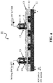
- FIG. 4 shows a magnetic device 10 according to an embodiment of the invention, for a memory device application.
- the magnetic device 10 of FIG. 4 is a magnetic DW racetrack memory device.
- the magnetic device 10 includes the seed layer 11; the first free magnetic layer 12 provided on the seed layer; the interlayer 13 provided on the first free magnetic layer 12; the second free magnetic layer 14 provided on the interlayer 13, wherein the first free magnetic layer 12 and the second free magnetic layer 14 are ferromagnetically coupled across the interlayer 13 through exchange interaction; the tunnel barrier 15 provided on the second free magnetic layer 14; and the fixed magnetic layer 16.
- the magnetic device 10 of FIG. 4 two exposed layer stacks, or pillars, are structured from the fixed magnetic layer 16, the tunnel barrier 15, and the second free magnetic layer 14.
- the interlayer 13, the first free magnetic layer 12 and the seed layer 11 are continuous between the two exposed layer stacks, as explained above.
- the magnetic device 10 further comprises four terminals, two of which are connected to the seed layer 11, and one terminal is connected to each pillar.
- writing into the second free magnetic layer 14 can be achieved by STT effect, via the terminal connected to one of the pillars, whereas DW motion in induced by means of SOT, via the two terminals connected to the seed layer 11.
- This may be supported by a high SOT efficiency layer as the seed layer 11, such as Pt, Ta, W or Hf or a topological insulator layer with strong SOC.
- Reading from the second free magnetic layer 14 can be carried out by means of TMR, via the terminal connected to the second (or output) pillar.
- the terminals may also comprise an electrode provided on the pillars and/or on the seed layer 11.
- the magnetic device 10 of FIG. 4 enables a DW conduit for high DW speed which is also robust to etching process. Furthermore, it alleviates device integration challenges and enhances DW transport performance.
- FIG. 2 and FIG. 4 show two extremes in the etch window that can be used for etching the pillars.
- the etch of the pillars is stopped at the tunnel barrier 15 as desired in the conventional device 70.
- damage to the tunnel barrier 15 in the inter-pillar space of the magnetic device 10 does not influence PMA in the shared first free magnetic layer 12 and, hence, does not affect DW transport.
- FIG. 4 shows in this respect that the pillar etch is stopped only at the interlayer 13, which is insensitive to etching, without affecting the DW transport. This is a major advantage of the magnetic device 10 and its manufacturing method over the conventional magnetic device 70 and its manufacturing method.
- the etching of the pillar, and the potential negative influences described in the background with respect to FIG. 8A and FIG. 8B are not critical anymore. If the etching goes too deep and destroys the magnetization of the second free magnetic layer 14 this is not a problem, as the first free magnetic layer 12 magnetization will not be influenced.
- FIG. 5 shows a magnetic device 10 according to an embodiment of the invention, for DW logic device applications, in particular the magnetic device 10 may be a spin torque majority gate device.
- the magnetic device 10 comprises four exposed layer stacks, or pillars, which are structured from the fixed magnetic layer 16, the tunnel barrier 15, and the second free magnetic layer 14. Three of the pillars may be regarded as input pillars, whereas the fourth pillar can be considered as an output.
- the interlayer 13, the first free magnetic layer 12, and the seed layer 11 are continuous between the exposed layer stacks and therefore are shared by the four separated pillars.
- the magnetic device 10 comprises the first free magnetic layer 12 provided on the seed layer 11; the interlayer 13 provided on the first free magnetic layer 12; the second free magnetic layer 14 provided on the interlayer 13, wherein the first 12 and the second 14 free magnetic layers are ferromagnetically coupled across the interlayer 13 through exchange interaction; the tunnel barrier 15 provided on the second free magnetic layer 14; and the fixed magnetic layer 16 provided on the tunnel barrier 15, as described above with respect to FIG. 1 .
- the magnetic device 10 of FIG. 5 further comprises several terminals. Especially in this example, three terminals are connected to the seed layer 11 and one terminal is connected to each exposed layer stack or pillar. Further, the terminals shown in FIG. 5 also comprise each an electrode.
- DW writing into the second free magnetic layer 14 can be carried out by means of STT (e.g. via one terminal connected to each input pillar, particularly to the fixed layer 16 of each pillar).
- DW reading can be carried out by TMR at the output pillar (e.g. via another terminal connected to the fixed layer 16 of said output pillar).
- DW transport can be achieved via the shared first free magnetic layer 12, driven by a SOT effect of the seed layer 11.
- the terminals connected to the seed layer 11 may be used.
- the seed layer 11 may thus be a SOT generating layer, for instance, a Pt, Ta, W or Hf, or a topological insulator layer with high SOC.
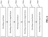
- FIG. 6 shows a schematic representation of an embodiment for a method according to the second aspect of the invention.
- the method comprises processing steps for manufacturing the magnetic device 10 as disclosed above.
- the method may comprise the steps of: providing S101 a seed layer; providing S102 a first free magnetic layer on the seed layer; providing S103 an interlayer on the first free magnetic layer; providing S104 a second free magnetic layer on the interlayer, wherein the first free magnetic layer and the second free magnetic layer are ferromagnetically coupled across the interlayer through exchange interaction; providing S105 a tunnel barrier on the second free magnetic layer; and providing S106 a fixed magnetic layer.
- the foregoing steps are not necessarily implemented in the indicated order.
- the method steps relate to the relative position of the layers of the material stack, which depends on the fabrication/growth direction of the layers.
- said method steps must be understood in a reverse order.
- the method may further comprise the step of structuring two or more exposed layer stacks, in particular two or more pillars, comprising one of: the fixed magnetic layer; the fixed magnetic layer and the tunnel barrier; or the fixed magnetic layer, the tunnel barrier, and the first free magnetic layer.
- the step of providing four or more terminals, wherein two terminals are connected to the seed layer, and wherein one terminal is connected to each exposed layer stack may also be comprised.
- the method may be further developed to fabricate further features of the magnetic device 10, as described above. Hence, the method achieves the same advantages as the magnetic device 10.
Landscapes
- Engineering & Computer Science (AREA)
- Chemical & Material Sciences (AREA)
- Crystallography & Structural Chemistry (AREA)
- Power Engineering (AREA)
- Physics & Mathematics (AREA)
- Computer Hardware Design (AREA)
- Manufacturing & Machinery (AREA)
- Condensed Matter Physics & Semiconductors (AREA)
- General Physics & Mathematics (AREA)
- Hall/Mr Elements (AREA)
- Mram Or Spin Memory Techniques (AREA)
Priority Applications (2)
| Application Number | Priority Date | Filing Date | Title |
|---|---|---|---|
| EP19201001.5A EP3800643A1 (de) | 2019-10-02 | 2019-10-02 | Magnetische vorrichtung mit einem hybriden freien schichtstapel |
| US17/038,470 US11587708B2 (en) | 2019-10-02 | 2020-09-30 | Magnetic device with a hybrid free layer stack |
Applications Claiming Priority (1)
| Application Number | Priority Date | Filing Date | Title |
|---|---|---|---|
| EP19201001.5A EP3800643A1 (de) | 2019-10-02 | 2019-10-02 | Magnetische vorrichtung mit einem hybriden freien schichtstapel |
Publications (1)
| Publication Number | Publication Date |
|---|---|
| EP3800643A1 true EP3800643A1 (de) | 2021-04-07 |
Family
ID=68136204
Family Applications (1)
| Application Number | Title | Priority Date | Filing Date |
|---|---|---|---|
| EP19201001.5A Pending EP3800643A1 (de) | 2019-10-02 | 2019-10-02 | Magnetische vorrichtung mit einem hybriden freien schichtstapel |
Country Status (2)
| Country | Link |
|---|---|
| US (1) | US11587708B2 (de) |
| EP (1) | EP3800643A1 (de) |
Families Citing this family (14)
| Publication number | Priority date | Publication date | Assignee | Title |
|---|---|---|---|---|
| EP2449561A2 (de) | 2009-06-30 | 2012-05-09 | Plextronics, Inc. | Polymere mit mindestens einer bithiophen-wiederholeinheit, syntheseverfahren für diese polymere und zusammensetzungen damit |
| US8691931B2 (en) | 2009-09-04 | 2014-04-08 | Plextronics, Inc. | Organic electronic devices and polymers, including photovoltaic cells and diketone-based and diketopyrrolopyrrole-based polymers |
| KR101797783B1 (ko) | 2009-09-29 | 2017-11-14 | 솔베이 유에스에이 인크. | 유기 전자 소자, 조성물 및 방법 |
| US9062152B2 (en) | 2010-09-01 | 2015-06-23 | Solvay Usa, Inc. | Organic electronic devices, including organic photovoltaic devices, polymers, and monomers |
| WO2012082893A2 (en) | 2010-12-15 | 2012-06-21 | Plextronics, Inc. | Fluoro monomers, oligomers, and polymers for inks and organic electronic devices |
| US11362269B2 (en) * | 2019-08-16 | 2022-06-14 | National University Of Singapore | Spin-orbit torque device and method for operating a spin-orbit torque device |
| KR102284925B1 (ko) * | 2020-05-07 | 2021-08-03 | 한국과학기술원 | 자기 로직 소자 |
| DE102020114551B4 (de) * | 2020-05-29 | 2024-10-24 | Infineon Technologies Ag | Magnetoresistiver Sensor und Fertigungsverfahren für einen magnetoresistiven Sensor |
| US11763973B2 (en) * | 2021-08-13 | 2023-09-19 | Western Digital Technologies, Inc. | Buffer layers and interlayers that promote BiSbx (012) alloy orientation for SOT and MRAM devices |
| US11532323B1 (en) * | 2021-08-18 | 2022-12-20 | Western Digital Technologies, Inc. | BiSbX (012) layers having increased operating temperatures for SOT and MRAM devices |
| EP4177892B1 (de) * | 2021-11-03 | 2024-09-11 | Imec VZW | Speichervorrichtung basierend auf einer magnetischen domänenwand mit spurkreuzender architektur |
| US12081213B1 (en) * | 2022-05-31 | 2024-09-03 | Ceremorphic, Inc. | System and method for skyrmion based logic device |
| EP4307872A1 (de) * | 2022-07-13 | 2024-01-17 | Imec VZW | Chiral schaltende, angetriebene spin-torque-logikgatter |
| US12212316B1 (en) * | 2022-07-31 | 2025-01-28 | Ceremorphic, Inc. | System and method for synthetic antiferromagnet skyrmion based logic device |
Citations (1)
| Publication number | Priority date | Publication date | Assignee | Title |
|---|---|---|---|---|
| US20170179373A1 (en) | 2015-12-21 | 2017-06-22 | Imec Vzw | Spin torque majority gate device |
Family Cites Families (9)
| Publication number | Priority date | Publication date | Assignee | Title |
|---|---|---|---|---|
| KR101549625B1 (ko) * | 2014-04-18 | 2015-09-04 | 한양대학교 산학협력단 | 메모리 소자 |
| KR101583783B1 (ko) * | 2014-04-18 | 2016-01-13 | 한양대학교 산학협력단 | 메모리 소자 |
| US10580964B2 (en) * | 2015-03-18 | 2020-03-03 | Industry-University Cooperation Foundation Hanyang University | Memory device |
| CN109155360A (zh) * | 2016-02-05 | 2019-01-04 | 汉阳大学校产学协力团 | 存储器件 |
| KR102169622B1 (ko) * | 2018-01-17 | 2020-10-26 | 한양대학교 산학협력단 | 메모리 소자 |
| US11152047B2 (en) * | 2019-10-23 | 2021-10-19 | Western Digital Technologies, Inc. | Magnetoresistive random access memory containing multilayer synthetic antiferromagnetic structure and method of making thereof |
| US11289143B2 (en) * | 2019-10-30 | 2022-03-29 | Taiwan Semiconductor Manufacturing Co., Ltd. | SOT-MRAM with shared selector |
| EP3961632A1 (de) * | 2020-08-25 | 2022-03-02 | Commissariat à l'Energie Atomique et aux Energies Alternatives | Magnetischer tunnelübergang mit einer inhomogenen granulären freien schicht und zugehörige spintronikvorrichtungen |
| US11474167B1 (en) * | 2021-08-13 | 2022-10-18 | National University Of Singapore | Method and an apparatus for detecting a magnetic field |
-
2019
- 2019-10-02 EP EP19201001.5A patent/EP3800643A1/de active Pending
-
2020
- 2020-09-30 US US17/038,470 patent/US11587708B2/en active Active
Patent Citations (1)
| Publication number | Priority date | Publication date | Assignee | Title |
|---|---|---|---|---|
| US20170179373A1 (en) | 2015-12-21 | 2017-06-22 | Imec Vzw | Spin torque majority gate device |
Non-Patent Citations (7)
| Title |
|---|
| AJEJAS ET AL.: "Tuning domain wall velocity with Dzyaloshinskii-Moriya interaction", APPL. PHYS. LETT., vol. 111, no. 20, 2017, pages 202402, XP012223611, doi:10.1063/1.5005798 |
| CARETTA ET AL.: "Fast current-driven domain walls and small skyrmions in a compensated ferrimagnet", NATURE NANOTECHNOLOGY, vol. 13, 2018, pages 1154 - 1160, XP036653487, doi:10.1038/s41565-018-0255-3 |
| JIN-YOUNG CHOI ET AL: "Double Pinned Perpendicular-Magnetic-Tunnel-Junction Spin-Valve Providing Multi-level Resistance States", SCIENTIFIC REPORTS, vol. 9, no. 1, 15 August 2019 (2019-08-15), XP055687149, DOI: 10.1038/s41598-019-48311-0 * |
| MENG HAO ET AL: "Composite free layer for high density magnetic random access memory with lower spin transfer current", APPLIED PHYSICS LETTERS, AMERICAN INSTITUTE OF PHYSICS, 2 HUNTINGTON QUADRANGLE, MELVILLE, NY 11747, vol. 89, no. 15, 12 October 2006 (2006-10-12), pages 152509 - 152509, XP012086310, ISSN: 0003-6951, DOI: 10.1063/1.2361280 * |
| MIRON ET AL.: "Fast current-induced domain-wall motion controlled by the Rashba effect", NATURE MATERIALS, vol. 10, 2011, pages 419 - 423 |
| PARKIN ET AL.: "Memory on the racetrack", NATURE NANOTECHNOLOGY, vol. 10, March 2015 (2015-03-01), pages 195 |
| YANG ET AL.: "Domain-wall velocities of up to 750 m s-1 driven by exchange-coupling torque in synthetic antiferromagnets", NATURE NANOTECHNOLOGY, vol. 10, 2015, pages 221 - 226 |
Also Published As
| Publication number | Publication date |
|---|---|
| US20210104344A1 (en) | 2021-04-08 |
| US11587708B2 (en) | 2023-02-21 |
Similar Documents
| Publication | Publication Date | Title |
|---|---|---|
| US11587708B2 (en) | Magnetic device with a hybrid free layer stack | |
| US11823736B1 (en) | Superconducting devices with ferromagnetic barrier junctions | |
| CN111834521B (zh) | 磁性隧道结器件 | |
| TWI783018B (zh) | 半導體結構以及相關操作和製造方法 | |
| CN106374035B (zh) | 使用外部铁磁偏置膜的压控磁各向异性切换装置 | |
| KR100851689B1 (ko) | 자성 부재 및 자성 부재를 제공하는 방법 | |
| US7602000B2 (en) | Spin-current switched magnetic memory element suitable for circuit integration and method of fabricating the memory element | |
| US9666793B2 (en) | Method of manufacturing magnetoresistive element(s) | |
| EP1745488B1 (de) | Mit spin-dämmung erweitertes element mit magnetoresistiver wirkung und dieses verwendender magnetspeicher | |
| US8482968B2 (en) | Non-volatile magnetic tunnel junction transistor | |
| CN101067967B (zh) | 磁性存储装置 | |
| US20140008742A1 (en) | Magnetic tunneling junction seed, capping, and spacer layer materials | |
| CN108376736A (zh) | 磁装置和用于设置磁装置的方法 | |
| CN105244436A (zh) | 使用不对称的自由层且适用于自旋转移矩存储器的磁性结 | |
| US20140217487A1 (en) | Stt-mram and method of manufacturing the same | |
| US9741929B2 (en) | Method of making a spin-transfer-torque magnetoresistive random access memory (STT-MRAM) | |
| US20180269384A1 (en) | Method and system for providing a dual magnetic junction having mitigated flowering field effects | |
| US12096700B2 (en) | Spintronic device with synthetic antiferromagnet hybrid storage layer | |
| TWI643367B (zh) | 形成磁性裝置的自由層的材料組成、自由層與磁性元件 | |
| KR20250113518A (ko) | 자기 저항 효과 소자 및 자기 메모리 | |
| US10374147B2 (en) | Perpendicular magnetic tunnel junction having improved reference layer stability | |
| Makarov et al. | Field-free fast reliable deterministic switching in perpendicular spin-orbit torque MRAM cells | |
| Nagase et al. | Progress and challenges towards high-density magnetic random access memory: evolution of high-performance perpendicularly magnetized magnetic tunnel junctions with elaborate cell structure design | |
| CN118574501A (zh) | 电压控制磁各向异性的磁性隧道结 |
Legal Events
| Date | Code | Title | Description |
|---|---|---|---|
| PUAI | Public reference made under article 153(3) epc to a published international application that has entered the european phase |
Free format text: ORIGINAL CODE: 0009012 |
|
| STAA | Information on the status of an ep patent application or granted ep patent |
Free format text: STATUS: THE APPLICATION HAS BEEN PUBLISHED |
|
| AK | Designated contracting states |
Kind code of ref document: A1 Designated state(s): AL AT BE BG CH CY CZ DE DK EE ES FI FR GB GR HR HU IE IS IT LI LT LU LV MC MK MT NL NO PL PT RO RS SE SI SK SM TR |
|
| AX | Request for extension of the european patent |
Extension state: BA ME |
|
| STAA | Information on the status of an ep patent application or granted ep patent |
Free format text: STATUS: REQUEST FOR EXAMINATION WAS MADE |
|
| 17P | Request for examination filed |
Effective date: 20211005 |
|
| RBV | Designated contracting states (corrected) |
Designated state(s): AL AT BE BG CH CY CZ DE DK EE ES FI FR GB GR HR HU IE IS IT LI LT LU LV MC MK MT NL NO PL PT RO RS SE SI SK SM TR |
|
| RAP3 | Party data changed (applicant data changed or rights of an application transferred) |
Owner name: KATHOLIEKE UNIVERSITEIT LEUVEN Owner name: IMEC VZW |
|
| STAA | Information on the status of an ep patent application or granted ep patent |
Free format text: STATUS: EXAMINATION IS IN PROGRESS |
|
| 17Q | First examination report despatched |
Effective date: 20240110 |
|
| RAP3 | Party data changed (applicant data changed or rights of an application transferred) |
Owner name: KATHOLIEKE UNIVERSITEIT LEUVEN Owner name: IMEC VZW |