EP3806084A1 - Anzeigevorrichtung, verfahren zur automatischen anpassung der helligkeit eines bildschirms und endgeräteausrüstung - Google Patents
Anzeigevorrichtung, verfahren zur automatischen anpassung der helligkeit eines bildschirms und endgeräteausrüstung Download PDFInfo
- Publication number
- EP3806084A1 EP3806084A1 EP19750046.5A EP19750046A EP3806084A1 EP 3806084 A1 EP3806084 A1 EP 3806084A1 EP 19750046 A EP19750046 A EP 19750046A EP 3806084 A1 EP3806084 A1 EP 3806084A1
- Authority
- EP
- European Patent Office
- Prior art keywords
- light
- display
- layer
- photoelectric sensor
- ambient light
- Prior art date
- Legal status (The legal status is an assumption and is not a legal conclusion. Google has not performed a legal analysis and makes no representation as to the accuracy of the status listed.)
- Pending
Links
Images


Classifications
-
- G—PHYSICS
- G09—EDUCATION; CRYPTOGRAPHY; DISPLAY; ADVERTISING; SEALS
- G09G—ARRANGEMENTS OR CIRCUITS FOR CONTROL OF INDICATING DEVICES USING STATIC MEANS TO PRESENT VARIABLE INFORMATION
- G09G3/00—Control arrangements or circuits, of interest only in connection with visual indicators other than cathode-ray tubes
- G09G3/20—Control arrangements or circuits, of interest only in connection with visual indicators other than cathode-ray tubes for presentation of an assembly of a number of characters, e.g. a page, by composing the assembly by combination of individual elements arranged in a matrix no fixed position being assigned to or needed to be assigned to the individual characters or partial characters
- G09G3/22—Control arrangements or circuits, of interest only in connection with visual indicators other than cathode-ray tubes for presentation of an assembly of a number of characters, e.g. a page, by composing the assembly by combination of individual elements arranged in a matrix no fixed position being assigned to or needed to be assigned to the individual characters or partial characters using controlled light sources
- G09G3/30—Control arrangements or circuits, of interest only in connection with visual indicators other than cathode-ray tubes for presentation of an assembly of a number of characters, e.g. a page, by composing the assembly by combination of individual elements arranged in a matrix no fixed position being assigned to or needed to be assigned to the individual characters or partial characters using controlled light sources using electroluminescent panels
- G09G3/32—Control arrangements or circuits, of interest only in connection with visual indicators other than cathode-ray tubes for presentation of an assembly of a number of characters, e.g. a page, by composing the assembly by combination of individual elements arranged in a matrix no fixed position being assigned to or needed to be assigned to the individual characters or partial characters using controlled light sources using electroluminescent panels semiconductive, e.g. using light-emitting diodes [LED]
- G09G3/3208—Control arrangements or circuits, of interest only in connection with visual indicators other than cathode-ray tubes for presentation of an assembly of a number of characters, e.g. a page, by composing the assembly by combination of individual elements arranged in a matrix no fixed position being assigned to or needed to be assigned to the individual characters or partial characters using controlled light sources using electroluminescent panels semiconductive, e.g. using light-emitting diodes [LED] organic, e.g. using organic light-emitting diodes [OLED]
-
- G—PHYSICS
- G09—EDUCATION; CRYPTOGRAPHY; DISPLAY; ADVERTISING; SEALS
- G09G—ARRANGEMENTS OR CIRCUITS FOR CONTROL OF INDICATING DEVICES USING STATIC MEANS TO PRESENT VARIABLE INFORMATION
- G09G5/00—Control arrangements or circuits for visual indicators common to cathode-ray tube indicators and other visual indicators
- G09G5/10—Intensity circuits
-
- H—ELECTRICITY
- H10—SEMICONDUCTOR DEVICES; ELECTRIC SOLID-STATE DEVICES NOT OTHERWISE PROVIDED FOR
- H10K—ORGANIC ELECTRIC SOLID-STATE DEVICES
- H10K59/00—Integrated devices, or assemblies of multiple devices, comprising at least one organic light-emitting element covered by group H10K50/00
- H10K59/10—OLED displays
- H10K59/12—Active-matrix OLED [AMOLED] displays
- H10K59/126—Shielding, e.g. light-blocking means over the TFTs
-
- H—ELECTRICITY
- H10—SEMICONDUCTOR DEVICES; ELECTRIC SOLID-STATE DEVICES NOT OTHERWISE PROVIDED FOR
- H10K—ORGANIC ELECTRIC SOLID-STATE DEVICES
- H10K59/00—Integrated devices, or assemblies of multiple devices, comprising at least one organic light-emitting element covered by group H10K50/00
- H10K59/60—OLEDs integrated with inorganic light-sensitive elements, e.g. with inorganic solar cells or inorganic photodiodes
-
- G—PHYSICS
- G09—EDUCATION; CRYPTOGRAPHY; DISPLAY; ADVERTISING; SEALS
- G09G—ARRANGEMENTS OR CIRCUITS FOR CONTROL OF INDICATING DEVICES USING STATIC MEANS TO PRESENT VARIABLE INFORMATION
- G09G2320/00—Control of display operating conditions
- G09G2320/06—Adjustment of display parameters
- G09G2320/0626—Adjustment of display parameters for control of overall brightness
-
- G—PHYSICS
- G09—EDUCATION; CRYPTOGRAPHY; DISPLAY; ADVERTISING; SEALS
- G09G—ARRANGEMENTS OR CIRCUITS FOR CONTROL OF INDICATING DEVICES USING STATIC MEANS TO PRESENT VARIABLE INFORMATION
- G09G2360/00—Aspects of the architecture of display systems
- G09G2360/14—Detecting light within display terminals, e.g. using a single or a plurality of photosensors
- G09G2360/141—Detecting light within display terminals, e.g. using a single or a plurality of photosensors the light conveying information used for selecting or modulating the light emitting or modulating element
-
- G—PHYSICS
- G09—EDUCATION; CRYPTOGRAPHY; DISPLAY; ADVERTISING; SEALS
- G09G—ARRANGEMENTS OR CIRCUITS FOR CONTROL OF INDICATING DEVICES USING STATIC MEANS TO PRESENT VARIABLE INFORMATION
- G09G2360/00—Aspects of the architecture of display systems
- G09G2360/14—Detecting light within display terminals, e.g. using a single or a plurality of photosensors
- G09G2360/144—Detecting light within display terminals, e.g. using a single or a plurality of photosensors the light being ambient light
-
- G—PHYSICS
- G09—EDUCATION; CRYPTOGRAPHY; DISPLAY; ADVERTISING; SEALS
- G09G—ARRANGEMENTS OR CIRCUITS FOR CONTROL OF INDICATING DEVICES USING STATIC MEANS TO PRESENT VARIABLE INFORMATION
- G09G2360/00—Aspects of the architecture of display systems
- G09G2360/14—Detecting light within display terminals, e.g. using a single or a plurality of photosensors
- G09G2360/145—Detecting light within display terminals, e.g. using a single or a plurality of photosensors the light originating from the display screen
- G09G2360/147—Detecting light within display terminals, e.g. using a single or a plurality of photosensors the light originating from the display screen the originated light output being determined for each pixel
-
- H—ELECTRICITY
- H10—SEMICONDUCTOR DEVICES; ELECTRIC SOLID-STATE DEVICES NOT OTHERWISE PROVIDED FOR
- H10K—ORGANIC ELECTRIC SOLID-STATE DEVICES
- H10K59/00—Integrated devices, or assemblies of multiple devices, comprising at least one organic light-emitting element covered by group H10K50/00
- H10K59/10—OLED displays
- H10K59/12—Active-matrix OLED [AMOLED] displays
- H10K59/13—Active-matrix OLED [AMOLED] displays comprising photosensors that control luminance
Definitions
- Embodiments of the present disclosure relate to a display device, a method of automatically adjusting brightness of a display screen of the display device and a terminal equipment for carrying out the method of automatically adjusting brightness of the display screen of the display device.
- An ambient light detection device is usually arranged in a View area (that is, VA) or a black matrix (BM) area of a display panel, where the BM area usually refers to a non-display area, that is, an AA area, a border region outside of an operable region.
- the ambient light detection device needs to additionally occupy a corresponding region of the display panel, which is adverse to the realization of a borderless screen.
- An embodiment of the present disclosure provides a display device, an ambient light detection device is integrated in a visible area of the display device, which is advantage to the realization of bezel-less of display screen.
- An embodiment of the present disclosure also provides a method of automatically adjusting brightness of a display screen of the display device.
- An embodiment of the present disclosure also provides a terminal equipment for carrying out the method of automatically adjusting brightness of the display screen of the display device.
- At least one embodiment of the present disclosure provides a display device, comprising an ambient light detection device including a light blocking layer and a photoelectric sensor, a display assembly, and a control device.
- the display assembly comprises a backpanel assembly, the light blocking layer being arranged in the backpanel assembly and provided with a light passing hole suitable for the passing of ambient light, the photoelectric sensor being arranged under the backpanel assembly and configured to detect the variance of the ambient light; a display screen provided over the backpanel assembly; a display chip connected with the display screen.
- the control device is connected with the photoelectric sensor to receive and process an optical signal sensed by the photoelectric sensor, and the display chip is connected with the control device, to adjust brightness of the display screen according to variance of the ambient light.
- the backpanel assembly comprises: a substrate, the light blocking layer being disposed on an upper surface of the substrate, and the photoelectric sensor being disposed under the substrate; a light-emitting layer above the light blocking layer; an anode on a lower surface of the light-emitting layer; and a cathode on an upper surface of the light-emitting layer.
- the light passing hole is configured to allow light emitted by the light-emitting layer not to travel toward the photoelectric sensor via the light passing hole after they are reflected by the cathode, to eliminate interference of light emitted by the light-emitting layer to the ambient light.
- a vertical line perpendicular to a plane where the light blocking layer is located is drawn to go through an intersection of the reflected light and the light blocking layer, and an included angle between the vertical line and the reflected light is greater than about 30°.
- the backpanel further comprises: a back film on a lower surface of the substrate, the photoelectric sensor being disposed under the back film; and a thin film transistor layer between the light blocking layer and the anode.
- the ambient light detection device further comprises a low refractivity layer, the low refractivity layer being arranged between the photoelectric sensor and the substrate, and configured to allow the passing of the ambient light, and to allow light emitted by the light-emitting layer to be totally reflected when it travels toward the low refractivity layer.
- the low refractivity layer is a silicon dioxide layer, or the substrate and the photoelectric sensor is bonded and a cavity is defined between the bonded substrate and photoelectric sensor, and the low refractivity layer is an air layer.
- the light passing hole is a through hole that runs through the light blocking layer along a thickness direction, and the through hole is formed to be a circle hole or a polygon hole.
- a plurality of the light passing holes are provided and arranged in array, and the light passing holes have a maximum radial dimension of about 5 ⁇ m to about 15 ⁇ m.
- the light-emitting layer has a thickness about 1 ⁇ m or less.
- the display device further comprises a protective layer, a packaging layer, and a pixel definition layer.
- the protective layer is provided over the ambient light detection device
- the packaging layer is provided above the cathode layer
- the pixel definition layer is provided in a same layer as the anode layer.
- At least one embodiment of the present disclosure provides a method of automatically adjusting the display screen brightness of the display device, comprising: the photoelectric sensor sensing the ambient light, the control device receiving an optical signal sensed by the photoelectric sensor, and comparing the optical signal with a signal stored in the display chip; determining whether or not an irradiation intensity of the ambient light reaches an adjusting threshold; if yes, sending an adjusting signal from the control device to the display chip, adjusting the driving current of the display screen by the display chip to change brightness of the display screen, and continuing to sense the ambient light by the photoelectric sensor; and if no, returning to continue to sense the ambient light by the photoelectric sensor.
- At least one embodiment of the present disclosure also provides a terminal equipment, the terminal equipment being configured to carry out the method of adjusting brightness of the display screen of the display device, the terminal equipment comprises a photoelectric sensor, a display assembly and a control device. Both the photoelectric sensor and the display assembly are electrically connected to the control device, and the display assembly includes a display chip and a display screen.
- the photoelectric sensor is configured to sense ambient light and acquire an optical signal;
- the control device is configured to compare the optical signal sensed by the photoelectric sensor with a signal stored in the display chip, and to determine whether or not the irradiation intensity of the ambient light reaches an adjusting threshold, if yes, send an adjusting signal to the display chip;
- the display chip is configured to adjust a driving current of the display screen based on the adjusting signal, to change the brightness of the display screen.
- the photoelectric sensor is electrically connected to the control device by a sensor flexible circuit board
- the display assembly is electrically connected to the control device by a display flexible circuit board.
- connection/connecting/connected is not limited to a physical connection or mechanical connection, but may include an electrical connection/coupling, directly or indirectly.
- the terms, “on,” “under,” “left,” “right” or the like are only used to indicate relative position relationship, and when the position of the object which is described is changed, the relative position relationship may be changed accordingly.
- a display device 100 according to an embodiment of the present disclosure will be described below in conjunction with the accompanying drawings.
- an ambient light detection device 1 is integrated in an operable region of the display device 100.
- the occupation of a border region around the operable region by the ambient light detection device 1 can be decreased, and it is beneficial to the realization of non-bezel screen.
- an ambient light detection device 1 may include a light blocking layer 11 and a photoelectric sensor 12.
- the light blocking layer 11 may be a metal layer, such as a molybdenum layer, a titanium layer, a silver layer, etc., and the light blocking layer 11 has a thickness which can be set adaptively according to the actual needs.
- the display device 100 includes a display assembly 2 and a control device 3.
- the display assembly 2 includes a backpanel assembly 21, a display screen 22, and a display chip.
- the light blocking layer 11 of the ambient light detection device 1 may be arranged in the backpanel assembly 21.
- the backpanel assembly 21 has a multilayered structure, the light blocking layer 11 belongs to one layer in the multilayered structure; and in the light blocking layer 11, a light passing hole 111 is provided which is suitable for allowing the transmission of ambient light 4.
- a light passing hole 111 is provided which is suitable for allowing the transmission of ambient light 4.
- the display screen 22 is disposed on the backpanel assembly 21, the display chip is connected to the display screen 22, and the disposing position of the display chip can be selected.
- the photoelectric sensor 12 is disposed under the backpanel assembly 21 and configured to detect the variance of ambient light 4, and the variance here refers, for example, to a change in the photocurrent of a sensor caused by the ambient light illuminance.
- the control device 3 is connected to the photoelectric sensor 12 for receiving and processing an optical signal sensed by the photoelectric sensor 12, and the display chip is coupled to the control device 3, to adjust brightness of the display screen 22 according to variance of ambient light 4.
- the ambient light detection device 1 into the operable region of the display device 100, it is beneficial to reducing occupation of other regions of the display device 100 by the ambient light detection device 1, which contributes to realization of full screen display.
- control device 3 can receive and process an optical signal sensed by the photoelectric sensor 12, and compare the optical signal with an signal stored in the display chip, so that the display chip can adjust brightness of the display screen 22 based on the variance of the ambient light 4. In this way, not only power can be saved, but also the usage comfort of users is improved.
- control device 3 generally includes a Digital Signal Processing chip (DSP), a Printed Circuit Board (PCB), a Central Processing Unit (CPU), a display Integrated Chip (IC).
- DSP Digital Signal Processing chip
- PCB Printed Circuit Board
- CPU Central Processing Unit
- IC display Integrated Chip
- a photoelectric sensor senses an ambient light signal, and the ambient light signal is processed by the DSP (here, which is usually an interpolation fuzzification processing).
- the processed data is sent to a CPU by PCB, it is determined by the CPU whether or not brightness (or grayscale) of a display screen needs to be adjusted. If it does not reach a threshold, no adjustment is performed, and the operation is interrupted. If it reaches the threshold, adjustment is performed, an adjusting proportion is calculated, and the adjusting data is sent to a display integrated chip (IC).
- the adjusting data and DATA of the display data are stacked, and then it is sent to the display screen for display.
- the process may further include that, a grayscale control signal and the display raw data (RAW DATA) are coupled, and the final display data is transmitted to be displayed.
- DSP acts as a digital signal processing chip, which may be contained in a CMOS.
- the DSP framework includes an ISP (a signal processor).
- the DSP framework may further include a JPEG encoder (an image decoder).
- JPEG encoder an image decoder
- the display device 100 of the embodiment of the present disclosure by integrating the ambient light detection device 1 into an operable region of the display device 100, it is beneficial to saving the screen space and improving the screen-to-body ratio, as compared with the prior art. Furthermore, by coupling the control device 3 to the photoelectric sensor 12 and the display chip, respectively, the display device 100 can adjust brightness of the display screen 22 based on the variance of the ambient light 4, and the comfort for the user usage can be improved and energy is saved.
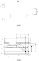
- the backpanel assembly 21 includes a substrate 211, a light-emitting layer 212, an anode 213 and a cathode 214.
- the light blocking layer 11 is arranged on an upper surface of the substrate 211, and the photoelectric sensor 12 for detecting the variance of ambient light 4 is arranged under the substrate 211; the light-emitting layer 212 is arranged above the light blocking layer 11; the anode 213 is arranged on a lower surface of the light-emitting layer 212; and the cathode 214 (e.g., a metal cathode) is arranged on an upper surface of the light-emitting layer 212.
- the cathode 214 e.g., a metal cathode
- the light-emitting layer 212 may be an organic Emitting Layer (that is, EL), and a light passing hole 111 is so configured that light emitted by the light-emitting layer 212 will not be exited to the photoelectric sensor 12 via the light passing hole 11 after they are reflected by the cathode 214, so as to eliminate the interference of the light emitted by the light-emitting layer 212 to the ambient light 4. In this way, it is beneficial to avoiding the interference of the light emitted by the light-emitting layer 212 itself to the ambient light 4, and this makes the detection of ambient light be accurate.
- EL organic Emitting Layer
- the light blocking layer 11 may block part of light, and for example, the light blocking layer 11 may block light emitted by the light-emitting layer 212, helping to reduce the interference of light emitted by the light-emitting layer 212 to the ambient light 4, and to improve the detective accuracy of the photoelectric sensor 12.
- brightness of the display screen 22 is adaptively adjusted by the display chip.
- the light passing hole 111 is a through hole running through the light blocking layer 11 along the thickness direction, and the through hole is configured into a circle or polygon. In this way, it helps to increase the transmittance, and the interference of light emitted by the light-emitting layer 212 to the ambient light 4 can also be avoided. This makes the detection of ambient light be accurate.
- a plurality of light passing holes 111 are provided, and the plurality of light passing holes 111 may be arranged in array. In this way, it is more beneficial to increasing the transmittance, and it also helps to avoid the interference of the light emitted by the light-emitting layer 212 itself to the ambient light 4. This makes the detection of the ambient light be accurate, and the brightness of the screen can be adjusted better.
- density of the light passing holes 111 may be increased as much as possible. For example, it is possible that a light passing hole 111 is made beside each of subpixels.
- the ambient light detection device 1 By designing the ambient light detection device 1 to rest in an operable region, the area of the display screen 22 can be increased, and a larger screen-to-body ratio can be achieved.
- the operable region may be disposed in a display region.
- a hole array may be formed on the full screen, and a hole or hole array may also be formed in some region of the screen. If it is made on the full screen, the whole screen may be called as an operating region. If it is only made in some region, owing to the fact that a sensor is relatively small, the sensor needs to be placed in a region where a hole array has been made. In this way, this partial region may be called as an operable region.
- the ambient light detection device 1 by integrating the ambient light detection device 1 into an operable region and automatically adjusting the screen brightness according to the ambient light, extra space can be saved.
- the screen area is increased, and the screen-to-body ratio is raised, which is beneficial to the realization of full screen display.
- the light blocking layer 11 and forming the light passing hole 111 in the light blocking layer 11, the interference of the light by the light-emitting layer 212 itself to the photoelectric sensor 12 for detecting the ambient light 4 is avoided. This makes the detection of ambient light be accurate, and a full-screen fingerprint identification can be realized. It is understandable that, regarding the process of fingerprint identification, reference may be made to a conventional fingerprint identification ways, and no description is repeated here.
- the maximum radial dimension of a light passing hole 111 is about 5 ⁇ m to about 15 ⁇ m.
- the maximum radial dimension of the light passing hole 111 is about 5 ⁇ m to about 15 ⁇ m.
- the maximum radial dimension of a light passing hole 111 may be, for example, about 5 ⁇ m, about 8 ⁇ m, about 10 ⁇ m, or about 15 ⁇ m, etc.
- the maximum radial dimension of the light passing hole 111 refers to diameter of the circular hole; when a light passing hole 111 is a polygonal hole, the maximum radial dimension of the light passing hole 111 refers to diameter of a circumcircle of the light passing hole 111, and the minimum radial dimension of the light passing hole 111 refers to diameter of an inscribed circle of the light passing hole 111, which are understandable to those skilled in the art.
- the thickness of the light-emitting layer 212 may be 1 ⁇ m or less.
- structure of the display device 100 is lighter, thinner and more compact.
- the display device 100 further includes a protective layer 5 (such as a protective glass cover, etc.), a packaging layer 6, and a pixel definition layer 7.
- a protective layer 5 such as a protective glass cover, etc.
- the protective layer 5 may be disposed on the outermost side of the display screen, and the display screen and the ambient light detection device 1 can be protected by the protective layer 5 in some extent. This helps to allow the accuracy of detection of the ambient light, and to prolong the service life of the display device 100.
- the packaging layer 6 may be disposed on the cathode 214, and the pixel definition layer 7 and the anode 213 may be arranged in a same layer.
- the display device may further include a polarizer 23 and a touch screen 24.
- the touch screen 24 may be bonded to the packaging layer 6 by an optical adhesive.
- the protective layer 5 may be arranged on the polarizer 23.
- the backpanel assembly 21 further includes a back film 215 and a thin film transistor layer 216, the back film 215 is disposed on a lower surface of the substrate 211, and a photoelectric sensor 12 is disposed under the back film 215.
- the back film 215 may be made of glass, or thermoplastic polyester PET (Polythylene terephthalate), etc.
- the thin film transistor layer 216 may be arranged between the light blocking layer 11 and the anode 213.
- the display chip is coupled with the thin film transistor layer 216, and the lightness and darkness of each pixel may be adjusted by the display chip.
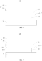
- a vertical line perpendicular to the plane where the light blocking layer 11 is located is drawn to go through an intersection of the reflected light and the light blocking layer 11, and an included angle between the vertical line and the reflected light is greater than about 30 degrees. This is more helpful for avoiding the interference of the light emitted by the light-emitting layer 212 itself to the ambient light 4, and so detection of ambient light is accurate.
- a light emitted by the light-emitting layer 212 has an intersection with the cathode 214 and is reflected to the light blocking layer 11 via the intersection.
- the projection of a light passing hole 111 on the light blocking layer 11 is a circle, and the light passing hole 111 has an end point at either end along the diameter direction.
- the intersection is connected with the end point so as to form a first connecting line, a vertical line perpendicular to the plane where the light blocking layer 11 is located is drawn to go through the end point so as to form a second connecting line, and an included angle between the first connecting line and the second connecting line is greater than about 30 degrees.
- one point at the margin of an upper surface of the light-emitting layer 212 is A1
- one point at the margin of a lower surface of the light-emitting layer 212 is A3
- one point at the margin that is situated somewhere between the upper surface and the lower surface of the light-emitting layer 212 is A2
- the end points includes a first end point B1 and a second end point B2.
- a vertical line that goes through the first end point B1 and is perpendicular to the plane where the light blocking layer 11 is located has a first intersection of O1 with the cathode 214, and the first included angle ⁇ A1B101 (or called as ⁇ 1 ) is greater than about 30 degrees.
- intersections further include a second intersection O2, a third intersection O3 and a fourth intersection O4.
- the second included angle ⁇ O2B1O1 (or called as ⁇ 2 ) is greater than about 30 degrees.
- a vertical line that goes through the second end point B2 has a fourth intersection of O4 with the cathode 214, and the third included angle ⁇ O3B2O4 (or called as ⁇ 3 ) is greater than about 30 degrees.
- the ambient light 4 enters the photoelectric sensor 12 through the light passing hole 111 for photosensing, and the photoelectric sensor 12 detects the photosensed energy that is integrated.
- the control device 3 is coupled with the photoelectric sensor 12 and the display chip, respectively, and determines the intensity of the ambient light 4, and the brightness of the display screen 22 is automatically adjusted by the display chip.
- the light passing hole 111 can play a role of shielding the display device 100, such as an internal light-emitting layer 212 of an OLED (Organic Light-Emitting Diode), from giving off light, so as to avoid stray lights inside the display device 100 interfere with the detection of the photoelectric sensor 12 and resulting in a misjudgment.
- OLED Organic Light-Emitting Diode
- ⁇ 1 arctan B E
- ⁇ 2 arctan B 2 E ⁇ F
- ⁇ 3 arctan B 2 E ⁇ F
- A denotes the vertical distance between a second light-emitting point and an intersection of a reflected light and a light blocking layer
- B denotes the vertical distance between a first light-emitting point and an intersection of a light or a reflected light and the light blocking layer
- E denotes the vertical distance between a lower surface of a reflective layer and an upper surface of the light blocking layer
- F denotes the vertical distance between a lower surface
- thickness of the light-emitting layer 212 shown in FIG. 3 to FIG. 5 is very thin, and for illustration, structure of the light-emitting layer 212 and a portion of light rays are schematically drawn in the figure.
- the ambient light detection device 1 may further include a low refractivity layer 13.
- the ambient light detection device 1 may further include a low refractivity layer 13 that is arranged between a photoelectric sensor 12 and a substrate 211.
- the low refractivity layer 13 is configured to allow the ambient light to pass through, and to allow the light emitted by a light-emitting layer 212 to be totally reflected when travelling to the low refractivity layer 13.
- a back film 215 is disposed on a lower surface of the substrate 211, and the low refractivity layer 13 may be arranged between the photoelectric sensor 12 and the back film 215.
- the low refractivity layer 13 may be a silicon dioxide layer, or a bonding layer between the substrate 211 and the photoelectric sensor 12.
- a cavity may be defined between the substrate 211 and the photoelectric sensor 12, and the low refractivity layer 13 may be an air layer.
- the form or material of low refractivity layer 13 may be selected as needed.
- the low refractivity layer 13 basically has no effect on the ambient light 4.
- the ambient light 4 can be transmitted through the low refractivity layer 13 and arrive at a surface of the photoelectric sensor 12, but the self-emissive light inside the display device 100 will also suffer internal reflection, majority of them will be blocked by the light blocking layer 11, and will not cause any interference. Even if part of light rays emitted by the light-emitting layer 212 is incident into the light passing hole 111 of the light blocking layer 11, their incident angles will be relatively big, and they are totally reflected by the low reflectivity layer 13, and will not reach the surface of the photoelectric sensor 12. In this way, those detected by the photoelectric sensor 12 are basically ambient light 4, and this can make the detection be accurate. As a result, brightness of the display screen 22 can be changed according to brightness variance of ambient light rays, and will not be affected by a display picture of the display device.
- FIG. 8 it is the light energy sensed by a photoelectric sensor 12 in an indoor bright state; as shown in FIG. 9 and FIG. 10 , they are the light energy sensed by the photoelectric sensor 12 in indoor slightly dark states; and as shown in FIG. 11 , it is the light energy sensed in an indoor light-off state. All of these tests are performed in a state of lighting screen (that is, a state that the display screen is lit up). It can be seen clearly that, with the change of ambient light 4, the light energy sensed by the photoelectric sensor 12 also changes with it, and no interference is produced to the ambient light 4 in the state that the display screen is lit up.
- a method of automatically adjusting the display screen brightness of the above display device is also provided.
- the photoelectric sensor senses the ambient light
- the control device receives an optical signal sensed by the photoelectric sensor, and compares the optical signal with a signal stored in the display chip.
- the control device determines whether or not the irradiation intensity of the ambient light reaches an adjusting threshold (which may be set adaptively). If yes, the control device sends an adjusting signal to the display chip, the driving current of the display screen is adjusted by the display chip so as to change the brightness of the display screen, and the photoelectric sensor continues to sense the ambient light; if no, returns to allow the photoelectric sensor to continue to sense the ambient light.
- the brightness of the display screen can be adjusted automatically based on the variance of the ambient light, and it is helpful for avoiding the interference of light emitted by the light-emitting layer itself to the ambient light. This makes the detection of the ambient light be accurate.
- the optical signal has a corresponding relationship with the signal stored in the display chip. If the optical signal does not match the signal stored in the display chip, it can be determined that the irradiation intensity of the ambient light reaches the adjusting threshold.
- control device and the photoelectric sensor can be disposed separately, or the control device may be integrated with a comparison module, an analyzing module, or the like, of the photoelectric sensor.
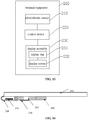
- a terminal equipment 200 is also provided.
- the terminal equipment 200 is used for carrying out the above process of automatically adjusting the display screen brightness of the display device.
- the terminal equipment 200 includes a photoelectric sensor 210, a display assembly 230 and a control device 220.
- Both the photoelectric sensor 210 and the display assembly 230 are electrically connected to the control device 220, and the display assembly 230 includes a display chip 231 and a display screen 232.
- the photoelectric sensor 210 is electrically connected to the control device 220 by a sensor Flexible Circuit Board (FPC) 218, and the display assembly 230 including the display chip 231 and the display screen 232 is electrically connected to the control device 220 by a display FPC.
- FPC Flexible Circuit Board
- the photoelectric sensor 210 senses the ambient light and acquires an optical signal; and the control device 220 compares the optical signal sensed by the photoelectric sensor 210 with a signal stored in the display chip 231, and determines whether or not the irradiation intensity of the ambient light reaches an adjusting threshold. If yes, an adjusting signal is sent to the display chip 231.
- the display chip 231 adjusts a driving current of the display screen 232 according to the adjusting signal, so as to change the brightness of the display screen 232.
- the brightness of the display screen 232 can be adjusted adaptively according to the variance of the ambient light, and this helps to improve the user's comfort experience.
- references terms "an/one embodiment”, “some embodiments”, “an/one example”, or “some examples” refers to that elements, structures, materials, or characteristics described in combination with the embodiment(s) or example(s) are contained in at least one embodiment or at least one example of the present disclosure.
- schematic representations of the above terms are not necessarily aimed at the same embodiment or example.
- the described elements, structures, materials, or characteristics may be combined in an appropriate manner in any one or more embodiments or examples.
- one of ordinary skill in the art can conjoin and combine different embodiments or examples described in this specification, and elements of different embodiments or examples.
Landscapes
- Engineering & Computer Science (AREA)
- Physics & Mathematics (AREA)
- Computer Hardware Design (AREA)
- General Physics & Mathematics (AREA)
- Theoretical Computer Science (AREA)
- Microelectronics & Electronic Packaging (AREA)
- Sustainable Development (AREA)
- Inorganic Chemistry (AREA)
- Chemical & Material Sciences (AREA)
- Life Sciences & Earth Sciences (AREA)
- Devices For Indicating Variable Information By Combining Individual Elements (AREA)
- Electroluminescent Light Sources (AREA)
- Control Of El Displays (AREA)
- Controls And Circuits For Display Device (AREA)
- Control Of Indicators Other Than Cathode Ray Tubes (AREA)
- Liquid Crystal Display Device Control (AREA)
Priority Applications (1)
| Application Number | Priority Date | Filing Date | Title |
|---|---|---|---|
| EP25166069.2A EP4571729A3 (de) | 2018-05-30 | 2019-02-02 | Anzeigevorrichtung, verfahren zur automatischen einstellung der helligkeit eines anzeigebildschirms und endgerät |
Applications Claiming Priority (2)
| Application Number | Priority Date | Filing Date | Title |
|---|---|---|---|
| CN201810539342.9A CN108766387B (zh) | 2018-05-30 | 2018-05-30 | 显示装置、自动调节显示屏亮度的方法及终端设备 |
| PCT/CN2019/074609 WO2019227967A1 (zh) | 2018-05-30 | 2019-02-02 | 显示装置、自动调节显示屏亮度的方法及终端设备 |
Related Child Applications (1)
| Application Number | Title | Priority Date | Filing Date |
|---|---|---|---|
| EP25166069.2A Division EP4571729A3 (de) | 2018-05-30 | 2019-02-02 | Anzeigevorrichtung, verfahren zur automatischen einstellung der helligkeit eines anzeigebildschirms und endgerät |
Publications (2)
| Publication Number | Publication Date |
|---|---|
| EP3806084A1 true EP3806084A1 (de) | 2021-04-14 |
| EP3806084A4 EP3806084A4 (de) | 2022-03-02 |
Family
ID=64004160
Family Applications (2)
| Application Number | Title | Priority Date | Filing Date |
|---|---|---|---|
| EP19750046.5A Pending EP3806084A4 (de) | 2018-05-30 | 2019-02-02 | Anzeigevorrichtung, verfahren zur automatischen anpassung der helligkeit eines bildschirms und endgeräteausrüstung |
| EP25166069.2A Pending EP4571729A3 (de) | 2018-05-30 | 2019-02-02 | Anzeigevorrichtung, verfahren zur automatischen einstellung der helligkeit eines anzeigebildschirms und endgerät |
Family Applications After (1)
| Application Number | Title | Priority Date | Filing Date |
|---|---|---|---|
| EP25166069.2A Pending EP4571729A3 (de) | 2018-05-30 | 2019-02-02 | Anzeigevorrichtung, verfahren zur automatischen einstellung der helligkeit eines anzeigebildschirms und endgerät |
Country Status (5)
| Country | Link |
|---|---|
| US (1) | US11361730B2 (de) |
| EP (2) | EP3806084A4 (de) |
| JP (2) | JP7408394B2 (de) |
| CN (1) | CN108766387B (de) |
| WO (1) | WO2019227967A1 (de) |
Families Citing this family (18)
| Publication number | Priority date | Publication date | Assignee | Title |
|---|---|---|---|---|
| CN108766387B (zh) | 2018-05-30 | 2021-01-22 | 京东方科技集团股份有限公司 | 显示装置、自动调节显示屏亮度的方法及终端设备 |
| CN111243506B (zh) * | 2018-11-29 | 2021-11-02 | 北京小米移动软件有限公司 | 屏幕亮度调整方法、装置、设备及存储介质 |
| CN110008869B (zh) * | 2019-03-25 | 2021-04-30 | 厦门天马微电子有限公司 | 显示面板和显示装置 |
| CN109979414A (zh) * | 2019-03-28 | 2019-07-05 | 深圳市万普拉斯科技有限公司 | 亮度调节方法、装置、移动终端和计算机可读存储介质 |
| CN110197627B (zh) * | 2019-05-30 | 2021-08-13 | 京东方科技集团股份有限公司 | 一种显示基板、显示面板和显示面板的驱动方法 |
| KR20210126840A (ko) * | 2020-04-10 | 2021-10-21 | 삼성디스플레이 주식회사 | 감지 모듈 및 이를 갖는 표시장치 |
| CN111509011A (zh) * | 2020-04-26 | 2020-08-07 | 武汉华星光电半导体显示技术有限公司 | 显示装置及其制备方法 |
| CN111653606B (zh) * | 2020-06-28 | 2022-09-09 | 武汉华星光电技术有限公司 | 集成环境光传感器的显示面板、显示装置及其制备方法 |
| CN112310328B (zh) * | 2020-11-02 | 2023-04-07 | 京东方科技集团股份有限公司 | 一种发光面板及发光装置 |
| CN112420951B (zh) * | 2020-11-18 | 2024-02-13 | 京东方科技集团股份有限公司 | 一种显示装置及其制备方法 |
| EP4113492A1 (de) * | 2021-06-28 | 2023-01-04 | B/E Aerospace, Inc. | Einstellbare anzeige |
| CN113362703B (zh) * | 2021-07-05 | 2022-10-18 | 业成科技(成都)有限公司 | 显示装置及终端设备 |
| CN114205442B (zh) * | 2021-08-23 | 2024-03-15 | 广东夏野日用电器有限公司 | 用于移动终端的视力保护装置及控制方法、装置 |
| CN114882795B (zh) * | 2022-05-24 | 2023-11-24 | 昆山国显光电有限公司 | 显示装置及显示方法 |
| CN117192559B (zh) * | 2022-05-31 | 2026-01-27 | 荣耀终端股份有限公司 | 一种飞行时间测量系统及电子设备 |
| US12488713B2 (en) | 2023-01-12 | 2025-12-02 | Beijing Boe Technology Development Co., Ltd. | Adaptive control device, display apparatus, and adaptive control method |
| CN116068797B (zh) * | 2023-02-24 | 2025-07-18 | 武汉天马微电子有限公司 | 一种显示面板及显示装置 |
| CN119811223A (zh) * | 2023-10-10 | 2025-04-11 | 重庆康佳光电科技有限公司 | 一种显示面板、显示装置及显示面板制造方法 |
Family Cites Families (35)
| Publication number | Priority date | Publication date | Assignee | Title |
|---|---|---|---|---|
| JP2006323199A (ja) | 2005-05-19 | 2006-11-30 | Mitsubishi Electric Corp | 光センサー一体型液晶表示装置 |
| US7619194B2 (en) * | 2007-02-26 | 2009-11-17 | Epson Imaging Devices Corporation | Electro-optical device, semiconductor device, display device, and electronic apparatus having the display device |
| JP5012162B2 (ja) | 2007-04-17 | 2012-08-29 | セイコーエプソン株式会社 | 電気泳動表示装置及び電子機器 |
| JP4661875B2 (ja) | 2008-01-15 | 2011-03-30 | ソニー株式会社 | 表示装置及び表示装置の輝度調整方法 |
| JP2009171167A (ja) | 2008-01-16 | 2009-07-30 | Olympus Imaging Corp | 画像表示装置を有するカメラ |
| JP2009241521A (ja) * | 2008-03-31 | 2009-10-22 | Panasonic Electric Works Co Ltd | 透明基板 |
| KR102113024B1 (ko) * | 2008-09-19 | 2020-06-02 | 가부시키가이샤 한도오따이 에네루기 켄큐쇼 | 표시 장치 |
| JP5509589B2 (ja) | 2008-12-17 | 2014-06-04 | ソニー株式会社 | 表示装置および電子機器 |
| JP2010243647A (ja) | 2009-04-02 | 2010-10-28 | Toppoly Optoelectronics Corp | ディスプレイ装置及びこれを備える電子機器 |
| JP5914069B2 (ja) | 2011-03-17 | 2016-05-11 | 住友化学株式会社 | 金属複合体組成物及びその混合物 |
| JP2014224836A (ja) * | 2011-09-16 | 2014-12-04 | シャープ株式会社 | 発光デバイス、表示装置、照明装置および発電装置 |
| US9024530B2 (en) | 2012-11-13 | 2015-05-05 | Apple Inc. | Synchronized ambient light sensor and display |
| CN104009185A (zh) * | 2013-02-27 | 2014-08-27 | 联想(北京)有限公司 | 一种显示屏及电子设备 |
| JP5604579B2 (ja) * | 2013-10-21 | 2014-10-08 | 株式会社半導体エネルギー研究所 | 表示装置 |
| KR102114727B1 (ko) * | 2013-10-22 | 2020-05-26 | 삼성전자주식회사 | 가속도 센서 운용 방법 및 그 전자 장치 |
| CN105244006B (zh) * | 2014-07-31 | 2018-02-23 | 维沃移动通信有限公司 | 一种显示设备的背光调节方法及其显示设备 |
| JP2016115862A (ja) | 2014-12-17 | 2016-06-23 | セイコーエプソン株式会社 | 画像取得装置、生体情報取得装置、電子機器 |
| CN105870150B (zh) | 2015-02-09 | 2020-09-25 | 三星显示有限公司 | 顶部发光装置和有机发光二极管显示装置 |
| CN104765422A (zh) * | 2015-04-28 | 2015-07-08 | 小米科技有限责任公司 | 移动设备的屏幕模组和移动设备 |
| CN106200086B (zh) * | 2015-04-30 | 2019-12-13 | 小米科技有限责任公司 | 液晶显示组件及电子设备 |
| CN105094465B (zh) * | 2015-08-12 | 2018-02-02 | 小米科技有限责任公司 | 环境光测量方法及装置 |
| JP6727622B2 (ja) | 2015-09-28 | 2020-07-22 | 華為技術有限公司Huawei Technologies Co.,Ltd. | 端末および周囲光の輝度を検出するための方法 |
| JP2017174553A (ja) * | 2016-03-22 | 2017-09-28 | 株式会社ジャパンディスプレイ | 表示装置 |
| CN107783221A (zh) * | 2016-08-29 | 2018-03-09 | 京东方科技集团股份有限公司 | 显示模组 |
| KR102694995B1 (ko) * | 2016-08-30 | 2024-08-14 | 삼성전자주식회사 | 디스플레이와 센서를 포함하는 전자 장치 및 그 동작 방법 |
| CN106444998B (zh) * | 2016-12-06 | 2023-10-13 | Oppo广东移动通信有限公司 | 一种面板、传感器组件及移动终端 |
| CN106713654A (zh) | 2017-01-11 | 2017-05-24 | 维沃移动通信有限公司 | 一种移动终端显示调整的方法及移动终端 |
| CN107133613B (zh) * | 2017-06-06 | 2020-06-30 | 上海天马微电子有限公司 | 一种显示面板及显示装置 |
| US10553179B2 (en) * | 2017-09-08 | 2020-02-04 | Apple Inc. | Electronic devices with ambient light sensors |
| CN107909922B (zh) * | 2017-11-16 | 2019-10-15 | 维沃移动通信有限公司 | 一种移动终端 |
| CN107767835B (zh) * | 2017-11-22 | 2020-04-10 | Oppo广东移动通信有限公司 | 显示屏组件及电子设备 |
| CN107979698B (zh) * | 2017-11-22 | 2020-05-12 | Oppo广东移动通信有限公司 | 环境光强度检测方法、装置、存储介质及电子设备 |
| CN107911506A (zh) * | 2017-11-22 | 2018-04-13 | 维沃移动通信有限公司 | 移动终端及其屏幕显示亮度的调节方法 |
| CN108051370A (zh) * | 2017-11-30 | 2018-05-18 | 北京小米移动软件有限公司 | 环境光检测方法及装置、电子设备 |
| CN108766387B (zh) * | 2018-05-30 | 2021-01-22 | 京东方科技集团股份有限公司 | 显示装置、自动调节显示屏亮度的方法及终端设备 |
-
2018
- 2018-05-30 CN CN201810539342.9A patent/CN108766387B/zh active Active
-
2019
- 2019-02-02 EP EP19750046.5A patent/EP3806084A4/de active Pending
- 2019-02-02 EP EP25166069.2A patent/EP4571729A3/de active Pending
- 2019-02-02 US US16/490,620 patent/US11361730B2/en active Active
- 2019-02-02 WO PCT/CN2019/074609 patent/WO2019227967A1/zh not_active Ceased
- 2019-02-02 JP JP2019547309A patent/JP7408394B2/ja active Active
-
2023
- 2023-12-18 JP JP2023212635A patent/JP7721623B2/ja active Active
Also Published As
| Publication number | Publication date |
|---|---|
| US20210358453A1 (en) | 2021-11-18 |
| JP7721623B2 (ja) | 2025-08-12 |
| CN108766387A (zh) | 2018-11-06 |
| JP2024041763A (ja) | 2024-03-27 |
| EP4571729A3 (de) | 2025-09-24 |
| JP7408394B2 (ja) | 2024-01-05 |
| CN108766387B (zh) | 2021-01-22 |
| WO2019227967A1 (zh) | 2019-12-05 |
| EP4571729A2 (de) | 2025-06-18 |
| EP3806084A4 (de) | 2022-03-02 |
| US11361730B2 (en) | 2022-06-14 |
| JP2021524922A (ja) | 2021-09-16 |
Similar Documents
| Publication | Publication Date | Title |
|---|---|---|
| US11361730B2 (en) | Display device, method of automatically adjusting brightness of display screen, and terminal equipment | |
| US20210142028A1 (en) | Optical fingerprint identification apparatus and electronic device | |
| AU2018372452B2 (en) | Display screen component and electronic device | |
| EP3822738B1 (de) | Bildschirmanordnung, elektronische vorrichtung und steuerverfahren für eine elektronische vorrichtung | |
| CN108983468A (zh) | 一种显示装置 | |
| US12279505B2 (en) | Display device and touch controller | |
| US11569290B2 (en) | Sensing device and display apparatus including the same | |
| CN107978261B (zh) | 电子设备 | |
| CN108566460B (zh) | 显示屏组件及电子设备 | |
| CN112864214B (zh) | 显示模组及显示装置 | |
| KR20260042367A (ko) | 표시 패널 및 이를 포함하는 전자 장치 | |
| CN111626214A (zh) | 屏下指纹识别装置及系统、指纹识别方法和电子装置 | |
| WO2021136342A1 (zh) | 指纹识别器件、指纹识别显示基板及其制作方法 | |
| KR102542872B1 (ko) | 지문 센싱 모듈 및 광학식 이미지 센서 내장형 표시장치 | |
| CN111294435B (zh) | 移动终端 | |
| US11200397B2 (en) | Fingerprint identification assembly, display substrate, display panel and fingerprint identification method | |
| CN212412088U (zh) | 显示面板、显示屏和终端 | |
| CN111381725B (zh) | 具有光学扫描功能的触控板 | |
| WO2021237521A1 (zh) | 屏下指纹识别装置及系统、指纹识别方法和电子装置 | |
| CN107945662B (zh) | 显示屏、显示屏组件及电子设备 | |
| CN107608122B (zh) | 显示屏、功能组件及移动终端 | |
| CN111308782B (zh) | 电子设备 | |
| US20250204230A1 (en) | Light emitting display device | |
| CN114122103B (zh) | 显示面板及其制备方法、显示装置 | |
| EP4546990A1 (de) | Lichtemittierende anzeigevorrichtung |
Legal Events
| Date | Code | Title | Description |
|---|---|---|---|
| STAA | Information on the status of an ep patent application or granted ep patent |
Free format text: STATUS: UNKNOWN |
|
| STAA | Information on the status of an ep patent application or granted ep patent |
Free format text: STATUS: THE INTERNATIONAL PUBLICATION HAS BEEN MADE |
|
| PUAI | Public reference made under article 153(3) epc to a published international application that has entered the european phase |
Free format text: ORIGINAL CODE: 0009012 |
|
| STAA | Information on the status of an ep patent application or granted ep patent |
Free format text: STATUS: REQUEST FOR EXAMINATION WAS MADE |
|
| 17P | Request for examination filed |
Effective date: 20190816 |
|
| AK | Designated contracting states |
Kind code of ref document: A1 Designated state(s): AL AT BE BG CH CY CZ DE DK EE ES FI FR GB GR HR HU IE IS IT LI LT LU LV MC MK MT NL NO PL PT RO RS SE SI SK SM TR |
|
| AX | Request for extension of the european patent |
Extension state: BA ME |
|
| DAV | Request for validation of the european patent (deleted) | ||
| DAX | Request for extension of the european patent (deleted) | ||
| RIN1 | Information on inventor provided before grant (corrected) |
Inventor name: LIU, FEI Inventor name: HSIEH, MING CHE Inventor name: SUN, KUO Inventor name: SUN, YANLIU |
|
| A4 | Supplementary search report drawn up and despatched |
Effective date: 20220202 |
|
| RIC1 | Information provided on ipc code assigned before grant |
Ipc: G09G 3/3208 20160101ALI20220127BHEP Ipc: G09G 3/20 20060101ALI20220127BHEP Ipc: H01L 27/32 20060101ALI20220127BHEP Ipc: G09G 5/10 20060101AFI20220127BHEP |
|
| STAA | Information on the status of an ep patent application or granted ep patent |
Free format text: STATUS: EXAMINATION IS IN PROGRESS |
|
| 17Q | First examination report despatched |
Effective date: 20250103 |