EP3807718B1 - Réflecteur et procédé de fabrication d'un réflecteur - Google Patents
Réflecteur et procédé de fabrication d'un réflecteur Download PDFInfo
- Publication number
- EP3807718B1 EP3807718B1 EP19725992.2A EP19725992A EP3807718B1 EP 3807718 B1 EP3807718 B1 EP 3807718B1 EP 19725992 A EP19725992 A EP 19725992A EP 3807718 B1 EP3807718 B1 EP 3807718B1
- Authority
- EP
- European Patent Office
- Prior art keywords
- surface part
- reflector
- mandrel
- optical surface
- optical
- Prior art date
- Legal status (The legal status is an assumption and is not a legal conclusion. Google has not performed a legal analysis and makes no representation as to the accuracy of the status listed.)
- Active
Links
Images



Classifications
-
- G—PHYSICS
- G21—NUCLEAR PHYSICS; NUCLEAR ENGINEERING
- G21K—HANDLING OF PARTICLES OR IONISING RADIATION NOT OTHERWISE PROVIDED FOR; IRRADIATION DEVICES; GAMMA RAY OR X-RAY MICROSCOPES
- G21K1/00—Arrangements for handling particles or ionising radiation, e.g. focusing or moderating
- G21K1/06—Arrangements for handling particles or ionising radiation, e.g. focusing or moderating using diffraction, refraction or reflection, e.g. monochromators
-
- B—PERFORMING OPERATIONS; TRANSPORTING
- B24—GRINDING; POLISHING
- B24C—ABRASIVE OR RELATED BLASTING WITH PARTICULATE MATERIAL
- B24C1/00—Methods for use of abrasive blasting for producing particular effects; Use of auxiliary equipment in connection with such methods
- B24C1/08—Methods for use of abrasive blasting for producing particular effects; Use of auxiliary equipment in connection with such methods for polishing surfaces, e.g. smoothing a surface by making use of liquid-borne abrasives
-
- G—PHYSICS
- G01—MEASURING; TESTING
- G01N—INVESTIGATING OR ANALYSING MATERIALS BY DETERMINING THEIR CHEMICAL OR PHYSICAL PROPERTIES
- G01N21/00—Investigating or analysing materials by the use of optical means, i.e. using sub-millimetre waves, infrared, visible or ultraviolet light
- G01N21/84—Systems specially adapted for particular applications
- G01N21/88—Investigating the presence of flaws or contamination
- G01N21/95—Investigating the presence of flaws or contamination characterised by the material or shape of the object to be examined
- G01N21/9501—Semiconductor wafers
-
- G—PHYSICS
- G01—MEASURING; TESTING
- G01N—INVESTIGATING OR ANALYSING MATERIALS BY DETERMINING THEIR CHEMICAL OR PHYSICAL PROPERTIES
- G01N21/00—Investigating or analysing materials by the use of optical means, i.e. using sub-millimetre waves, infrared, visible or ultraviolet light
- G01N21/84—Systems specially adapted for particular applications
- G01N21/88—Investigating the presence of flaws or contamination
- G01N21/95—Investigating the presence of flaws or contamination characterised by the material or shape of the object to be examined
- G01N21/956—Inspecting patterns on the surface of objects
-
- G—PHYSICS
- G03—PHOTOGRAPHY; CINEMATOGRAPHY; ANALOGOUS TECHNIQUES USING WAVES OTHER THAN OPTICAL WAVES; ELECTROGRAPHY; HOLOGRAPHY
- G03F—PHOTOMECHANICAL PRODUCTION OF TEXTURED OR PATTERNED SURFACES, e.g. FOR PRINTING, FOR PROCESSING OF SEMICONDUCTOR DEVICES; MATERIALS THEREFOR; ORIGINALS THEREFOR; APPARATUS SPECIALLY ADAPTED THEREFOR
- G03F7/00—Photomechanical, e.g. photolithographic, production of textured or patterned surfaces, e.g. printing surfaces; Materials therefor, e.g. comprising photoresists; Apparatus specially adapted therefor
- G03F7/70—Microphotolithographic exposure; Apparatus therefor
- G03F7/70058—Mask illumination systems
- G03F7/7015—Details of optical elements
- G03F7/70166—Capillary or channel elements, e.g. nested extreme ultraviolet [EUV] mirrors or shells, optical fibers or light guides
-
- G—PHYSICS
- G03—PHOTOGRAPHY; CINEMATOGRAPHY; ANALOGOUS TECHNIQUES USING WAVES OTHER THAN OPTICAL WAVES; ELECTROGRAPHY; HOLOGRAPHY
- G03F—PHOTOMECHANICAL PRODUCTION OF TEXTURED OR PATTERNED SURFACES, e.g. FOR PRINTING, FOR PROCESSING OF SEMICONDUCTOR DEVICES; MATERIALS THEREFOR; ORIGINALS THEREFOR; APPARATUS SPECIALLY ADAPTED THEREFOR
- G03F7/00—Photomechanical, e.g. photolithographic, production of textured or patterned surfaces, e.g. printing surfaces; Materials therefor, e.g. comprising photoresists; Apparatus specially adapted therefor
- G03F7/70—Microphotolithographic exposure; Apparatus therefor
- G03F7/70483—Information management; Active and passive control; Testing; Wafer monitoring, e.g. pattern monitoring
- G03F7/70605—Workpiece metrology
- G03F7/70616—Monitoring the printed patterns
- G03F7/70625—Dimensions, e.g. line width, critical dimension [CD], profile, sidewall angle or edge roughness
-
- G—PHYSICS
- G03—PHOTOGRAPHY; CINEMATOGRAPHY; ANALOGOUS TECHNIQUES USING WAVES OTHER THAN OPTICAL WAVES; ELECTROGRAPHY; HOLOGRAPHY
- G03F—PHOTOMECHANICAL PRODUCTION OF TEXTURED OR PATTERNED SURFACES, e.g. FOR PRINTING, FOR PROCESSING OF SEMICONDUCTOR DEVICES; MATERIALS THEREFOR; ORIGINALS THEREFOR; APPARATUS SPECIALLY ADAPTED THEREFOR
- G03F7/00—Photomechanical, e.g. photolithographic, production of textured or patterned surfaces, e.g. printing surfaces; Materials therefor, e.g. comprising photoresists; Apparatus specially adapted therefor
- G03F7/70—Microphotolithographic exposure; Apparatus therefor
- G03F7/70483—Information management; Active and passive control; Testing; Wafer monitoring, e.g. pattern monitoring
- G03F7/70605—Workpiece metrology
- G03F7/706843—Metrology apparatus
- G03F7/706847—Production of measurement radiation, e.g. synchrotron, free-electron laser, plasma source or higher harmonic generation [HHG]
-
- G—PHYSICS
- G03—PHOTOGRAPHY; CINEMATOGRAPHY; ANALOGOUS TECHNIQUES USING WAVES OTHER THAN OPTICAL WAVES; ELECTROGRAPHY; HOLOGRAPHY
- G03F—PHOTOMECHANICAL PRODUCTION OF TEXTURED OR PATTERNED SURFACES, e.g. FOR PRINTING, FOR PROCESSING OF SEMICONDUCTOR DEVICES; MATERIALS THEREFOR; ORIGINALS THEREFOR; APPARATUS SPECIALLY ADAPTED THEREFOR
- G03F7/00—Photomechanical, e.g. photolithographic, production of textured or patterned surfaces, e.g. printing surfaces; Materials therefor, e.g. comprising photoresists; Apparatus specially adapted therefor
- G03F7/70—Microphotolithographic exposure; Apparatus therefor
- G03F7/70483—Information management; Active and passive control; Testing; Wafer monitoring, e.g. pattern monitoring
- G03F7/70605—Workpiece metrology
- G03F7/706843—Metrology apparatus
- G03F7/706849—Irradiation branch, e.g. optical system details, illumination mode or polarisation control
-
- G—PHYSICS
- G03—PHOTOGRAPHY; CINEMATOGRAPHY; ANALOGOUS TECHNIQUES USING WAVES OTHER THAN OPTICAL WAVES; ELECTROGRAPHY; HOLOGRAPHY
- G03F—PHOTOMECHANICAL PRODUCTION OF TEXTURED OR PATTERNED SURFACES, e.g. FOR PRINTING, FOR PROCESSING OF SEMICONDUCTOR DEVICES; MATERIALS THEREFOR; ORIGINALS THEREFOR; APPARATUS SPECIALLY ADAPTED THEREFOR
- G03F7/00—Photomechanical, e.g. photolithographic, production of textured or patterned surfaces, e.g. printing surfaces; Materials therefor, e.g. comprising photoresists; Apparatus specially adapted therefor
- G03F7/70—Microphotolithographic exposure; Apparatus therefor
- G03F7/708—Construction of apparatus, e.g. environment aspects, hygiene aspects or materials
- G03F7/7095—Materials, e.g. materials for housing, stage or other support having particular properties, e.g. weight, strength, conductivity, thermal expansion coefficient
- G03F7/70958—Optical materials or coatings, e.g. with particular transmittance, reflectance or anti-reflection properties
-
- G—PHYSICS
- G21—NUCLEAR PHYSICS; NUCLEAR ENGINEERING
- G21K—HANDLING OF PARTICLES OR IONISING RADIATION NOT OTHERWISE PROVIDED FOR; IRRADIATION DEVICES; GAMMA RAY OR X-RAY MICROSCOPES
- G21K1/00—Arrangements for handling particles or ionising radiation, e.g. focusing or moderating
- G21K1/06—Arrangements for handling particles or ionising radiation, e.g. focusing or moderating using diffraction, refraction or reflection, e.g. monochromators
- G21K1/062—Devices having a multilayer structure
-
- G—PHYSICS
- G21—NUCLEAR PHYSICS; NUCLEAR ENGINEERING
- G21K—HANDLING OF PARTICLES OR IONISING RADIATION NOT OTHERWISE PROVIDED FOR; IRRADIATION DEVICES; GAMMA RAY OR X-RAY MICROSCOPES
- G21K1/00—Arrangements for handling particles or ionising radiation, e.g. focusing or moderating
- G21K1/06—Arrangements for handling particles or ionising radiation, e.g. focusing or moderating using diffraction, refraction or reflection, e.g. monochromators
- G21K1/067—Arrangements for handling particles or ionising radiation, e.g. focusing or moderating using diffraction, refraction or reflection, e.g. monochromators using surface reflection, e.g. grazing incidence mirrors, gratings
-
- G—PHYSICS
- G21—NUCLEAR PHYSICS; NUCLEAR ENGINEERING
- G21K—HANDLING OF PARTICLES OR IONISING RADIATION NOT OTHERWISE PROVIDED FOR; IRRADIATION DEVICES; GAMMA RAY OR X-RAY MICROSCOPES
- G21K2201/00—Arrangements for handling radiation or particles
- G21K2201/06—Arrangements for handling radiation or particles using diffractive, refractive or reflecting elements
- G21K2201/064—Arrangements for handling radiation or particles using diffractive, refractive or reflecting elements having a curved surface
-
- G—PHYSICS
- G21—NUCLEAR PHYSICS; NUCLEAR ENGINEERING
- G21K—HANDLING OF PARTICLES OR IONISING RADIATION NOT OTHERWISE PROVIDED FOR; IRRADIATION DEVICES; GAMMA RAY OR X-RAY MICROSCOPES
- G21K2201/00—Arrangements for handling radiation or particles
- G21K2201/06—Arrangements for handling radiation or particles using diffractive, refractive or reflecting elements
- G21K2201/067—Construction details
Definitions
- the present invention relates to reflectors and methods of manufacturing reflectors, especially oblique incidence and grazing incidence reflectors for hard X-rays, soft x-rays, EUV radiation and/or neutrons.
- US 2009/272917 A1 discloses a reflector comprising a hollow body having an interior surface defining a passage through the hollow body, the interior surface having at least one optical surface part configured to reflect radiation and a supporter surface part, wherein the optical surface part has a predetermined optical power and the supporter surface part does not have the predetermined optical power.
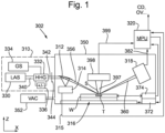
- the filtered beam 342 enters an inspection chamber 350 where the substrate W including a structure of interest is held for inspection at a measurement position by substrate support 316.
- the structure of interest is labeled T.
- the gas pressure within inspection chamber 350 is maintained near vacuum by vacuum pump 352, so that EUV radiation can pass through the focusing system without undue attenuation.
- the illumination system 312 has the function of focusing the radiation into a focused beam 356, and may comprise for example a twodimensionally curved mirror, or a series of one-dimensionally curved mirrors, as described in published US patent application US2017/0184981A1 .
- Reflected radiation 360 is captured by detector 318 and a spectrum 382 is provided to processing unit 320 for use in calculating a property of the target structure T.
- the illumination system 312 and detection system 318 thus form an inspection apparatus.
- This inspection apparatus may comprise a soft X-ray and/or EUV spectroscopic reflectometer of the kind described in US2016 282282A1 .
- FIG. 1 a single further detection system 398 is drawn, but embodiments of the inspection apparatus 302 may comprise a plurality of further detection systems 398 that are arranged at different position to detect and/or image diffracted radiation 397 at a plurality of diffraction directions.
- the (higher) diffraction orders of the focussed radiation beam that impinges on the target T are detected and/or imaged by one or more further detection systems 398.
- the one or more detection systems 398 generate a signal 399 that is provided to the metrology processing unit 320.
- the signal 399 may include information of the diffracted light 397 and/or may include images obtained from the diffracted light 397.
- the inspection apparatus uses soft X-ray and/or EUV radiation at any suitable incidence, e.g. normal incidence, near-normal incidence or grazing incidence, for example to perform diffraction-based measurements of asymmetry.
- the angle of incidence may also be in the range from 20 to 40 degrees, for example, 30 degrees.
- the inspection apparatus can be provided in a hybrid metrology system.
- Performance parameters to be measured can include overlay (OVL), critical dimension (CD) Via Contact Landing (a combination of CD and OVL) and CD uniformity (CDU).
- Measurement techniques can include coherent diffraction imaging (CDI) and at-resolution overlay (ARO) metrology.
- the illuminator is able to focus more than 99% of the radiation in a metrology target on the wafer with dimensions between approximately 2x2 ⁇ m 2 and 40x40 ⁇ m 2 .
- the relevant surface roughness of the reflectors be better than 100 pm RMS, optionally better than 50 pm RMS and most optionally better than 35 pm RMS.
- the relevant RMS surface roughness is obtained by integration of the power spectral density (PSD) of a measured surface profile.
- a conventional approach to manufacturing reflectors for an EUV or soft x-ray inspection apparatus involves polishing a blank to the desired figure and degree of flatness. This can take a very long time and is expensive.
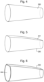
- an inverse optical surface is formed on the preform 200, as shown in Figure 5 , by removing material from one side.
- the inverse optical surface can be formed with a two step process wherein conventional grinding techniques are used to achieve a figure close to the desired end figure and then a super polishing technique is used to achieve the finally desired figure (within desired figure error limits) and degree of roughness.
- the inverse optical surface optionally has a roughness less than 100 pm RMS, optionally less than 50 pm RMS, optionally less than 35 pm RMS.
- the shape of the inverse optical surface is the inverse of the surface of the reflector that is to be manufactured.
- Suitable super polishing techniques that can be used in the invention include: Magneto-Rheological Fluid Finishing (MRF), Fluid Jet Polishing (FJP), Elastic Emission Machining (EEM), Ion Beam Figuring and Float Polishing.
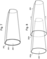
- the shell can be formed of a resin which is applied to the mandrel and cured using known techniques.
- Another possibility is to form the shell from glass or a thermoplastic polymer.
- a heated glass tube of diameter slightly larger than the mandrel is placed around the mandrel.
- the space between the glass tube and the mandrel is evacuated so that external pressure forces the heated glass tube to conform to the shape of the mandrel and in particular the inverse optical surface.
- the glass shell is then cooled so as to take a permanent shape defined by the mandrel.
- a similar process can be followed in which the initial tube is made from a thermoplastic polymer instead of glass.
- the optical surface part 204 can be provided with a reflection enhancing coating, e.g. or gold or ruthenium, if desired.
- a reflection enhancing coating e.g. or gold or ruthenium
- Such a coating can be applied selectively to the optical surface part 204 or to the whole of the interior surface of the shell and even to the outer surface, e.g. if that is easier than a selective coating.
- the coating thickness need not be large so the material cost is not high even if the whole shell is coated.
- the reflector has a reflectivity at grazing incidence to at least one wavelength in the soft x-ray or EUV range of greater than about 70%, optionally greater than about 80%.
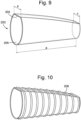
- Figure 13 shows two full-shell reflectors 203a, 203b configured as a Kirkpatrick-Baez crossed mirror pair for use in the illumination system of an inspection apparatus, such as metrology apparatus.
- the curvature of the optical surface parts 204 is not shown to scale.
- the full-shell reflectors 203a, 203b may be oriented differently, e.g. with both narrow ends adjacent. Since the reflectors are grazing-incidence reflectors, beam angles are low and the non-optical surface parts 205 will not usually interfere with the beam path. However, if necessary parts of the non-optical surface can be cut away to avoid occluding the beam or to avoid interference with other components of the apparatus.
- a useful grating may have a depth of no more than 10 nm so that replication and release (using thermal expansion) should be possible without too much trouble.
- projection system PS used herein should be broadly interpreted as encompassing various types of projection system, including refractive, reflective, catadioptric, anamorphic, magnetic, electromagnetic and/or electrostatic optical systems, or any combination thereof, as appropriate for the exposure radiation being used, and/or for other factors such as the use of an immersion liquid or the use of a vacuum. Any use of the term “projection lens” herein may be considered as synonymous with the more general term “projection system” PS.
- Targets may have smaller sub-segmentation which are configured to mimic dimensions of the functional part of the design layout in a target. Due to this sub-segmentation, the targets will behave more similar to the functional part of the design layout such that the overall process parameter measurements resembles the functional part of the design layout better.
- the targets may be measured in an underfilled mode or in an overfilled mode. In the underfilled mode, the measurement beam generates a spot that is smaller than the overall target. In the overfilled mode, the measurement beam generates a spot that is larger than the overall target. In such overfilled mode, it may also be possible to measure different targets simultaneously, thus determining different processing parameters at the same time.
- HHG refers to High Harmonic Generation, which is also sometimes referred to as high order harmonic generation.
- HHG is a non-linear process in which a target, for example a gas, a plasma or a solid sample, is illuminated by an intensive laser pulse. Subsequently, the target may emit radiation with a frequency that is a multiple of the frequency of the radiation of the laser pulse. Such frequency, that is a multiple, is called a harmonic of the radiation of the laser pulse. Harmonics above the fifth harmonic may be referred to as high harmonics and radiation containing them as HHG radiation.
- Neon is used as a gas target, all radiation with a wavelength shorter than 62 nm (having a photon energy higher than 20.18 eV) is generated by means of the HHG process.
- Argon all radiation having a photon energy higher than about 15.8 eV is generated by means of the HHG process.
Landscapes
- Physics & Mathematics (AREA)
- General Physics & Mathematics (AREA)
- Engineering & Computer Science (AREA)
- High Energy & Nuclear Physics (AREA)
- Spectroscopy & Molecular Physics (AREA)
- General Engineering & Computer Science (AREA)
- Health & Medical Sciences (AREA)
- Analytical Chemistry (AREA)
- General Health & Medical Sciences (AREA)
- Pathology (AREA)
- Immunology (AREA)
- Biochemistry (AREA)
- Chemical & Material Sciences (AREA)
- Life Sciences & Earth Sciences (AREA)
- Mechanical Engineering (AREA)
- Public Health (AREA)
- Epidemiology (AREA)
- Environmental & Geological Engineering (AREA)
- Optics & Photonics (AREA)
- Plasma & Fusion (AREA)
- Exposure And Positioning Against Photoresist Photosensitive Materials (AREA)
- Optical Elements Other Than Lenses (AREA)
- Investigating Or Analysing Materials By Optical Means (AREA)
Claims (15)
- Un réflecteur comprenant un corps creux (203) ayant une surface intérieure qui définit un passage au travers du corps creux, la surface intérieure ayant au moins une partie de surface optique (204) configurée pour réfléchir un rayonnement et une partie de surface supportrice (205), où la partie de surface optique a une puissance optique prédéterminée et la partie de surface supportrice n'a pas la puissance optique prédéterminée, la partie de surface supportrice ayant pour fonction de supporter la partie de surface optique.
- Un réflecteur selon la revendication 1 où la ou les parties de surface optique ont une première rugosité et la partie de surface supportrice a une deuxième rugosité, la première rugosité étant plus faible que la deuxième rugosité ;
et, facultativement, la première rugosité est inférieure à 100 pm RMS (Root Mean Square, valeur quadratique moyenne), facultativement, inférieure à 50 pm RMS, facultativement inférieure à 35 pm RMS. - Un réflecteur selon la revendication 1 ou la revendication 2 où la partie de surface optique a un premier rayon de courbure dans un plan perpendiculaire à un axe du passage, et la partie de surface supportrice a un deuxième rayon de courbure dans le plan, la valeur absolue du premier rayon de courbure étant supérieure au deuxième rayon de courbure.
- Un réflecteur selon la revendication 3 où la section transversale de la partie de surface supportrice dans le plan sous-tend un angle supérieur à 180° au niveau de l'axe.
- Un réflecteur selon n'importe laquelle des revendications précédentes où la section transversale du passage croît de façon monotone d'une extrémité de celui-ci à l'autre.
- Un réflecteur selon n'importe laquelle des revendications précédentes comprenant en sus une couche amplifiant la réflexion fournie sur la partie de surface optique.
- Un réflecteur selon n'importe laquelle des revendications précédentes où le corps comprend une coque formée en un matériau sélectionné dans le groupe constitué : de nickel, de résine, de verre et de polymères thermoplastiques ;
et, facultativement, le réflecteur comprenant en sus un renfort à l'extérieur de la coque. - Un réflecteur selon n'importe laquelle des revendications précédentes où la partie de surface optique a une réflectivité à une incidence rasante supérieure à 70 % à une longueur d'onde comprise dans l'intervalle allant de 1 nm à 50 nm, facultativement supérieure à 80 %.
- Une unité optique comprenant deux réflecteurs (203a, 203b) selon n'importe laquelle des revendications précédentes, où les deux réflecteurs sont agencés de telle sorte qu'un réflecteur réfléchit de la lumière vers l'autre et que les plans méridiens des deux réflecteurs sont perpendiculaires.
- Un appareil d'inspection comprenant un système optique incluant un réflecteur selon n'importe laquelle des revendications 1 à 8 ou une unité optique selon la revendication 9.
- Un procédé de fabrication d'un réflecteur, le procédé comprenant :la fourniture d'un mandrin (200) axialement symétrique ;la mise en forme d'une partie de la surface circonférentielle du mandrin afin de former au moins une partie de surface optique inverse qui n'est pas rotationnellement symétrique autour de l'axe du mandrin ;la formation d'un corps de réflecteur (203) autour du mandrin ; etla séparation du corps de réflecteur du mandrin en vertu de quoi le corps de réflecteur a une surface optique définie par la partie de surface optique inverse et une partie de surface supportrice définie par le reste de la surface externe du mandrin.
- Un procédé selon la revendication 11 où la mise en forme d'une partie de la surface externe du mandrin comprend une étape de super polissage utilisant un processus sélectionné dans le groupe constitué : de la finition par fluide magnéto-rhéologique (MRF, Magneto-Rheological Fluid Finishing), du polissage par jet de fluide (FJP, Fluid Jet Polishing), de l'usinage par émission élastique (EEM, Elastic Emission Machining), du façonnage par faisceau d'ions (Ion Beam Figuring) et du polissage par flottation (Float Polishing).
- Un procédé selon la revendication 11 où l'étape de super polissage est réalisée de sorte que la partie de surface optique inverse a une rugosité de surface inférieure à 100 pm RMS, facultativement, inférieure à 50 pm RMS, facultativement inférieure à 35 pm RMS.
- Un procédé selon n'importe laquelle de la revendication 11, de la revendication 12 ou de la revendication 13 comprenant en sus l'application d'un revêtement mono- ou multicouche amplifiant la réflexion sur la partie de surface optique du corps de réflecteur.
- Un procédé selon n'importe laquelle des revendications 11 à 14 comprenant en sus l'application d'une couche faisant office d'électrode et de couche de séparation (202) sur le mandrin après la mise en forme et avant la formation.
Applications Claiming Priority (2)
| Application Number | Priority Date | Filing Date | Title |
|---|---|---|---|
| EP18178127.9A EP3582009A1 (fr) | 2018-06-15 | 2018-06-15 | Réflecteur et procédé de fabrication d'un réflecteur |
| PCT/EP2019/063352 WO2019238382A1 (fr) | 2018-06-15 | 2019-05-23 | Réflecteur et procédé de fabrication de réflecteur |
Publications (2)
| Publication Number | Publication Date |
|---|---|
| EP3807718A1 EP3807718A1 (fr) | 2021-04-21 |
| EP3807718B1 true EP3807718B1 (fr) | 2025-04-09 |
Family
ID=62705440
Family Applications (2)
| Application Number | Title | Priority Date | Filing Date |
|---|---|---|---|
| EP18178127.9A Withdrawn EP3582009A1 (fr) | 2018-06-15 | 2018-06-15 | Réflecteur et procédé de fabrication d'un réflecteur |
| EP19725992.2A Active EP3807718B1 (fr) | 2018-06-15 | 2019-05-23 | Réflecteur et procédé de fabrication d'un réflecteur |
Family Applications Before (1)
| Application Number | Title | Priority Date | Filing Date |
|---|---|---|---|
| EP18178127.9A Withdrawn EP3582009A1 (fr) | 2018-06-15 | 2018-06-15 | Réflecteur et procédé de fabrication d'un réflecteur |
Country Status (8)
| Country | Link |
|---|---|
| US (2) | US11145428B2 (fr) |
| EP (2) | EP3582009A1 (fr) |
| JP (1) | JP7286683B2 (fr) |
| KR (1) | KR102579721B1 (fr) |
| CN (1) | CN112292639B (fr) |
| IL (1) | IL279369B2 (fr) |
| TW (1) | TWI742384B (fr) |
| WO (1) | WO2019238382A1 (fr) |
Families Citing this family (5)
| Publication number | Priority date | Publication date | Assignee | Title |
|---|---|---|---|---|
| EP3582009A1 (fr) * | 2018-06-15 | 2019-12-18 | ASML Netherlands B.V. | Réflecteur et procédé de fabrication d'un réflecteur |
| US11680909B2 (en) * | 2020-05-14 | 2023-06-20 | The Boeing Company | Automated inspection of foreign materials, cracks and other surface anomalies |
| JP2023530924A (ja) * | 2020-06-11 | 2023-07-20 | アンドリュー ヒン チョン クン | 光源発生装置、光源発生方法及び関連する検出システム |
| WO2024170230A1 (fr) | 2023-02-13 | 2024-08-22 | Asml Netherlands B.V. | Procédé de métrologie et outil de métrologie associé |
| EP4414785A1 (fr) | 2023-02-13 | 2024-08-14 | ASML Netherlands B.V. | Procédé de métrologie avec faisceaux incident à une cible sous une pluralité de différents angles d'incidence et outil de métrologie associé |
Family Cites Families (50)
| Publication number | Priority date | Publication date | Assignee | Title |
|---|---|---|---|---|
| US3872349A (en) * | 1973-03-29 | 1975-03-18 | Fusion Systems Corp | Apparatus and method for generating radiation |
| US5001737A (en) * | 1988-10-24 | 1991-03-19 | Aaron Lewis | Focusing and guiding X-rays with tapered capillaries |
| EP0723272B1 (fr) * | 1994-07-08 | 2001-04-25 | Muradin Abubekirovich Kumakhov | Procede de guidage de faisceaux de particules neutres et chargees et son dispositif de mise en uvre |
| US5741445A (en) * | 1996-02-06 | 1998-04-21 | Cvd, Incorporated | Method of making lightweight closed-back mirror |
| US6859328B2 (en) * | 1998-05-05 | 2005-02-22 | Carl Zeiss Semiconductor | Illumination system particularly for microlithography |
| US6118130A (en) * | 1998-11-18 | 2000-09-12 | Fusion Uv Systems, Inc. | Extendable focal length lamp |
| US6278764B1 (en) * | 1999-07-22 | 2001-08-21 | The Regents Of The Unviersity Of California | High efficiency replicated x-ray optics and fabrication method |
| EP1152555A1 (fr) * | 2000-05-03 | 2001-11-07 | Media Lario S.r.L. | Miroir de telescope pour la transmission de données optiques de grande largeur de bande dans l'espace libre |
| US6847700B1 (en) * | 2001-01-19 | 2005-01-25 | Florida Institute Of Technology | Method and apparatus for delivery of x-ray irradiation |
| SG135052A1 (en) | 2002-11-12 | 2007-09-28 | Asml Netherlands Bv | Lithographic apparatus and device manufacturing method |
| FR2866438B1 (fr) * | 2004-02-16 | 2006-08-11 | Agence Spatiale Europeenne | Element optique reflecteur, son procede de fabrication, et instrument optique mettant en oeuvre de tels elements |
| JP2007536552A (ja) | 2004-05-10 | 2007-12-13 | コーニンクレッカ フィリップス エレクトロニクス エヌ ヴィ | 光学精密測定装置及び方法 |
| US7791727B2 (en) | 2004-08-16 | 2010-09-07 | Asml Netherlands B.V. | Method and apparatus for angular-resolved spectroscopic lithography characterization |
| US8142691B2 (en) * | 2004-09-30 | 2012-03-27 | Lawrence Livermore National Security, Llc | Thermal casting of polymers in centrifuge for producing X-ray optics |
| US20080099935A1 (en) * | 2004-11-09 | 2008-05-01 | Wilhelm Egle | High-Precision Optical Surface Prepared by Sagging from a Masterpiece |
| US20090225400A1 (en) | 2004-12-09 | 2009-09-10 | Koninklijke Philips Electronics N.V. | Illumination system |
| SG126120A1 (en) | 2005-03-29 | 2006-10-30 | Asml Netherlands Bv | Lithographic device, device manufacturing method and device manufactured thereby |
| US7791724B2 (en) | 2006-06-13 | 2010-09-07 | Asml Netherlands B.V. | Characterization of transmission losses in an optical system |
| ATE528692T1 (de) * | 2006-07-28 | 2011-10-15 | Media Lario Srl | Optische multireflexionssysteme und ihre herstellung |
| JP4888046B2 (ja) * | 2006-10-26 | 2012-02-29 | ウシオ電機株式会社 | 極端紫外光光源装置 |
| TWM311850U (en) * | 2006-11-30 | 2007-05-11 | Moduled Inc | Light-reflecting holder |
| US7701577B2 (en) | 2007-02-21 | 2010-04-20 | Asml Netherlands B.V. | Inspection method and apparatus, lithographic apparatus, lithographic processing cell and device manufacturing method |
| IL194839A0 (en) | 2007-10-25 | 2009-08-03 | Asml Netherlands Bv | Inspection method and apparatus, lithographic apparatus, lithographic processing cell and device manufacturing method |
| NL1036123A1 (nl) | 2007-11-13 | 2009-05-14 | Asml Netherlands Bv | Inspection method and apparatus, lithographic apparatus, lithographic processing cell and device manufacturing method. |
| NL1036245A1 (nl) | 2007-12-17 | 2009-06-18 | Asml Netherlands Bv | Diffraction based overlay metrology tool and method of diffraction based overlay metrology. |
| NL1036684A1 (nl) | 2008-03-20 | 2009-09-22 | Asml Netherlands Bv | Inspection method and apparatus, lithographic apparatus, lithographic processing cell and device manufacturing method. |
| NL1036685A1 (nl) | 2008-03-24 | 2009-09-25 | Asml Netherlands Bv | Inspection method and apparatus, lithographic apparatus, lithographic processing cell and device manufacturing method. |
| NL1036734A1 (nl) | 2008-04-09 | 2009-10-12 | Asml Netherlands Bv | A method of assessing a model, an inspection apparatus and a lithographic apparatus. |
| NL1036857A1 (nl) | 2008-04-21 | 2009-10-22 | Asml Netherlands Bv | Inspection method and apparatus, lithographic apparatus, lithographic processing cell and device manufacturing method. |
| NL1036768A1 (nl) * | 2008-04-29 | 2009-10-30 | Asml Netherlands Bv | Radiation source. |
| KR101357081B1 (ko) | 2008-06-26 | 2014-02-03 | 에이에스엠엘 네델란즈 비.브이. | 오버레이 측정 장치, 리소그래피 장치, 및 이러한 오버레이 측정 장치를 이용하는 디바이스 제조 방법 |
| KR101295203B1 (ko) | 2008-10-06 | 2013-08-09 | 에이에스엠엘 네델란즈 비.브이. | 2차원 타겟을 이용한 리소그래피 포커스 및 조사량 측정 |
| NL2005162A (en) | 2009-07-31 | 2011-02-02 | Asml Netherlands Bv | Methods and scatterometers, lithographic systems, and lithographic processing cells. |
| NL2006229A (en) | 2010-03-18 | 2011-09-20 | Asml Netherlands Bv | Inspection method and apparatus, and associated computer readable product. |
| US8810775B2 (en) * | 2010-04-16 | 2014-08-19 | Media Lario S.R.L. | EUV mirror module with a nickel electroformed curved mirror |
| NL2007176A (en) | 2010-08-18 | 2012-02-21 | Asml Netherlands Bv | Substrate for use in metrology, metrology method and device manufacturing method. |
| JP2013021293A (ja) * | 2011-03-29 | 2013-01-31 | Gigaphoton Inc | レーザ装置、レーザシステムおよび極端紫外光生成装置 |
| NL2009004A (en) | 2011-07-20 | 2013-01-22 | Asml Netherlands Bv | Inspection method and apparatus, and lithographic apparatus. |
| US9551827B2 (en) * | 2012-01-11 | 2017-01-24 | 3M Innovative Properties Company | Hollow light duct bend |
| KR20140137363A (ko) | 2012-02-17 | 2014-12-02 | 쓰리엠 이노베이티브 프로퍼티즈 컴파니 | 왜상 도광체 |
| KR101948141B1 (ko) * | 2012-02-23 | 2019-02-14 | 엘지이노텍 주식회사 | 백라이트 유닛 및 그를 이용한 조명 시스템 |
| US8735844B1 (en) * | 2012-03-26 | 2014-05-27 | Massachusetts Institute Of Technology | Compact neutron imaging system using axisymmetric mirrors |
| NL2010717A (en) | 2012-05-21 | 2013-11-25 | Asml Netherlands Bv | Determining a structural parameter and correcting an asymmetry property. |
| IL290735B2 (en) | 2014-11-26 | 2023-03-01 | Asml Netherlands Bv | Metrological method, computer product and system |
| CN107430352B (zh) | 2015-03-25 | 2020-01-21 | Asml荷兰有限公司 | 量测方法、量测设备和器件制造方法 |
| NL2016937A (en) | 2015-06-17 | 2016-12-22 | Asml Netherlands Bv | Recipe selection based on inter-recipe consistency |
| JP6823334B2 (ja) * | 2015-08-10 | 2021-02-03 | 国立大学法人 東京大学 | 高na集光素子の出口波面計測方法及び出口波面計測システム |
| CN108431692B (zh) | 2015-12-23 | 2021-06-18 | Asml荷兰有限公司 | 量测方法、量测设备和器件制造方法 |
| US10890849B2 (en) * | 2016-05-19 | 2021-01-12 | Nikon Corporation | EUV lithography system for dense line patterning |
| EP3582009A1 (fr) | 2018-06-15 | 2019-12-18 | ASML Netherlands B.V. | Réflecteur et procédé de fabrication d'un réflecteur |
-
2018
- 2018-06-15 EP EP18178127.9A patent/EP3582009A1/fr not_active Withdrawn
-
2019
- 2019-05-23 JP JP2020569802A patent/JP7286683B2/ja active Active
- 2019-05-23 IL IL279369A patent/IL279369B2/en unknown
- 2019-05-23 CN CN201980038780.XA patent/CN112292639B/zh active Active
- 2019-05-23 EP EP19725992.2A patent/EP3807718B1/fr active Active
- 2019-05-23 KR KR1020207036085A patent/KR102579721B1/ko active Active
- 2019-05-23 WO PCT/EP2019/063352 patent/WO2019238382A1/fr not_active Ceased
- 2019-06-12 TW TW108120287A patent/TWI742384B/zh active
- 2019-06-13 US US16/440,099 patent/US11145428B2/en active Active
-
2021
- 2021-08-23 US US17/409,213 patent/US11694821B2/en active Active
Also Published As
| Publication number | Publication date |
|---|---|
| EP3807718A1 (fr) | 2021-04-21 |
| KR20210010906A (ko) | 2021-01-28 |
| US11694821B2 (en) | 2023-07-04 |
| US20190385760A1 (en) | 2019-12-19 |
| WO2019238382A1 (fr) | 2019-12-19 |
| IL279369A (en) | 2021-01-31 |
| CN112292639B (zh) | 2023-11-28 |
| TWI742384B (zh) | 2021-10-11 |
| TW202013393A (zh) | 2020-04-01 |
| CN112292639A (zh) | 2021-01-29 |
| EP3582009A1 (fr) | 2019-12-18 |
| IL279369B1 (en) | 2025-08-01 |
| US11145428B2 (en) | 2021-10-12 |
| IL279369B2 (en) | 2025-12-01 |
| JP7286683B2 (ja) | 2023-06-05 |
| US20210383940A1 (en) | 2021-12-09 |
| KR102579721B1 (ko) | 2023-09-15 |
| JP2021527218A (ja) | 2021-10-11 |
Similar Documents
| Publication | Publication Date | Title |
|---|---|---|
| US11694821B2 (en) | Reflector and method of manufacturing a reflector | |
| US11347155B2 (en) | Illumination source for an inspection apparatus, inspection apparatus and inspection method | |
| US11129266B2 (en) | Optical system, metrology apparatus and associated method | |
| US12050409B2 (en) | Assembly for collimating broadband radiation | |
| US12269229B2 (en) | Reflector manufacturing method and associated reflector | |
| EP3792673A1 (fr) | Ensemble de collimation de rayonnements à large bande | |
| NL2021670A (en) | Optical system, metrology apparatus and associated method | |
| NL2022635A (en) | Reflector manufacturing method and associated reflector |
Legal Events
| Date | Code | Title | Description |
|---|---|---|---|
| STAA | Information on the status of an ep patent application or granted ep patent |
Free format text: STATUS: UNKNOWN |
|
| STAA | Information on the status of an ep patent application or granted ep patent |
Free format text: STATUS: THE INTERNATIONAL PUBLICATION HAS BEEN MADE |
|
| PUAI | Public reference made under article 153(3) epc to a published international application that has entered the european phase |
Free format text: ORIGINAL CODE: 0009012 |
|
| STAA | Information on the status of an ep patent application or granted ep patent |
Free format text: STATUS: REQUEST FOR EXAMINATION WAS MADE |
|
| 17P | Request for examination filed |
Effective date: 20201126 |
|
| AK | Designated contracting states |
Kind code of ref document: A1 Designated state(s): AL AT BE BG CH CY CZ DE DK EE ES FI FR GB GR HR HU IE IS IT LI LT LU LV MC MK MT NL NO PL PT RO RS SE SI SK SM TR |
|
| AX | Request for extension of the european patent |
Extension state: BA ME |
|
| DAV | Request for validation of the european patent (deleted) | ||
| DAX | Request for extension of the european patent (deleted) | ||
| P01 | Opt-out of the competence of the unified patent court (upc) registered |
Effective date: 20230414 |
|
| GRAP | Despatch of communication of intention to grant a patent |
Free format text: ORIGINAL CODE: EPIDOSNIGR1 |
|
| STAA | Information on the status of an ep patent application or granted ep patent |
Free format text: STATUS: GRANT OF PATENT IS INTENDED |
|
| INTG | Intention to grant announced |
Effective date: 20241127 |
|
| GRAS | Grant fee paid |
Free format text: ORIGINAL CODE: EPIDOSNIGR3 |
|
| GRAA | (expected) grant |
Free format text: ORIGINAL CODE: 0009210 |
|
| STAA | Information on the status of an ep patent application or granted ep patent |
Free format text: STATUS: THE PATENT HAS BEEN GRANTED |
|
| AK | Designated contracting states |
Kind code of ref document: B1 Designated state(s): AL AT BE BG CH CY CZ DE DK EE ES FI FR GB GR HR HU IE IS IT LI LT LU LV MC MK MT NL NO PL PT RO RS SE SI SK SM TR |
|
| REG | Reference to a national code |
Ref country code: GB Ref legal event code: FG4D |
|
| REG | Reference to a national code |
Ref country code: CH Ref legal event code: EP |
|
| REG | Reference to a national code |
Ref country code: DE Ref legal event code: R096 Ref document number: 602019068389 Country of ref document: DE |
|
| REG | Reference to a national code |
Ref country code: IE Ref legal event code: FG4D |
|
| PGFP | Annual fee paid to national office [announced via postgrant information from national office to epo] |
Ref country code: DE Payment date: 20250528 Year of fee payment: 7 |
|
| REG | Reference to a national code |
Ref country code: NL Ref legal event code: MP Effective date: 20250409 |
|
| PG25 | Lapsed in a contracting state [announced via postgrant information from national office to epo] |
Ref country code: NL Free format text: LAPSE BECAUSE OF FAILURE TO SUBMIT A TRANSLATION OF THE DESCRIPTION OR TO PAY THE FEE WITHIN THE PRESCRIBED TIME-LIMIT Effective date: 20250409 |
|
| REG | Reference to a national code |
Ref country code: AT Ref legal event code: MK05 Ref document number: 1784056 Country of ref document: AT Kind code of ref document: T Effective date: 20250409 |
|
| PG25 | Lapsed in a contracting state [announced via postgrant information from national office to epo] |
Ref country code: FI Free format text: LAPSE BECAUSE OF FAILURE TO SUBMIT A TRANSLATION OF THE DESCRIPTION OR TO PAY THE FEE WITHIN THE PRESCRIBED TIME-LIMIT Effective date: 20250409 Ref country code: PT Free format text: LAPSE BECAUSE OF FAILURE TO SUBMIT A TRANSLATION OF THE DESCRIPTION OR TO PAY THE FEE WITHIN THE PRESCRIBED TIME-LIMIT Effective date: 20250811 Ref country code: ES Free format text: LAPSE BECAUSE OF FAILURE TO SUBMIT A TRANSLATION OF THE DESCRIPTION OR TO PAY THE FEE WITHIN THE PRESCRIBED TIME-LIMIT Effective date: 20250409 |
|
| REG | Reference to a national code |
Ref country code: LT Ref legal event code: MG9D |
|
| PG25 | Lapsed in a contracting state [announced via postgrant information from national office to epo] |
Ref country code: NO Free format text: LAPSE BECAUSE OF FAILURE TO SUBMIT A TRANSLATION OF THE DESCRIPTION OR TO PAY THE FEE WITHIN THE PRESCRIBED TIME-LIMIT Effective date: 20250709 Ref country code: GR Free format text: LAPSE BECAUSE OF FAILURE TO SUBMIT A TRANSLATION OF THE DESCRIPTION OR TO PAY THE FEE WITHIN THE PRESCRIBED TIME-LIMIT Effective date: 20250710 |
|
| PG25 | Lapsed in a contracting state [announced via postgrant information from national office to epo] |
Ref country code: PL Free format text: LAPSE BECAUSE OF FAILURE TO SUBMIT A TRANSLATION OF THE DESCRIPTION OR TO PAY THE FEE WITHIN THE PRESCRIBED TIME-LIMIT Effective date: 20250409 |
|
| PG25 | Lapsed in a contracting state [announced via postgrant information from national office to epo] |
Ref country code: BG Free format text: LAPSE BECAUSE OF FAILURE TO SUBMIT A TRANSLATION OF THE DESCRIPTION OR TO PAY THE FEE WITHIN THE PRESCRIBED TIME-LIMIT Effective date: 20250409 |
|
| PG25 | Lapsed in a contracting state [announced via postgrant information from national office to epo] |
Ref country code: HR Free format text: LAPSE BECAUSE OF FAILURE TO SUBMIT A TRANSLATION OF THE DESCRIPTION OR TO PAY THE FEE WITHIN THE PRESCRIBED TIME-LIMIT Effective date: 20250409 |
|
| PG25 | Lapsed in a contracting state [announced via postgrant information from national office to epo] |
Ref country code: AT Free format text: LAPSE BECAUSE OF FAILURE TO SUBMIT A TRANSLATION OF THE DESCRIPTION OR TO PAY THE FEE WITHIN THE PRESCRIBED TIME-LIMIT Effective date: 20250409 |
|
| PG25 | Lapsed in a contracting state [announced via postgrant information from national office to epo] |
Ref country code: RS Free format text: LAPSE BECAUSE OF FAILURE TO SUBMIT A TRANSLATION OF THE DESCRIPTION OR TO PAY THE FEE WITHIN THE PRESCRIBED TIME-LIMIT Effective date: 20250709 |
|
| PG25 | Lapsed in a contracting state [announced via postgrant information from national office to epo] |
Ref country code: IS Free format text: LAPSE BECAUSE OF FAILURE TO SUBMIT A TRANSLATION OF THE DESCRIPTION OR TO PAY THE FEE WITHIN THE PRESCRIBED TIME-LIMIT Effective date: 20250809 |
|
| PG25 | Lapsed in a contracting state [announced via postgrant information from national office to epo] |
Ref country code: LV Free format text: LAPSE BECAUSE OF FAILURE TO SUBMIT A TRANSLATION OF THE DESCRIPTION OR TO PAY THE FEE WITHIN THE PRESCRIBED TIME-LIMIT Effective date: 20250409 |
|
| REG | Reference to a national code |
Ref country code: CH Ref legal event code: H13 Free format text: ST27 STATUS EVENT CODE: U-0-0-H10-H13 (AS PROVIDED BY THE NATIONAL OFFICE) Effective date: 20251223 |
|
| REG | Reference to a national code |
Ref country code: DE Ref legal event code: R097 Ref document number: 602019068389 Country of ref document: DE |
|
| PG25 | Lapsed in a contracting state [announced via postgrant information from national office to epo] |
Ref country code: DK Free format text: LAPSE BECAUSE OF FAILURE TO SUBMIT A TRANSLATION OF THE DESCRIPTION OR TO PAY THE FEE WITHIN THE PRESCRIBED TIME-LIMIT Effective date: 20250409 Ref country code: SM Free format text: LAPSE BECAUSE OF FAILURE TO SUBMIT A TRANSLATION OF THE DESCRIPTION OR TO PAY THE FEE WITHIN THE PRESCRIBED TIME-LIMIT Effective date: 20250409 |
|
| PG25 | Lapsed in a contracting state [announced via postgrant information from national office to epo] |
Ref country code: LU Free format text: LAPSE BECAUSE OF NON-PAYMENT OF DUE FEES Effective date: 20250523 |
|
| PG25 | Lapsed in a contracting state [announced via postgrant information from national office to epo] |
Ref country code: CH Free format text: LAPSE BECAUSE OF NON-PAYMENT OF DUE FEES Effective date: 20250531 |
|
| PG25 | Lapsed in a contracting state [announced via postgrant information from national office to epo] |
Ref country code: CZ Free format text: LAPSE BECAUSE OF FAILURE TO SUBMIT A TRANSLATION OF THE DESCRIPTION OR TO PAY THE FEE WITHIN THE PRESCRIBED TIME-LIMIT Effective date: 20250409 |
|
| PG25 | Lapsed in a contracting state [announced via postgrant information from national office to epo] |
Ref country code: EE Free format text: LAPSE BECAUSE OF FAILURE TO SUBMIT A TRANSLATION OF THE DESCRIPTION OR TO PAY THE FEE WITHIN THE PRESCRIBED TIME-LIMIT Effective date: 20250409 |
|
| PG25 | Lapsed in a contracting state [announced via postgrant information from national office to epo] |
Ref country code: RO Free format text: LAPSE BECAUSE OF FAILURE TO SUBMIT A TRANSLATION OF THE DESCRIPTION OR TO PAY THE FEE WITHIN THE PRESCRIBED TIME-LIMIT Effective date: 20250409 Ref country code: SK Free format text: LAPSE BECAUSE OF FAILURE TO SUBMIT A TRANSLATION OF THE DESCRIPTION OR TO PAY THE FEE WITHIN THE PRESCRIBED TIME-LIMIT Effective date: 20250409 |
|
| PG25 | Lapsed in a contracting state [announced via postgrant information from national office to epo] |
Ref country code: IT Free format text: LAPSE BECAUSE OF FAILURE TO SUBMIT A TRANSLATION OF THE DESCRIPTION OR TO PAY THE FEE WITHIN THE PRESCRIBED TIME-LIMIT Effective date: 20250409 |
|
| REG | Reference to a national code |
Ref country code: BE Ref legal event code: MM Effective date: 20250531 |
|
| PG25 | Lapsed in a contracting state [announced via postgrant information from national office to epo] |
Ref country code: MC Free format text: LAPSE BECAUSE OF FAILURE TO SUBMIT A TRANSLATION OF THE DESCRIPTION OR TO PAY THE FEE WITHIN THE PRESCRIBED TIME-LIMIT Effective date: 20250409 |
|
| PLBE | No opposition filed within time limit |
Free format text: ORIGINAL CODE: 0009261 |
|
| STAA | Information on the status of an ep patent application or granted ep patent |
Free format text: STATUS: NO OPPOSITION FILED WITHIN TIME LIMIT |
|
| REG | Reference to a national code |
Ref country code: CH Ref legal event code: L10 Free format text: ST27 STATUS EVENT CODE: U-0-0-L10-L00 (AS PROVIDED BY THE NATIONAL OFFICE) Effective date: 20260218 |
|
| 26N | No opposition filed |
Effective date: 20260112 |
|
| GBPC | Gb: european patent ceased through non-payment of renewal fee |
Effective date: 20250709 |
|
| PG25 | Lapsed in a contracting state [announced via postgrant information from national office to epo] |
Ref country code: GB Free format text: LAPSE BECAUSE OF NON-PAYMENT OF DUE FEES Effective date: 20250709 |
|
| PG25 | Lapsed in a contracting state [announced via postgrant information from national office to epo] |
Ref country code: IE Free format text: LAPSE BECAUSE OF NON-PAYMENT OF DUE FEES Effective date: 20250523 |
|
| PG25 | Lapsed in a contracting state [announced via postgrant information from national office to epo] |
Ref country code: BE Free format text: LAPSE BECAUSE OF NON-PAYMENT OF DUE FEES Effective date: 20250531 |
|
| PG25 | Lapsed in a contracting state [announced via postgrant information from national office to epo] |
Ref country code: FR Free format text: LAPSE BECAUSE OF NON-PAYMENT OF DUE FEES Effective date: 20250609 |