EP3809329B1 - Taktwiederherstellung in einem rfid-transponder - Google Patents
Taktwiederherstellung in einem rfid-transponder Download PDFInfo
- Publication number
- EP3809329B1 EP3809329B1 EP19203260.5A EP19203260A EP3809329B1 EP 3809329 B1 EP3809329 B1 EP 3809329B1 EP 19203260 A EP19203260 A EP 19203260A EP 3809329 B1 EP3809329 B1 EP 3809329B1
- Authority
- EP
- European Patent Office
- Prior art keywords
- clock recovery
- modulation
- current
- recovery circuit
- rfid transponder
- Prior art date
- Legal status (The legal status is an assumption and is not a legal conclusion. Google has not performed a legal analysis and makes no representation as to the accuracy of the status listed.)
- Active
Links
Images


Classifications
-
- G—PHYSICS
- G06—COMPUTING OR CALCULATING; COUNTING
- G06K—GRAPHICAL DATA READING; PRESENTATION OF DATA; RECORD CARRIERS; HANDLING RECORD CARRIERS
- G06K19/00—Record carriers for use with machines and with at least a part designed to carry digital markings
- G06K19/06—Record carriers for use with machines and with at least a part designed to carry digital markings characterised by the kind of the digital marking, e.g. shape, nature, code
- G06K19/067—Record carriers with conductive marks, printed circuits or semiconductor circuit elements, e.g. credit or identity cards also with resonating or responding marks without active components
- G06K19/07—Record carriers with conductive marks, printed circuits or semiconductor circuit elements, e.g. credit or identity cards also with resonating or responding marks without active components with integrated circuit chips
- G06K19/0723—Record carriers with conductive marks, printed circuits or semiconductor circuit elements, e.g. credit or identity cards also with resonating or responding marks without active components with integrated circuit chips the record carrier comprising an arrangement for non-contact communication, e.g. wireless communication circuits on transponder cards, non-contact smart cards or RFIDs
-
- G—PHYSICS
- G06—COMPUTING OR CALCULATING; COUNTING
- G06K—GRAPHICAL DATA READING; PRESENTATION OF DATA; RECORD CARRIERS; HANDLING RECORD CARRIERS
- G06K19/00—Record carriers for use with machines and with at least a part designed to carry digital markings
- G06K19/06—Record carriers for use with machines and with at least a part designed to carry digital markings characterised by the kind of the digital marking, e.g. shape, nature, code
- G06K19/067—Record carriers with conductive marks, printed circuits or semiconductor circuit elements, e.g. credit or identity cards also with resonating or responding marks without active components
- G06K19/07—Record carriers with conductive marks, printed circuits or semiconductor circuit elements, e.g. credit or identity cards also with resonating or responding marks without active components with integrated circuit chips
- G06K19/0716—Record carriers with conductive marks, printed circuits or semiconductor circuit elements, e.g. credit or identity cards also with resonating or responding marks without active components with integrated circuit chips at least one of the integrated circuit chips comprising a sensor or an interface to a sensor
-
- H—ELECTRICITY
- H04—ELECTRIC COMMUNICATION TECHNIQUE
- H04B—TRANSMISSION
- H04B5/00—Near-field transmission systems, e.g. inductive or capacitive transmission systems
- H04B5/40—Near-field transmission systems, e.g. inductive or capacitive transmission systems characterised by components specially adapted for near-field transmission
- H04B5/45—Transponders
-
- H—ELECTRICITY
- H04—ELECTRIC COMMUNICATION TECHNIQUE
- H04B—TRANSMISSION
- H04B5/00—Near-field transmission systems, e.g. inductive or capacitive transmission systems
- H04B5/70—Near-field transmission systems, e.g. inductive or capacitive transmission systems specially adapted for specific purposes
- H04B5/77—Near-field transmission systems, e.g. inductive or capacitive transmission systems specially adapted for specific purposes for interrogation
-
- H—ELECTRICITY
- H04—ELECTRIC COMMUNICATION TECHNIQUE
- H04B—TRANSMISSION
- H04B5/00—Near-field transmission systems, e.g. inductive or capacitive transmission systems
- H04B5/20—Near-field transmission systems, e.g. inductive or capacitive transmission systems characterised by the transmission technique; characterised by the transmission medium
- H04B5/24—Inductive coupling
Definitions
- the present disclosure relates to a radio frequency identification (RFID) transponder. Furthermore, the present disclosure relates to a corresponding method of operating an RFID transponder.
- RFID radio frequency identification
- RFID transponders are widely used, in different areas of industry and commerce and for various purposes.
- RFID transponders may for example be embodied as so-called RFID tags or RFID cards.
- RFID tags may be embodied as so-called RFID tags or RFID cards.
- NFC near field communication
- EP 1 986 136 A1 describes a circuit having an antenna coil connected to a modulator rectifier block to supply a rectified supply voltage.
- a control logic receives a clock signal of a double clock extractor unit, and supplies a modulation signal to the block.
- the modulation signal is supplied to the extractor unit to select a clock signal produced by a comparator, when the modulation signal is in a conductive state, or a clock signal produced by an inverter clock extractor, when the modulation signal is in a non-conductive state.
- a radio frequency identification (RFID) transponder is provided, as defined in claim 1.
- the current sensor is configured to sense the current in a modulation path of the RFID transponder.
- the current sensor is configured to sense the current in a path that is parallel to a modulation path of the RFID transponder.
- the RFID transponder further comprises a controller, said controller being configured to connect and disconnect an output of the current sensor to the clock recovery circuit using a first controllable switch.
- the controller is further configured to connect and disconnect an antenna terminal to the clock recovery circuit using a second controllable switch.
- the controller is configured to connect the output of the current sensor to the clock recovery circuit and to disconnect the antenna terminal from the clock recovery circuit when the modulator carries out a modulation of the carrier signal.
- the controller is configured to connect the antenna terminal to the clock recovery circuit and to disconnect the output of the current sensor from the clock recovery circuit when the modulator does not carry out a modulation of the carrier signal.
- a method of operating a radio frequency identification (RFID) transponder is conceived, as defined in claim 8.
- the current sensor senses the current in a modulation path of the RFID transponder.
- the current sensor senses the current in a path that is parallel to a modulation path of the RFID transponder.
- RFID transponders are widely used, in different areas of industry and commerce and for various purposes.
- RFID transponders may for example be embodied as so-called RFID tags or RFID cards.
- RFID tags may be embodied as so-called RFID tags or RFID cards.
- NFC near field communication
- RFID communication may be based on inductive coupling.
- the communication between an RFID reader and an RFID transponder, such as an RFID tag is often realized by means of load modulation and can be split into a forward link and a return link. More specifically, the RFID reader may transmit commands to the RFID transponder through a forward link, and the RFID transponder may transmit responses to those commands back to the RFID reader through a return link.
- the RFID transponder contains a modulator, which load modulates a carrier signal. Different types of load modulation exist, for example active load modulation (ALM) and passive load modulation (PLM).
- ALM active load modulation
- PLM passive load modulation
- the return link may also be referred to as a backscatter signal or more concisely as "backscatter”.
- RFID transponders of the kind set forth need a clock signal for operating properly.
- This clock signal is recovered from the carrier signal.
- the recovered signal may be locked by means of a phase-locked loop (PLL).
- PLL phase-locked loop
- RFID transponders typically limit the residual carrier to ensure a proper operation of the clock recovery circuit during modulation, in particular by limiting the modulation strength. This has a strong impact on the strength of the return link, because it is not possible to use the whole voltage swing.
- PLL phase-locked loop
- RFID transponders inherently limit their operating range due to the large current consumption resulting from the use of the PLL. Now discussed are an RFID transponder and a corresponding method of operating an RFID transponder, which facilitate increasing the strength of the return link.
- Fig. 1 shows an illustrative embodiment of an RFID transponder 100.
- the RFID transponder 100 includes a modulator 102, a current sensor 104 which is operatively coupled to the modulator 102, and a clock recovery circuit 106 which is operatively coupled to the current sensor 104.
- the modulator 102 is configured to modulate an unmodulated carrier signal received from an external RFID reader (not shown), i.e. an RFID reader that is external to the RFID transponder 100.
- the modulator is controlled by an external controller (not shown).
- the current sensor 104 is configured to sense a current that flows through one or more transistors comprised in the modulator 102.
- the clock recovery circuit 106 is configured to recover a clock signal using the current sensed by the current sensor 104.
- the sensed current to recover the clock signal, instead or in addition to the input voltage (i.e., the carrier signal itself), the clock signal can be recovered also if said input voltage is too low for a proper recovery, for example during modulation.
- the modulation strength does not need to be limited to ensure that the input voltage remains sufficiently high for a proper clock recovery. This, in turn, results in a higher strength of the return link.
- Fig. 2 shows an illustrative embodiment of a method 200 of operating an RFID transponder.
- the method 200 comprises, at 202, modulating, by a modulator, an unmodulated carrier signal received from an external RFID reader. Furthermore, the method 200 comprises, at 204, sensing, by a current sensor, a current that flows through one or more transistors comprised in the modulator. Furthermore, the method 200 comprises, at 206, recovering, by a clock recovery circuit, a clock signal using the current sensed by the current sensor. As explained above, in this way, a higher strength of the return link can be achieved.
- the clock recovery circuit is configured to use the sensed current for recovering the clock signal when the modulator carries out a modulation of the carrier signal.
- the sensed current is used for clock recovery during modulation.
- the input voltage i.e., the voltage derived from the carrier signal
- the clock recovery circuit is configured to use the carrier signal for recovering the clock signal when the modulator does not carry out a modulation of the carrier signal. If no modulation takes place, the current flowing through the modulator will be minimal. Therefore, the input voltage is used for recovering the clock, to achieve a stable clock recovery.
- the carrier signal refers in this context to using the input voltage derived from this carrier signal, or, in other words, the input voltage derived from the field generated by the external RFID reader.
- Fig. 3 shows an example of a signal timing diagram 300.
- RFID transponders typically use a clock recovery circuit and/or a PLL for generating a system clock.
- the clock recovery circuit needs a sufficiently high amplitude of the high-frequency carrier signal to properly recover the clock signal. As explained above, without using a PLL, this limits the modulation strength and therefore also the strength of the return link signal.
- RFID transponders with a clock recovery circuit use the input voltage to recover the clock signal. Therefore, a certain voltage level Vx is needed to successfully recover the clock. If, for example during modulation, this voltage level Vx is undershot, then the clock recovery will fail at least partially. It is noted that this input voltage is also referred to as the residual carrier.
- the system should guarantee that the residual carrier is above Vx. This leads to a worse performance in the sense that the strength of the return link will be limited.
- Fig. 3 it can be seen that the residual carrier Vx is sufficiently high for a proper clock recovery in case of a normal modulation 302, but that the residual carrier Vx is not high enough for a proper clock recovery in case of a strong modulation 306.
- the clock recovery output 304 reflects that the clock signal is properly recovered
- the clock recovery output 308 reflects that the clock is not properly recovered when the carrier signal is being modulated (i.e., when the modulation signal 310 is high).
- Fig. 4 shows an illustrative embodiment of a signal timing diagram 400.
- the current flowing through the modulator is sensed during modulation.
- This current has the same shape as the residual carrier and can thus be used for recovering the clock.
- the clock recovery circuit does not need to rely on the residual carrier during modulation, so that the residual carrier does not need to have a minimum strength.
- the current sensing can be implemented using different circuit topologies.
- the residual carrier Vx is not sufficiently high for a proper clock recovery in case of a strong modulation 402 (see the clock recovery output using the HF field 406)
- the clock can still be properly recovered if the sensed current 404 is used (see the clock recovery output using the sensed current 408).
- the HF field input voltage
- the sensed current is used during modulation. This results in a stable, combined clock recovery output 410.
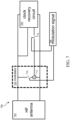
- Fig. 5 shows another illustrative embodiment of an RFID transponder 500.
- the RFID transponder 500 includes a high-frequency (HF) antenna 502, a clock recovery circuit 504, and a modulator 508 that is controlled by means of a modulation signal 506.
- the modulation signal 506 may be provided by a controller included in the RFID transponder (not shown).
- the modulation signal 506 is provided to a modulation switch 510.
- a parallel path as current divider, having a certain ratio.
- two or more modulation transistors may be provided in parallel or in another configuration.
- a current sensor 518 is configured to sense the current in a path that is parallel to a modulation path of the RFID transponder.
- a parallel path with a switch a serial path without a switch
- a parallel path without a switch a parallel path without a switch
- a serial path with a switch a parallel path with a switch.
- Fig. 5 shows a parallel path with a switch.
- a parallel path may be used that does not contain a switch (not shown). In that case, the switch 512 will not be present.
- the RFID transponder further comprises a controller, said controller being configured to connect and disconnect an output of the current sensor 518 to the clock recovery circuit by means of a first controllable switch.
- Controllable switch 516 shown in Fig. 5 is an example of the first controllable switch.
- the controller is configured to connect and disconnect an antenna terminal to the clock recovery circuit by means of a second controllable switch.
- Controllable switch 514 shown in Fig. 5 is an example of the second controllable switch.
- the sensed current and the residual carrier can be fed to the clock recovery circuit 504 in an alternating manner.
- the modulation signal 506 could be used to control said first and second controllable switches. In this way, the sensed current may be fed nearly immediately to the clock recovery circuit 504 when the modulation starts, and the residual carrier may be fed nearly immediately to the clock recovery circuit 504 when the modulation stops.
- the controller is configured to connect the output of the current sensor 518 to the clock recovery circuit 504 and to disconnect the antenna terminals from the clock recovery circuit 504 when the modulator carries out a modulation of the carrier signal. Furthermore, in a practical and effective implementation according to the invention, the controller is configured to connect the antenna terminal to the clock recovery circuit and to disconnect the output of the current sensor 518 from the clock recovery circuit when the modulator does not carry out a modulation of the carrier signal.
- Fig. 6 shows a further illustrative embodiment of an RFID transponder 600.
- the RFID transponder 600 includes a high-frequency (HF) antenna 602, a clock recovery circuit 604, and a modulator 608 that is controlled by means of a modulation signal 606.
- the modulation signal 606 may be provided by a controller included in the RFID transponder (not shown).
- the modulation signal 606 is provided to a modulation switch 610.
- a current sensor 612 is configured to sense the current in a modulation path of the RFID transponder. This implementation has the advantage that no switching of the signals is required.
- Fig. 6 shows an implementation based on a serial path without a switch (i.e., having no switch in addition to the modulation switch 610).
- Fig. 7 shows a further illustrative embodiment of an RFID transponder 700.
- the RFID transponder 700 includes a high-frequency (HF) antenna 702, a clock recovery circuit 704, and a modulator 708 that is controlled by means of a modulation signal 706.
- the modulation signal 706 may be provided by a controller included in the RFID transponder (not shown).
- the modulation signal 706 is provided to a modulation switch 710.
- a current sensor 712 is configured to sense the current in a modulation path of the RFID transponder. It is noted that Fig. 7 shows an implementation based on a serial path with an additional controllable switch 714.
- an RFID transponder different implementations of an RFID transponder are possible. For instance, single ended implementations and differential implementations may be envisaged for connecting the antenna to the clock recovery circuit. It is noted that the principle of recovering the clock signal using the current sensed by the current sensor can be applied to these different implementations. Furthermore, recovering the clock signal using the current may be implemented in various ways. More specifically, the current sensor data may be converted and input to the clock recovery circuit in various ways, for example by means of a simple current mirror, logarithmic amplifiers, transimpedance amplifiers and other amplifiers.
Landscapes
- Engineering & Computer Science (AREA)
- Computer Networks & Wireless Communication (AREA)
- Computer Hardware Design (AREA)
- Microelectronics & Electronic Packaging (AREA)
- Physics & Mathematics (AREA)
- General Physics & Mathematics (AREA)
- Theoretical Computer Science (AREA)
- Signal Processing (AREA)
- Near-Field Transmission Systems (AREA)
Claims (10)
- RFID-Transponder (Radio Frequency Identification) (100), der einen Modulator (102) und eine Taktwiederherstellungsschaltung (106) umfasst, wobei:der Modulator (102) dazu konfiguriert ist, ein von einem externen RFID-Lesegerät empfangenes unmoduliertes Trägersignal zu modulieren;dadurch gekennzeichnet, dass der RFID-Transponder (100) ferner einen Stromsensor (104) umfasst, der dazu konfiguriert ist, einen Strom zu erfassen, der durch einen oder mehrere in dem Modulator (102) umfassten Transistoren fließt; unddass die Taktwiederherstellungsschaltung (106) dazu konfiguriert ist, ein Taktsignal unter Verwendung des von dem Stromsensor (104) erfassten Stroms wiederherzustellen;wobei die Taktwiederherstellungsschaltung (106) dazu konfiguriert ist, den Strom zum Wiederherstellen des Taktsignals zu verwenden, wenn der Modulator (102) eine Modulation des Trägersignals durchführt;und wobei die Taktwiederherstellungsschaltung (106) dazu konfiguriert ist, das Trägersignal zum Wiederherstellen des Taktsignals zu verwenden, wenn der Modulator (102) eine Modulation des Trägersignals nicht durchführt.
- RFID-Transponder (100) nach Anspruch 1, wobei der Stromsensor (104) dazu konfiguriert ist, den Strom in einem Modulationspfad des RFID-Transponders (100) zu erfassen.
- RFID-Transponder (100) nach Anspruch 1, wobei der Stromsensor (104) dazu konfiguriert ist, den Strom in einem Pfad zu erfassen, der parallel zu einem Modulationspfad des RFID-Transponders (100) ist.
- RFID-Transponder (100) nach einem der vorhergehenden Ansprüche, der ferner eine Steuerung umfasst, wobei die Steuerung dazu konfiguriert ist, einen Ausgang des Stromsensors (104) unter Verwendung eines ersten steuerbaren Schalters mit der Taktwiederherstellungsschaltung (106) zu verbinden bzw. von dieser zu trennen.
- RFID-Transponder (100) nach Anspruch 4, wobei die Steuerung ferner dazu konfiguriert ist, einen Antennenanschluss unter Verwendung eines zweiten steuerbaren Schalters mit der Taktwiederherstellungsschaltung (106) zu verbinden bzw. von dieser zu trennen.
- RFID-Transponder (100) nach Anspruch 4 oder 5, wobei die Steuerung dazu konfiguriert ist, den Ausgang des Stromsensors mit der Taktwiederherstellungsschaltung (106) zu verbinden und den Antennenanschluss von der Taktwiederherstellungsschaltung (106) zu trennen, wenn der Modulator eine Modulation des Trägersignals durchführt.
- RFID-Transponder (100) nach einem der Ansprüche 4 bis 6, wobei die Steuerung dazu konfiguriert ist, den Antennenanschluss mit der Taktwiederherstellungsschaltung (106) zu verbinden und den Ausgang des Stromsensors (104) von der Taktwiederherstellungsschaltung zu trennen, wenn der Modulator (102) eine Modulation des Trägersignals nicht durchführt.
- Verfahren (200) zum Betreiben eines RFID-Transponders (Radio Frequency Identification), wobei der RFID-Transponder einen Modulator und eine Taktwiederherstellungsschaltung umfasst, wobei das Verfahren umfasst:Modulieren (202) eines unmodulierten Trägersignals, das von einem externen RFID-Lesegerät empfangen wird, durch den Modulator;dadurch gekennzeichnet, dass das Verfahren ferner das Erfassen (204) eines Stroms durch einen im RFID-Transponder enthaltenen Stromsensor umfasst, der durch einen oder mehrere im Modulator umfasste Transistoren fließt; undWiederherstellen (206) eines Taktsignals durch die Taktwiederherstellungsschaltung unter Verwendung des vom Stromsensor erfassten Stroms;wobei die Taktwiederherstellungsschaltung den Strom zum Wiederherstellen des Taktsignals verwendet, wenn der Modulator eine Modulation des Trägersignals durchführt;und wobei die Taktwiederherstellungsschaltung das Trägersignal zum Wiederherstellen des Taktsignals verwendet, wenn der Modulator eine Modulation des Trägersignals nicht durchführt.
- Verfahren (200) nach Anspruch 10, wobei der Stromsensor den Strom in einem Modulationspfad des RFID-Transponders erfasst.
- Verfahren (200) nach Anspruch 10, wobei der Stromsensor den Strom in einem Pfad erfasst, der parallel zu einem Modulationspfad des RFID-Transponders ist.
Priority Applications (3)
| Application Number | Priority Date | Filing Date | Title |
|---|---|---|---|
| EP19203260.5A EP3809329B1 (de) | 2019-10-15 | 2019-10-15 | Taktwiederherstellung in einem rfid-transponder |
| US17/024,055 US11206058B2 (en) | 2019-10-15 | 2020-09-17 | Clock recovery in an RFID transponder |
| CN202011087741.XA CN112668351A (zh) | 2019-10-15 | 2020-10-12 | Rfid应答器中的时钟恢复 |
Applications Claiming Priority (1)
| Application Number | Priority Date | Filing Date | Title |
|---|---|---|---|
| EP19203260.5A EP3809329B1 (de) | 2019-10-15 | 2019-10-15 | Taktwiederherstellung in einem rfid-transponder |
Publications (2)
| Publication Number | Publication Date |
|---|---|
| EP3809329A1 EP3809329A1 (de) | 2021-04-21 |
| EP3809329B1 true EP3809329B1 (de) | 2024-08-14 |
Family
ID=68281038
Family Applications (1)
| Application Number | Title | Priority Date | Filing Date |
|---|---|---|---|
| EP19203260.5A Active EP3809329B1 (de) | 2019-10-15 | 2019-10-15 | Taktwiederherstellung in einem rfid-transponder |
Country Status (3)
| Country | Link |
|---|---|
| US (1) | US11206058B2 (de) |
| EP (1) | EP3809329B1 (de) |
| CN (1) | CN112668351A (de) |
Families Citing this family (2)
| Publication number | Priority date | Publication date | Assignee | Title |
|---|---|---|---|---|
| EP3703269B1 (de) * | 2019-02-26 | 2022-06-08 | Nxp B.V. | Phasenabgleich eines steuergerätetakts mit einem feld |
| US12132816B2 (en) | 2022-09-30 | 2024-10-29 | Nxp B.V. | Method and integrated circuit for clock recovery in an RFID tag |
Citations (1)
| Publication number | Priority date | Publication date | Assignee | Title |
|---|---|---|---|---|
| EP1986136B1 (de) * | 2007-04-26 | 2010-09-29 | EM Microelectronic-Marin SA | Transponderschaltung mit doppelter Taktableitungseinheit |
Family Cites Families (13)
| Publication number | Priority date | Publication date | Assignee | Title |
|---|---|---|---|---|
| US7027786B1 (en) | 1998-10-21 | 2006-04-11 | Parkervision, Inc. | Carrier and clock recovery using universal frequency translation |
| AU2003211094A1 (en) | 2002-02-15 | 2003-09-09 | Quellan, Inc. | Multi-level signal clock recovery technique |
| CN101038617B (zh) | 2006-03-17 | 2010-07-21 | 上海华虹集成电路有限责任公司 | 用于非接触式ic卡和射频识别标签芯片的时钟恢复电路 |
| US20100085158A1 (en) * | 2007-01-09 | 2010-04-08 | Nxp, B.V. | Method of transmitting data, electronic device and transponder |
| DE102007017534B4 (de) * | 2007-04-13 | 2017-11-16 | Infineon Technologies Austria Ag | Transponderschaltungsanordnung nebst zugehörigem Transponder und Verfahren zum Bereitstellen einer Vorsorgungsspannung |
| US8059478B2 (en) * | 2008-12-04 | 2011-11-15 | Kovio, Inc. | Low cost testing and sorting for integrated circuits |
| US7940073B1 (en) * | 2008-12-05 | 2011-05-10 | Kovio, Inc. | Deactivation of integrated circuits |
| JP5494252B2 (ja) | 2009-09-11 | 2014-05-14 | ソニー株式会社 | 同期発振器、クロック再生装置、クロック分配回路、およびマルチモード注入回路 |
| WO2012009791A1 (en) * | 2010-07-19 | 2012-01-26 | Risst Ltd. | Fingerprint sensors and systems incorporating fingerprint sensors |
| EP2697745B1 (de) * | 2011-04-15 | 2025-01-01 | Thales Dis France SAS | Verfahren, schaltung und vorrichtung zur kontaktlosen kommunikation mit aktivierter übertragung |
| EP2535838A1 (de) * | 2011-06-16 | 2012-12-19 | Gemalto SA | Kontaktloses Kommunikationsverfahren mit negativer Modulation |
| KR102013402B1 (ko) * | 2012-08-13 | 2019-08-22 | 삼성전자주식회사 | Rfid 장치 |
| BR102015002248A8 (pt) * | 2015-01-30 | 2022-11-29 | Centro Nac De Tecnologia Eletronica Avancada S A | Transponder com modulação de carga de até 100% |
-
2019
- 2019-10-15 EP EP19203260.5A patent/EP3809329B1/de active Active
-
2020
- 2020-09-17 US US17/024,055 patent/US11206058B2/en not_active Expired - Fee Related
- 2020-10-12 CN CN202011087741.XA patent/CN112668351A/zh not_active Withdrawn
Patent Citations (1)
| Publication number | Priority date | Publication date | Assignee | Title |
|---|---|---|---|---|
| EP1986136B1 (de) * | 2007-04-26 | 2010-09-29 | EM Microelectronic-Marin SA | Transponderschaltung mit doppelter Taktableitungseinheit |
Also Published As
| Publication number | Publication date |
|---|---|
| EP3809329A1 (de) | 2021-04-21 |
| US11206058B2 (en) | 2021-12-21 |
| US20210111758A1 (en) | 2021-04-15 |
| CN112668351A (zh) | 2021-04-16 |
Similar Documents
| Publication | Publication Date | Title |
|---|---|---|
| US5889273A (en) | Wireless communication data storing medium for receiving a plurality of carriers of proximate frequencies and a transmission/receiving method | |
| US11423239B2 (en) | Integrated circuits and methods for protocol detection and decoding in near field communications | |
| US10282953B2 (en) | Electronic tamper detection device | |
| US20100073138A1 (en) | RFID tag communication system and RFID tag communication apparatus | |
| EP2701314B1 (de) | Detektion von NFC lastmodulierten Signalen | |
| KR102883342B1 (ko) | Nfc 트랜시버를 위한 클럭 복원 회로, nfc 트랜시버, 및 nfc 트랜시버의 제어 방법 | |
| EP1486903B1 (de) | Lese-/Schreibevorrichtung zur Herstellung einer effizienten Sendung/Empfang mit einem batterielosen Datenträger | |
| EP3809329B1 (de) | Taktwiederherstellung in einem rfid-transponder | |
| US6525649B1 (en) | Non-contact communication system and interrogator used therefor | |
| US7714727B2 (en) | RFID antenna design that can selectively enable and disable the antenna | |
| US11270177B2 (en) | RFID transponder and corresponding operating method | |
| EP3742341B1 (de) | Rfid-transponder und verfahren zum betrieb davon | |
| US11126906B2 (en) | Transponder and corresponding operating method | |
| JP2006303970A (ja) | 非接触式通信システム | |
| US12348343B2 (en) | Method and device for detecting proximity of an external RF field during ongoing RF activity of the device | |
| JP2009271775A (ja) | 受信装置 | |
| JP2006344228A (ja) | Icカードリーダ | |
| JP2012208825A (ja) | 受信回路、受信装置及び受信信号処理方法 | |
| CN100397416C (zh) | 具有用于评估自同步信号信息的信号评估装置的无源数据载体 | |
| KR20260033378A (ko) | Fdt 카운팅 회로 및 이를 포함하는 근거리 무선 통신 카드 |
Legal Events
| Date | Code | Title | Description |
|---|---|---|---|
| PUAI | Public reference made under article 153(3) epc to a published international application that has entered the european phase |
Free format text: ORIGINAL CODE: 0009012 |
|
| STAA | Information on the status of an ep patent application or granted ep patent |
Free format text: STATUS: THE APPLICATION HAS BEEN PUBLISHED |
|
| AK | Designated contracting states |
Kind code of ref document: A1 Designated state(s): AL AT BE BG CH CY CZ DE DK EE ES FI FR GB GR HR HU IE IS IT LI LT LU LV MC MK MT NL NO PL PT RO RS SE SI SK SM TR |
|
| AX | Request for extension of the european patent |
Extension state: BA ME |
|
| STAA | Information on the status of an ep patent application or granted ep patent |
Free format text: STATUS: REQUEST FOR EXAMINATION WAS MADE |
|
| 17P | Request for examination filed |
Effective date: 20211021 |
|
| RBV | Designated contracting states (corrected) |
Designated state(s): AL AT BE BG CH CY CZ DE DK EE ES FI FR GB GR HR HU IE IS IT LI LT LU LV MC MK MT NL NO PL PT RO RS SE SI SK SM TR |
|
| STAA | Information on the status of an ep patent application or granted ep patent |
Free format text: STATUS: EXAMINATION IS IN PROGRESS |
|
| 17Q | First examination report despatched |
Effective date: 20230228 |
|
| GRAP | Despatch of communication of intention to grant a patent |
Free format text: ORIGINAL CODE: EPIDOSNIGR1 |
|
| STAA | Information on the status of an ep patent application or granted ep patent |
Free format text: STATUS: GRANT OF PATENT IS INTENDED |
|
| INTG | Intention to grant announced |
Effective date: 20240510 |
|
| GRAS | Grant fee paid |
Free format text: ORIGINAL CODE: EPIDOSNIGR3 |
|
| GRAA | (expected) grant |
Free format text: ORIGINAL CODE: 0009210 |
|
| STAA | Information on the status of an ep patent application or granted ep patent |
Free format text: STATUS: THE PATENT HAS BEEN GRANTED |
|
| AK | Designated contracting states |
Kind code of ref document: B1 Designated state(s): AL AT BE BG CH CY CZ DE DK EE ES FI FR GB GR HR HU IE IS IT LI LT LU LV MC MK MT NL NO PL PT RO RS SE SI SK SM TR |
|
| REG | Reference to a national code |
Ref country code: GB Ref legal event code: FG4D |
|
| REG | Reference to a national code |
Ref country code: CH Ref legal event code: EP |
|
| REG | Reference to a national code |
Ref country code: DE Ref legal event code: R096 Ref document number: 602019056913 Country of ref document: DE |
|
| REG | Reference to a national code |
Ref country code: IE Ref legal event code: FG4D |
|
| PGFP | Annual fee paid to national office [announced via postgrant information from national office to epo] |
Ref country code: FR Payment date: 20240919 Year of fee payment: 6 |
|
| REG | Reference to a national code |
Ref country code: LT Ref legal event code: MG9D |
|
| REG | Reference to a national code |
Ref country code: NL Ref legal event code: MP Effective date: 20240814 |
|
| PGFP | Annual fee paid to national office [announced via postgrant information from national office to epo] |
Ref country code: DE Payment date: 20240919 Year of fee payment: 6 |
|
| PG25 | Lapsed in a contracting state [announced via postgrant information from national office to epo] |
Ref country code: NO Free format text: LAPSE BECAUSE OF FAILURE TO SUBMIT A TRANSLATION OF THE DESCRIPTION OR TO PAY THE FEE WITHIN THE PRESCRIBED TIME-LIMIT Effective date: 20241114 |
|
| REG | Reference to a national code |
Ref country code: AT Ref legal event code: MK05 Ref document number: 1713989 Country of ref document: AT Kind code of ref document: T Effective date: 20240814 |
|
| PG25 | Lapsed in a contracting state [announced via postgrant information from national office to epo] |
Ref country code: NL Free format text: LAPSE BECAUSE OF FAILURE TO SUBMIT A TRANSLATION OF THE DESCRIPTION OR TO PAY THE FEE WITHIN THE PRESCRIBED TIME-LIMIT Effective date: 20240814 Ref country code: PT Free format text: LAPSE BECAUSE OF FAILURE TO SUBMIT A TRANSLATION OF THE DESCRIPTION OR TO PAY THE FEE WITHIN THE PRESCRIBED TIME-LIMIT Effective date: 20241216 Ref country code: FI Free format text: LAPSE BECAUSE OF FAILURE TO SUBMIT A TRANSLATION OF THE DESCRIPTION OR TO PAY THE FEE WITHIN THE PRESCRIBED TIME-LIMIT Effective date: 20240814 Ref country code: GR Free format text: LAPSE BECAUSE OF FAILURE TO SUBMIT A TRANSLATION OF THE DESCRIPTION OR TO PAY THE FEE WITHIN THE PRESCRIBED TIME-LIMIT Effective date: 20241115 Ref country code: PL Free format text: LAPSE BECAUSE OF FAILURE TO SUBMIT A TRANSLATION OF THE DESCRIPTION OR TO PAY THE FEE WITHIN THE PRESCRIBED TIME-LIMIT Effective date: 20240814 |
|
| PG25 | Lapsed in a contracting state [announced via postgrant information from national office to epo] |
Ref country code: BG Free format text: LAPSE BECAUSE OF FAILURE TO SUBMIT A TRANSLATION OF THE DESCRIPTION OR TO PAY THE FEE WITHIN THE PRESCRIBED TIME-LIMIT Effective date: 20240814 |
|
| PG25 | Lapsed in a contracting state [announced via postgrant information from national office to epo] |
Ref country code: LV Free format text: LAPSE BECAUSE OF FAILURE TO SUBMIT A TRANSLATION OF THE DESCRIPTION OR TO PAY THE FEE WITHIN THE PRESCRIBED TIME-LIMIT Effective date: 20240814 |
|
| PG25 | Lapsed in a contracting state [announced via postgrant information from national office to epo] |
Ref country code: IS Free format text: LAPSE BECAUSE OF FAILURE TO SUBMIT A TRANSLATION OF THE DESCRIPTION OR TO PAY THE FEE WITHIN THE PRESCRIBED TIME-LIMIT Effective date: 20241214 Ref country code: AT Free format text: LAPSE BECAUSE OF FAILURE TO SUBMIT A TRANSLATION OF THE DESCRIPTION OR TO PAY THE FEE WITHIN THE PRESCRIBED TIME-LIMIT Effective date: 20240814 |
|
| PG25 | Lapsed in a contracting state [announced via postgrant information from national office to epo] |
Ref country code: HR Free format text: LAPSE BECAUSE OF FAILURE TO SUBMIT A TRANSLATION OF THE DESCRIPTION OR TO PAY THE FEE WITHIN THE PRESCRIBED TIME-LIMIT Effective date: 20240814 |
|
| PG25 | Lapsed in a contracting state [announced via postgrant information from national office to epo] |
Ref country code: RS Free format text: LAPSE BECAUSE OF FAILURE TO SUBMIT A TRANSLATION OF THE DESCRIPTION OR TO PAY THE FEE WITHIN THE PRESCRIBED TIME-LIMIT Effective date: 20241114 Ref country code: ES Free format text: LAPSE BECAUSE OF FAILURE TO SUBMIT A TRANSLATION OF THE DESCRIPTION OR TO PAY THE FEE WITHIN THE PRESCRIBED TIME-LIMIT Effective date: 20240814 |
|
| PG25 | Lapsed in a contracting state [announced via postgrant information from national office to epo] |
Ref country code: RS Free format text: LAPSE BECAUSE OF FAILURE TO SUBMIT A TRANSLATION OF THE DESCRIPTION OR TO PAY THE FEE WITHIN THE PRESCRIBED TIME-LIMIT Effective date: 20241114 Ref country code: PT Free format text: LAPSE BECAUSE OF FAILURE TO SUBMIT A TRANSLATION OF THE DESCRIPTION OR TO PAY THE FEE WITHIN THE PRESCRIBED TIME-LIMIT Effective date: 20241216 Ref country code: PL Free format text: LAPSE BECAUSE OF FAILURE TO SUBMIT A TRANSLATION OF THE DESCRIPTION OR TO PAY THE FEE WITHIN THE PRESCRIBED TIME-LIMIT Effective date: 20240814 Ref country code: NO Free format text: LAPSE BECAUSE OF FAILURE TO SUBMIT A TRANSLATION OF THE DESCRIPTION OR TO PAY THE FEE WITHIN THE PRESCRIBED TIME-LIMIT Effective date: 20241114 Ref country code: NL Free format text: LAPSE BECAUSE OF FAILURE TO SUBMIT A TRANSLATION OF THE DESCRIPTION OR TO PAY THE FEE WITHIN THE PRESCRIBED TIME-LIMIT Effective date: 20240814 Ref country code: LV Free format text: LAPSE BECAUSE OF FAILURE TO SUBMIT A TRANSLATION OF THE DESCRIPTION OR TO PAY THE FEE WITHIN THE PRESCRIBED TIME-LIMIT Effective date: 20240814 Ref country code: IS Free format text: LAPSE BECAUSE OF FAILURE TO SUBMIT A TRANSLATION OF THE DESCRIPTION OR TO PAY THE FEE WITHIN THE PRESCRIBED TIME-LIMIT Effective date: 20241214 Ref country code: HR Free format text: LAPSE BECAUSE OF FAILURE TO SUBMIT A TRANSLATION OF THE DESCRIPTION OR TO PAY THE FEE WITHIN THE PRESCRIBED TIME-LIMIT Effective date: 20240814 Ref country code: GR Free format text: LAPSE BECAUSE OF FAILURE TO SUBMIT A TRANSLATION OF THE DESCRIPTION OR TO PAY THE FEE WITHIN THE PRESCRIBED TIME-LIMIT Effective date: 20241115 Ref country code: FI Free format text: LAPSE BECAUSE OF FAILURE TO SUBMIT A TRANSLATION OF THE DESCRIPTION OR TO PAY THE FEE WITHIN THE PRESCRIBED TIME-LIMIT Effective date: 20240814 Ref country code: ES Free format text: LAPSE BECAUSE OF FAILURE TO SUBMIT A TRANSLATION OF THE DESCRIPTION OR TO PAY THE FEE WITHIN THE PRESCRIBED TIME-LIMIT Effective date: 20240814 Ref country code: BG Free format text: LAPSE BECAUSE OF FAILURE TO SUBMIT A TRANSLATION OF THE DESCRIPTION OR TO PAY THE FEE WITHIN THE PRESCRIBED TIME-LIMIT Effective date: 20240814 Ref country code: AT Free format text: LAPSE BECAUSE OF FAILURE TO SUBMIT A TRANSLATION OF THE DESCRIPTION OR TO PAY THE FEE WITHIN THE PRESCRIBED TIME-LIMIT Effective date: 20240814 |
|
| PG25 | Lapsed in a contracting state [announced via postgrant information from national office to epo] |
Ref country code: DK Free format text: LAPSE BECAUSE OF FAILURE TO SUBMIT A TRANSLATION OF THE DESCRIPTION OR TO PAY THE FEE WITHIN THE PRESCRIBED TIME-LIMIT Effective date: 20240814 Ref country code: RO Free format text: LAPSE BECAUSE OF FAILURE TO SUBMIT A TRANSLATION OF THE DESCRIPTION OR TO PAY THE FEE WITHIN THE PRESCRIBED TIME-LIMIT Effective date: 20240814 Ref country code: SM Free format text: LAPSE BECAUSE OF FAILURE TO SUBMIT A TRANSLATION OF THE DESCRIPTION OR TO PAY THE FEE WITHIN THE PRESCRIBED TIME-LIMIT Effective date: 20240814 |
|
| PG25 | Lapsed in a contracting state [announced via postgrant information from national office to epo] |
Ref country code: EE Free format text: LAPSE BECAUSE OF FAILURE TO SUBMIT A TRANSLATION OF THE DESCRIPTION OR TO PAY THE FEE WITHIN THE PRESCRIBED TIME-LIMIT Effective date: 20240814 |
|
| PG25 | Lapsed in a contracting state [announced via postgrant information from national office to epo] |
Ref country code: CZ Free format text: LAPSE BECAUSE OF FAILURE TO SUBMIT A TRANSLATION OF THE DESCRIPTION OR TO PAY THE FEE WITHIN THE PRESCRIBED TIME-LIMIT Effective date: 20240814 |
|
| PG25 | Lapsed in a contracting state [announced via postgrant information from national office to epo] |
Ref country code: IT Free format text: LAPSE BECAUSE OF FAILURE TO SUBMIT A TRANSLATION OF THE DESCRIPTION OR TO PAY THE FEE WITHIN THE PRESCRIBED TIME-LIMIT Effective date: 20240814 Ref country code: SK Free format text: LAPSE BECAUSE OF FAILURE TO SUBMIT A TRANSLATION OF THE DESCRIPTION OR TO PAY THE FEE WITHIN THE PRESCRIBED TIME-LIMIT Effective date: 20240814 |
|
| REG | Reference to a national code |
Ref country code: DE Ref legal event code: R097 Ref document number: 602019056913 Country of ref document: DE |
|
| REG | Reference to a national code |
Ref country code: CH Ref legal event code: PL |
|
| PLBE | No opposition filed within time limit |
Free format text: ORIGINAL CODE: 0009261 |
|
| STAA | Information on the status of an ep patent application or granted ep patent |
Free format text: STATUS: NO OPPOSITION FILED WITHIN TIME LIMIT |
|
| PG25 | Lapsed in a contracting state [announced via postgrant information from national office to epo] |
Ref country code: MC Free format text: LAPSE BECAUSE OF FAILURE TO SUBMIT A TRANSLATION OF THE DESCRIPTION OR TO PAY THE FEE WITHIN THE PRESCRIBED TIME-LIMIT Effective date: 20240814 |
|
| PG25 | Lapsed in a contracting state [announced via postgrant information from national office to epo] |
Ref country code: LU Free format text: LAPSE BECAUSE OF NON-PAYMENT OF DUE FEES Effective date: 20241015 Ref country code: BE Free format text: LAPSE BECAUSE OF NON-PAYMENT OF DUE FEES Effective date: 20241031 |
|
| 26N | No opposition filed |
Effective date: 20250515 |
|
| GBPC | Gb: european patent ceased through non-payment of renewal fee |
Effective date: 20241114 |
|
| PG25 | Lapsed in a contracting state [announced via postgrant information from national office to epo] |
Ref country code: CH Free format text: LAPSE BECAUSE OF NON-PAYMENT OF DUE FEES Effective date: 20241031 |
|
| P01 | Opt-out of the competence of the unified patent court (upc) registered |
Free format text: CASE NUMBER: APP_29880/2025 Effective date: 20250623 |
|
| REG | Reference to a national code |
Ref country code: BE Ref legal event code: MM Effective date: 20241031 |
|
| PG25 | Lapsed in a contracting state [announced via postgrant information from national office to epo] |
Ref country code: SE Free format text: LAPSE BECAUSE OF FAILURE TO SUBMIT A TRANSLATION OF THE DESCRIPTION OR TO PAY THE FEE WITHIN THE PRESCRIBED TIME-LIMIT Effective date: 20240814 |
|
| PG25 | Lapsed in a contracting state [announced via postgrant information from national office to epo] |
Ref country code: GB Free format text: LAPSE BECAUSE OF NON-PAYMENT OF DUE FEES Effective date: 20241114 |
|
| PG25 | Lapsed in a contracting state [announced via postgrant information from national office to epo] |
Ref country code: IE Free format text: LAPSE BECAUSE OF NON-PAYMENT OF DUE FEES Effective date: 20241015 |
|
| PG25 | Lapsed in a contracting state [announced via postgrant information from national office to epo] |
Ref country code: CY Free format text: LAPSE BECAUSE OF FAILURE TO SUBMIT A TRANSLATION OF THE DESCRIPTION OR TO PAY THE FEE WITHIN THE PRESCRIBED TIME-LIMIT; INVALID AB INITIO Effective date: 20191015 |
|
| PG25 | Lapsed in a contracting state [announced via postgrant information from national office to epo] |
Ref country code: HU Free format text: LAPSE BECAUSE OF FAILURE TO SUBMIT A TRANSLATION OF THE DESCRIPTION OR TO PAY THE FEE WITHIN THE PRESCRIBED TIME-LIMIT; INVALID AB INITIO Effective date: 20191015 |