EP3812955B1 - Fingerabdruckdetektor und elektronische vorrichtung - Google Patents
Fingerabdruckdetektor und elektronische vorrichtung Download PDFInfo
- Publication number
- EP3812955B1 EP3812955B1 EP19808956.7A EP19808956A EP3812955B1 EP 3812955 B1 EP3812955 B1 EP 3812955B1 EP 19808956 A EP19808956 A EP 19808956A EP 3812955 B1 EP3812955 B1 EP 3812955B1
- Authority
- EP
- European Patent Office
- Prior art keywords
- chip
- fingerprint
- mcu
- chip set
- optical
- Prior art date
- Legal status (The legal status is an assumption and is not a legal conclusion. Google has not performed a legal analysis and makes no representation as to the accuracy of the status listed.)
- Active
Links
Images

Classifications
-
- G—PHYSICS
- G06—COMPUTING OR CALCULATING; COUNTING
- G06F—ELECTRIC DIGITAL DATA PROCESSING
- G06F1/00—Details not covered by groups G06F3/00 - G06F13/00 and G06F21/00
- G06F1/26—Power supply means, e.g. regulation thereof
- G06F1/32—Means for saving power
- G06F1/3203—Power management, i.e. event-based initiation of a power-saving mode
- G06F1/3206—Monitoring of events, devices or parameters that trigger a change in power modality
- G06F1/3215—Monitoring of peripheral devices
-
- G—PHYSICS
- G06—COMPUTING OR CALCULATING; COUNTING
- G06F—ELECTRIC DIGITAL DATA PROCESSING
- G06F1/00—Details not covered by groups G06F3/00 - G06F13/00 and G06F21/00
- G06F1/16—Constructional details or arrangements
- G06F1/1613—Constructional details or arrangements for portable computers
- G06F1/1626—Constructional details or arrangements for portable computers with a single-body enclosure integrating a flat display, e.g. Personal Digital Assistants [PDAs]
-
- G—PHYSICS
- G06—COMPUTING OR CALCULATING; COUNTING
- G06F—ELECTRIC DIGITAL DATA PROCESSING
- G06F1/00—Details not covered by groups G06F3/00 - G06F13/00 and G06F21/00
- G06F1/16—Constructional details or arrangements
- G06F1/1613—Constructional details or arrangements for portable computers
- G06F1/1633—Constructional details or arrangements of portable computers not specific to the type of enclosures covered by groups G06F1/1615 - G06F1/1626
- G06F1/1684—Constructional details or arrangements related to integrated I/O peripherals not covered by groups G06F1/1635 - G06F1/1675
-
- G—PHYSICS
- G06—COMPUTING OR CALCULATING; COUNTING
- G06F—ELECTRIC DIGITAL DATA PROCESSING
- G06F1/00—Details not covered by groups G06F3/00 - G06F13/00 and G06F21/00
- G06F1/26—Power supply means, e.g. regulation thereof
- G06F1/32—Means for saving power
- G06F1/3203—Power management, i.e. event-based initiation of a power-saving mode
- G06F1/3206—Monitoring of events, devices or parameters that trigger a change in power modality
- G06F1/3231—Monitoring the presence, absence or movement of users
-
- G—PHYSICS
- G06—COMPUTING OR CALCULATING; COUNTING
- G06F—ELECTRIC DIGITAL DATA PROCESSING
- G06F1/00—Details not covered by groups G06F3/00 - G06F13/00 and G06F21/00
- G06F1/26—Power supply means, e.g. regulation thereof
- G06F1/32—Means for saving power
- G06F1/3203—Power management, i.e. event-based initiation of a power-saving mode
- G06F1/3234—Power saving characterised by the action undertaken
- G06F1/3243—Power saving in microcontroller unit
-
- G—PHYSICS
- G06—COMPUTING OR CALCULATING; COUNTING
- G06F—ELECTRIC DIGITAL DATA PROCESSING
- G06F1/00—Details not covered by groups G06F3/00 - G06F13/00 and G06F21/00
- G06F1/26—Power supply means, e.g. regulation thereof
- G06F1/32—Means for saving power
- G06F1/3203—Power management, i.e. event-based initiation of a power-saving mode
- G06F1/3234—Power saving characterised by the action undertaken
- G06F1/325—Power saving in peripheral device
-
- G—PHYSICS
- G06—COMPUTING OR CALCULATING; COUNTING
- G06F—ELECTRIC DIGITAL DATA PROCESSING
- G06F1/00—Details not covered by groups G06F3/00 - G06F13/00 and G06F21/00
- G06F1/26—Power supply means, e.g. regulation thereof
- G06F1/32—Means for saving power
- G06F1/3203—Power management, i.e. event-based initiation of a power-saving mode
- G06F1/3234—Power saving characterised by the action undertaken
- G06F1/3287—Power saving characterised by the action undertaken by switching off individual functional units in the computer system
-
- G—PHYSICS
- G06—COMPUTING OR CALCULATING; COUNTING
- G06V—IMAGE OR VIDEO RECOGNITION OR UNDERSTANDING
- G06V10/00—Arrangements for image or video recognition or understanding
- G06V10/10—Image acquisition
- G06V10/12—Details of acquisition arrangements; Constructional details thereof
- G06V10/14—Optical characteristics of the device performing the acquisition or on the illumination arrangements
- G06V10/145—Illumination specially adapted for pattern recognition, e.g. using gratings
-
- G—PHYSICS
- G06—COMPUTING OR CALCULATING; COUNTING
- G06V—IMAGE OR VIDEO RECOGNITION OR UNDERSTANDING
- G06V10/00—Arrangements for image or video recognition or understanding
- G06V10/10—Image acquisition
- G06V10/12—Details of acquisition arrangements; Constructional details thereof
- G06V10/14—Optical characteristics of the device performing the acquisition or on the illumination arrangements
- G06V10/147—Details of sensors, e.g. sensor lenses
-
- G—PHYSICS
- G06—COMPUTING OR CALCULATING; COUNTING
- G06V—IMAGE OR VIDEO RECOGNITION OR UNDERSTANDING
- G06V40/00—Recognition of biometric, human-related or animal-related patterns in image or video data
- G06V40/10—Human or animal bodies, e.g. vehicle occupants or pedestrians; Body parts, e.g. hands
- G06V40/12—Fingerprints or palmprints
- G06V40/13—Sensors therefor
- G06V40/1318—Sensors therefor using electro-optical elements or layers, e.g. electroluminescent sensing
-
- G—PHYSICS
- G06—COMPUTING OR CALCULATING; COUNTING
- G06V—IMAGE OR VIDEO RECOGNITION OR UNDERSTANDING
- G06V40/00—Recognition of biometric, human-related or animal-related patterns in image or video data
- G06V40/10—Human or animal bodies, e.g. vehicle occupants or pedestrians; Body parts, e.g. hands
- G06V40/12—Fingerprints or palmprints
- G06V40/1365—Matching; Classification
-
- Y—GENERAL TAGGING OF NEW TECHNOLOGICAL DEVELOPMENTS; GENERAL TAGGING OF CROSS-SECTIONAL TECHNOLOGIES SPANNING OVER SEVERAL SECTIONS OF THE IPC; TECHNICAL SUBJECTS COVERED BY FORMER USPC CROSS-REFERENCE ART COLLECTIONS [XRACs] AND DIGESTS
- Y02—TECHNOLOGIES OR APPLICATIONS FOR MITIGATION OR ADAPTATION AGAINST CLIMATE CHANGE
- Y02D—CLIMATE CHANGE MITIGATION TECHNOLOGIES IN INFORMATION AND COMMUNICATION TECHNOLOGIES [ICT], I.E. INFORMATION AND COMMUNICATION TECHNOLOGIES AIMING AT THE REDUCTION OF THEIR OWN ENERGY USE
- Y02D10/00—Energy efficient computing, e.g. low power processors, power management or thermal management
Definitions
- the present application relates to the field of fingerprint identification, and more particularly, to an apparatus for fingerprint detection and an electronic device.
- Optical under-screen fingerprint identification technology refers that an optical fingerprint module captures an optical signal formed by reflection or transmittance of light by a finger. Since the optical signal carries fingerprint information of the finger, under-screen fingerprint identification is realized.
- the optical fingerprint module may include multiple sensor chips to realize large area fingerprint detection. However, this leads to increases in corresponding devices and traces, which increases structural complexity of the optical fingerprint module and increases power consumption as well.
- CN 109 416 739 A discloses a multi-sensor-based under-screen fingerprint capturing method and system, where the method is applied to an under-screen fingerprint capturing system including multiple fingerprint sensors, and includes: acquiring fingerprint information of a user captured by the multiple fingerprint sensors, where each fingerprint sensor corresponds to a sensing region, and sensing regions corresponding to the multiple fingerprint sensors form a fingerprint capturing region of the under-screen fingerprint capturing system; and determining an effectively pressed fingerprint sensor among the multiple fingerprint sensors according to the fingerprint information of the user, where the fingerprint information of the user captured by the effectively pressed fingerprint sensor is used for fingerprint authentication of the user.
- Embodiments of the present application provide an apparatus for fingerprint detection and an electronic device.
- the apparatus has lower structural complexity.
- an apparatus for fingerprint detection where the apparatus is disposed under a display screen of an electronic device to implement under-screen optical fingerprint detection, and includes a sensor chip array with at least three fingerprint sensor and an MCU, the sensor chip array includes a first chip set in which chips use a multiplexed first signal line and a second chip set in which chips use a multiplexed second signal line, where the chips in the first chip set and the chips in the second chip set are alternately arranged in each row and each column of the sensor chip array, and the MCU is configured to: control one first chip in the first chip set to perform fingerprint detection on a finger on the display screen at a time, where the first chip communicates with the MCU by using the first signal line; and, control one second chip in the second chip set to perform fingerprint detection on the finger at the time, where the second chip communicates with the MCU by using the second signal line.
- a fingerprint sensor chip array in a fingerprint detection apparatus is divided into two chip sets; and chips in the two chip sets are alternately arranged in each row and each column of the sensor chip array. In this way, probability that a finger is simultaneously pressed above two chips in the same chip set is lower. Therefore, by setting each of chips in each chip set to multiplex one signal line, and controlling only one chip in the same chip set to perform fingerprint detection at a time, a trace in a fingerprint detection apparatus could be reduced, so that the fingerprint detection apparatus is more compact in structure and power consumption is also saved by avoiding simultaneous working of a large number of sensor chips.
- the first signal line and the second signal line are configured to transmit fingerprint data and control signal, wherein the control signal comprise a clock signal and/or a reset signal.
- the first chip set and the second chip set communicate with the MCU by any one of the following communication methods: serial peripheral interface (SPI) communication, universal asynchronous transceiver and transmitter (UART) communication, and inter integrated circuit (I2C) communication.
- SPI serial peripheral interface
- UART universal asynchronous transceiver and transmitter
- I2C inter integrated circuit
- each chip in the sensor chip array uses a separate signal line to perform transmission of a chip selection (CS) signal and an interrupt (INT) signal with the MCU.
- CS chip selection
- INT interrupt
- the MCU is configured to: receive an instruction sent by a processor of the electronic device, and control, based on the instruction, the first chip and/or the second chip to perform fingerprint detection at the time.
- power supplies of each chip in the first chip set share a power capacitor and/or the powers for a same functional module of each chip shares a power capacitor; and power supplies of each chip in the second chip set share a power capacitor and/or the powers for a same functional module of each chip shares a power capacitor; where the same function module on the different chips refers to the circuit module that achieves the same function in the fingerprint detection process.
- the power for the same functional module includes: an analog power for the same functional module and/or a digital power for the same functional module.
- the power capacitor is a decoupling capacitor.
- an electronic device including a display screen, a processor, and the apparatus for fingerprint detection according to the first aspect or any possible implementation manner of the first aspect, or the apparatus for fingerprint detection according to the second aspect or any possible implementation manner of the second aspect.
- the processor is connected to an MCU to control a sensor chip array in the chip in the second chip set shares a power capacitor and/or a power for a same functional module of each chip shares a power capacitor
- the same function module refers to the circuit module that achieves same function in the fingerprint detection process, where sensor chips in the first chip set and sensor chips in the second chip set are alternately arranged in each row and each column of the sensor chip array
- the MCU is configured to: control one first chip in the first chip set to perform fingerprint detection on a finger on the display screen at a time, wherein the first chip is connected to the power capacitor; and/or, control one second chip in the second chip set to perform fingerprint detection on the finger at the time, wherein the second chip is connected to the power capacitor.
- a fingerprint sensor chip array in a fingerprint detection apparatus is divided into two chip sets; and chips in the two chip sets are alternately arranged in each row and each column of the sensor chip array. In this way, probability that a finger is simultaneously pressed above two chips in the same chip set is lower. Therefore, by setting multiple chips in one chip set to share a power capacitor, and controlling only one chip in the same chip set to perform fingerprint detection at an apparatus through the MCU to perform fingerprint detection.
- embodiments of the present application may be applied to a fingerprint system, including but not limited to an optical, ultrasonic or other fingerprint identification system and a medical diagnostic product based on optical, ultrasonic or other fingerprint imaging.
- a fingerprint system including but not limited to an optical, ultrasonic or other fingerprint identification system and a medical diagnostic product based on optical, ultrasonic or other fingerprint imaging.
- the embodiments of the present application are only described by an example of an optical fingerprint system, which should not constitute any limitation to the embodiments of the present application, and the embodiments of the present application are also applicable to other systems using an optical, ultrasonic or other imaging technology or the like.
- the optical fingerprint system provided in an embodiment of the present application may be applied to a smart phone, a tablet computer, and other mobile terminals having a display screen or other electronic devices. More specifically, in the foregoing electronic device, an optical fingerprint module may be disposed in a partial region or an entire region under a display screen, thereby forming an under-display optical fingerprint system. Alternatively, the optical fingerprint module may be partially or entirely integrated into the interior of the display screen of the electronic device to form an in-display optical fingerprint system.
- Optical under-screen fingerprint identification technology uses light returned from a top surface of a display component of a device for fingerprint sensing and other sensing operations.
- the returned light carries information of an object such as a finger in contact with the top surface, and optical fingerprint detection of a particular optical sensor module located under a display screen is implemented by capturing and detecting the returned light by the finger.
- An optical sensor module can be designed to achieve a desired optical imaging by properly configuring optical elements for capturing and detecting the returned light.
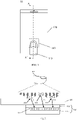
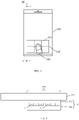
- FIG. 1 and FIG. 3 are schematic diagrams of an electronic device to which the present application is applicable.
- FIG. 1 and FIG. 3 are schematic oriented diagrams of an electronic device 10; and
- FIG. 2 and FIG. 4 are partial schematic cross-sectional diagrams of the electronic device 10 shown in FIG 1 and FIG. 3 taken along an A-A' direction, respectively.
- the electronic device 10 includes a display screen 120 and an optical fingerprint module 130.
- the optical fingerprint module 130 is disposed in a partial region under the display screen 120.
- the optical fingerprint module 130 includes an optical fingerprint sensor 134 that includes a sensing array 133 having a plurality of optical sensing units 131 (which may also be referred to as pixels, photosensitive pixels, pixel units, etc.).
- a region where the sensing array 133 is located or a sensing region of the sensing array 133 is a fingerprint detecting region 103 of the optical fingerprint module 130. As shown in FIG. 1 , the fingerprint detecting region 103 is located within a display region of the display screen 120.
- the optical fingerprint module 130 may also be disposed at other positions, such as a side of the display screen 120 or an edge non-light transmitting region of the electronic device 10, and an optical signal from at least part of the display region of the display screen 120 is directed to the optical fingerprint module 130 through a light path design, such that the fingerprint detecting region 103 is actually located in the display region of the display screen 120.
- an area of the fingerprint detecting region 103 may be different from an area of the sensing array 133 of the optical fingerprint module 130.
- the area of the fingerprint detecting region 103 of the optical fingerprint module 130 is larger than the area of the sensing array 133 of the optical fingerprint module 130 through a light path design such as lens imaging, reflective folding, or light convergence or reflection, etc.
- the area of the fingerprint detecting region 103 of the optical fingerprint module 130 may also be designed to be substantially identical with the area of the sensing array 133 of the optical fingerprint module 130.
- a fingerprint input can be implemented merely by pressing a finger on the fingerprint detecting region 103 in the display screen 120. Since fingerprint detection may be implemented in the screen, there is no need to exclusively reserve space for a front surface of the electronic device 10 adopting the foregoing structure to set a fingerprint button (such as a Home button), so that a full screen solution may be adopted; that is, the display region of the display screen 120 may be substantially extended to an entire front surface of the electronic device 10.
- a fingerprint button such as a Home button
- the optical fingerprint module 130 includes a light detecting portion 134 and an optical component 132.
- the light detecting portion 134 includes the sensing array 133 and a readout circuit and other auxiliary circuits electrically connected to the sensing array 133, and may be fabricated on a die by a semiconductor process, to form an optical fingerprint chip or an optical fingerprint sensor 134, which is also referred to as a sensor chip or a chip, etc.
- the sensing array 133 is specifically a photodetector array including a plurality of photo detectors distributed in an array, and the photo detectors may serve as the optical sensing units as described above.
- the optical component 132 may be disposed above the sensing array 133 of the light detecting portion 134, and may specifically include a filter layer, a light directing layer or a light path directing structure, and other optical elements.
- the filter layer may be used to filter ambient light passing through a finger, and the light directing layer is mainly used to direct reflected light reflected from a finger surface to the sensing array 133 for optical detection.
- the optical component 132 and the light detecting portion 134 may be encapsulated in the same optical fingerprint member.
- the optical component 132 and the light detecting portion 134 may be encapsulated in the same optical fingerprint chip, or the optical component 132 may be disposed outside a chip where the light detecting portion 134 is located, for example, the optical component 132 is attached above the chip, or a part of elements of the optical component 132 are integrated into the chip.
- the light directing layer of the optical component 132 may be specifically a collimator layer fabricated on a semiconductor silicon wafer and having a plurality of collimating units or micro-pore arrays, and the collimating units may be specifically a hole.
- Light in the reflected light reflected from the finger that is vertically incident on the collimating unit may pass through the collimating unit and be received by the optical sensing unit below the collimating unit, and light with an excessively large incident angle is attenuated through multiple reflection inside the collimating unit. Therefore, each optical sensing unit may substantially only receive the reflected light reflected from a fingerprint pattern right above the optical sensing unit, and thus the sensing array 133 may detect a fingerprint image of the finger.
- the light directing layer may also be an optical lens layer having one or more lens units, for example, a lens group composed of one or more aspheric lenses, for converging reflected light reflected from a finger to the sensing array 133 of the light detecting portion 134 below the optical lens layer, so that the sensing array 133 may perform imaging based on the reflected light so as to obtain a fingerprint image of the finger.
- the optical lens layer may be provided with a pinhole in a light path of the lens unit(s), and the pinhole may cooperate with the optical lens layer to expand a field of view of the optical fingerprint module 130, to improve a fingerprint imaging effect of the optical fingerprint module 130.
- the light directing layer may also specifically adopt a micro-lens layer
- the micro-lens layer has a micro-lens array constituted by a plurality of micro-lenses, and may be formed above the sensing array 133 of the light detecting portion 134 by a semiconductor growth process or other processes, and each micro-lens may correspond to one of the sensing units in the sensing array 133 respectively.
- Other optical film layers such as a dielectric layer or a passivation layer may be formed between the micro-lens layer and the sensing unit.
- a light blocking layer (or referred to as a light shielding layer, a light resisting layer, etc.) having a micro-pore may also be formed between the micro-lens layer and the sensing unit, where the micro-pore is formed between the corresponding micro-lens and the sensing unit, and the light blocking layer may block optical interference between adjacent micro-lenses and the sensing units, such that light corresponding to the sensing unit is converged to the interior of the micro-pore through the micro-lens and is transmitted to the sensing unit via the micro-pore to perform optical fingerprint imaging.
- a micro-lens layer may be further disposed above or below the collimator layer or the optical lens layer.
- the collimator layer or the optical lens layer is used in combination with the micro-lens layer, the specific laminated structure or light path may require to be adjusted according to actual needs.
- the display screen 120 may adopt a display screen with a self-emitting display unit, for example, an organic light-emitting diode (OLED) display screen or a micro light-emitting diode (Micro-LED) display screen.
- OLED organic light-emitting diode
- Micro-LED micro light-emitting diode
- the optical fingerprint module 130 may use a display unit (that is, an OLED light source) of the OLED display screen 120 located at the fingerprint detecting region 103 as an excitation light source for optical fingerprint detection.
- the display screen 120 When a finger 140 is pressed against the fingerprint detecting region 103, the display screen 120 emits a beam of light 111 to a finger 140 above the fingerprint detecting region 103, and the light 111 is reflected by a surface of the finger 140 to form reflected light or form scattered light after scattering inside the finger 140.
- the reflected light and scattered light are also collectively referred to as reflected light for convenience of description. Since a ridge 141 and a valley 142 of a fingerprint have different light reflecting abilities, reflected light 151 from the ridge of the fingerprint and reflected light 152 from the valley of the fingerprint have different light intensities.
- the reflected light is received by the sensing array 133 in the optical fingerprint module 130 and converted into a corresponding electrical signal, that is, a fingerprint detection signal.
- Fingerprint image data can be obtained based on the fingerprint detection signal, and fingerprint matching verification can be further performed, thereby implementing an optical fingerprint identification function in the electronic device 10.
- the optical fingerprint module 130 may also use an internal light source or an external light source to provide an optical signal for fingerprint detection.
- the optical fingerprint module 130 may be applied to a non-self-emitting display screen, such as a liquid crystal display screen or other passive light-emitting display screens.
- the optical fingerprint system of the electronic device 10 may further include an excitation light source for optical fingerprint detection.
- the excitation light source may specifically be an infrared light source or a light source of non-visible light with a specific wavelength, which may be disposed under the backlight module of the liquid crystal display screen or disposed in an edge region under a protective cover of the electronic device 10.
- the optical fingerprint module 130 may be disposed under the liquid crystal panel or the edge region of the protective cover, and by being directed over a light path, light for fingerprint detection may reach the optical fingerprint module 130.
- the optical fingerprint module 130 may also be disposed under the backlight module, and the backlight module allows the light for fingerprint detection to pass through the liquid crystal panel and the backlight module and reach the optical fingerprint module 130 by providing a via hole on film layers such as a diffusion sheet, a brightening sheet, a reflection sheet or the like, or by performing other optical designs.
- the optical fingerprint module 130 uses an internal light source or an external light source to provide an optical signal for fingerprint detection, a detection principle is consistent with the foregoing description.
- the electronic device 10 may further include a transparent protective cover; and the cover may be a glass cover or a sapphire cover, which is located above the display screen 120 and covers a front surface of the electronic device 10. Therefore, in an embodiment of the present application, the so-called the finger being pressed against the display screen 120 actually refers to the finger being pressed against a cover above the display screen 120 or a surface of a protective layer covering the cover.
- the electronic device 10 may further include a circuit board that is disposed under the optical fingerprint module 130.
- the optical fingerprint module 130 may be bonded to the circuit board by a back adhesive, and achieve electrical connection with the circuit board by welding of a pad and a mental wire.
- the optical fingerprint module 130 may achieve electrical interconnection and signal transmission with other peripheral circuits or other elements of the electronic device 10 through the circuit board.
- the optical fingerprint module 130 may receive a control signal of a processing unit of the electronic device 10 through the circuit board, and may also output a fingerprint detection signal from the optical fingerprint module 130 to the processing unit, a control unit and the like of the electronic device 10 through the circuit board.
- the optical fingerprint module 130 may only include one optical fingerprint sensor 134, and in this case, the fingerprint detecting region 103 of the optical fingerprint module 130 has a smaller area and a fixed position, and therefore, when an fingerprint input is performed, a user needs to press a finger at a specific position of the fingerprint detecting region 103, otherwise the optical fingerprint module 130 may not be able to capture a fingerprint image, thereby resulting in poor user experience.
- the optical fingerprint module 130 may include a plurality of optical fingerprint sensors 134.
- the plurality of optical fingerprint sensors 134 may be disposed under the display screen 120 side by side in a splicing manner, and sensing regions of the plurality of optical fingerprint sensors 134 collectively constitute the fingerprint detecting region 103 of the optical fingerprint module 130.
- the fingerprint detecting region 103 of the optical fingerprint module 130 may be extended to a main region of a lower half part of the display screen, that is, to a customary pressing region of a finger, thereby implementing a blind-press type of fingerprint input operation.
- the fingerprint detecting region 103 may also be extended to a half of the display region or even the entire display region, thereby achieving half-screen or full-screen fingerprint detection.
- an optical fingerprint module 130 in the electronic device 10 includes a plurality of optical fingerprint sensors 134, and the plurality of optical fingerprint sensors 134 may be disposed under a display screen 120 side by side in a splicing manner or the like for example, and sensing regions of the plurality of optical fingerprint sensors 134 collectively constitute a fingerprint detecting region 103 of the optical fingerprint module 130.
- an optical component 132 may include a plurality of light directing layers, with each light directing layer corresponding to one optical fingerprint sensor and attached to be disposed above the corresponding optical fingerprint sensor, respectively.
- the plurality of optical fingerprint sensors 134 may also share an integral light directing layer, i.e., the light directing layer has a sufficiently large area to cover sensing arrays of the plurality of optical fingerprint sensors 134.
- the optical component 132 may further include other optical elements, for example, a filter or other optical films, which may be disposed between the light directing layer and the optical fingerprint sensor, or between the display screen 120 and the light directing layer, for mainly isolating the influence of external interference light on optical fingerprint detection.
- the filter may be used to filter out ambient light that penetrates a finger and enters into the optical fingerprint sensors 134 via the display screen 120. Similar to the light directing layer, the filter may be separately provided for each of the optical fingerprint sensors 134 to filter interference light, or a large-area filter may also be used to simultaneously cover the plurality of optical fingerprint sensors 134.
- the light directing layer may also be replaced by an optical lens, and an aperture may be formed by a light-shielding material on the optical lens to cooperate with the optical lens to converge fingerprint detection light to the optical fingerprint sensor under the optical lens so as to achieve fingerprint imaging.
- each optical fingerprint sensor may be separately configured with an optical lens for fingerprint imaging, or the plurality of optical fingerprint sensors 134 may also utilize the same optical lens to achieve light convergence and fingerprint imaging.
- each of the optical fingerprint sensors 134 may even further have dual sensing arrays or multiple sensing arrays, and two or more optical lenses are simultaneously configured to cooperate with the two or more sensing arrays for optical imaging so as to reduce an imaging distance and enhance an imaging effect.
- the number of optical fingerprint sensors 134 is increased, and therefore communication lines and capacitors associated with the optical fingerprint sensors 134 are also increased, thereby increasing structure complexity of an optical fingerprint module.
- An embodiment of the present application provides a fingerprint detection solution, which can make an optical fingerprint module have a more compact structure.
- the optical fingerprint sensor in the above optical fingerprint module 130 is also referred to as a sensor chip or a chip.
- FIG. 5 is a schematic block diagram of an apparatus 300 for fingerprint detection according to an embodiment of the present application.
- the apparatus 300 is disposed under a display screen of an electronic device to implement under-screen optical fingerprint detection.
- the apparatus 300 includes a sensor chip array 310 and a micro-programmed control unit (MCU) 320.
- the sensor chip array 310 includes a first chip set 311 and a second chip set 312.
- Chips in the first chip set 311 and chips in the second chip set 312 are alternately arranged in each row and each column of the sensor chip array 310.
- the chips in the first chip set 311 multiplex a first signal line 321, and the chips in the second chip set 312 multiplex a second signal line 322.
- the MCU 320 is configured to:
- a fingerprint sensor chip array in a fingerprint detection apparatus is divided into two chip sets, that is, a first chip set and a second chip set. Chips in the two chip sets are alternately arranged in each row and each column of the sensor chip array. In this way, probability that a finger is simultaneously pressed above two chips in the same chip set is lower. Therefore, by setting each of chips in each chip set to multiplex one signal line, and controlling only one chip in the same chip set to perform fingerprint detection at a time, a trace in a fingerprint detection apparatus could be reduced, so that the fingerprint detection apparatus is more compact in structure and power consumption is also saved by avoiding simultaneous working of a large number of sensor chips.
- the sensor chip array 310 may include one or more rows of sensor chips or one or more columns of sensor chips.
- the sensor chip array 310 includes only one row of sensor chips, chips in the first chip set 311 and chips in the second chip set 312 are alternately arranged in the row of the sensor chips.
- chips in the first chip set 311 and chips in the second chip set 312 are alternately arranged in the column of the sensor chips.
- FIG. 6 illustrates several possible fingerprint detecting regions.
- the fingerprint detecting regions include a plurality of sub-regions corresponding to a plurality of sensor chips in a sensor chip array 310 respectively, and each of the sensor chips is used to detect a fingerprint in the corresponding sub-region.
- the sensor chip array 310 includes two chips, and a first chip set 311 includes a chip 1 and a second chip set 312 includes a chip 2.
- the sensor chip array 310 includes three chips, and a first chip set 311 includes a chip 1 and a chip 3, and a second chip set 312 includes a chip 2.
- the sensor chip array 310 includes four chips, and a first chip set 311 includes a chip 1 and a chip 3, and a second chip set 312 includes a chip 2 and a chip 4.
- FIG. 6 (a) the sensor chip array 310 includes two chips, and a first chip set 311 includes a chip 1 and a second chip set 312 includes a chip 2.
- the sensor chip array 310 includes six chips, and a first chip set 311 includes a chip 1, a chip 3 and a chip 5, and a second chip set 312 includes a chip 2, a chip 4 and a chip 6. As shown in FIG. 6 (f) , the sensor chip array 310 includes eight chips, and a first chip set 311 includes a chip 1, a chip 3, a chip 6 and a chip 8 and a second chip set 312 includes a chip 2, a chip 4, a chip 5 and a chip 7.
- non-adjacent chips or chips in diagonal positions belong to the same chip set.
- the non-adjacent chip 1 and chip 3 are used as the first chip set 311, and non-adjacent chip 2 and chip 4 are used as the second chip set 312.
- the first chip set 311 and the second chip set 312 can work in parallel, but only one chip in the same chip set is controlled to perform fingerprint detection each time.
- the chip 1 and the chip 2 can simultaneously detect an optical signal returned by the finger, but at this time, the chip 3 in the first chip set 311 and the chip 4 in the second chip set do not work.
- the chip 2 and the chip 3 can simultaneously detect an optical signal returned by the finger, but while the chip 2 and the chip 3 are working, the remaining chips in the first chip set 311 and the second chip set 312 do not work.
- the chip 5 and the chip 6 can simultaneously detect an optical signal returned by the finger, but while the chip 5 and the chip 6 are working, the remaining chips in the first chip set 311 and the second chip set 312 do not work.
- the number, size, and arrangement of the fingerprint sensor chips shown above are only examples, and can be adjusted according to actual needs.
- the number of chips in the sensor chip array may further be other values, and the sensor chip array may be square or circular.
- the MCU 320 may be connected to a host, and the host includes a processor of an electronic device such as a master control of the electronic device.
- the MCU 320 may receive an instruction sent by the master control of the electronic device, and control, according to the instruction, one first chip in the first chip set 311 and/or one second chip in the second chip set 312 to perform fingerprint detection on the finger at the time.
- the host is bridged by the MCU 320 to manage communication of the sensor chip array 310.
- the master control of the electronic device can obtain pressing information of the finger from a touch panel, such as a pressing region and a pressing position of the finger, and determine which sensor chip of the chip set needs to be used to perform fingerprint detection on the finger according to the pressing information.
- the master control of the electronic device may send an instruction to the MCU 320 to instruct a certain sensor chip to perform fingerprint detection on the finger. After receiving the instruction, the MCU 320 sends the instruction to the sensor chip through the corresponding signal line, so that the sensor chip performs fingerprint detection on the finger after receiving the instruction.
- the chips in the first chip set 311 multiplex a first signal line 321, and the chips in the second chip set 312 multiplex a second signal line 322.
- the first signal line 321 and the second signal line 322 may be configured to transmit at least one of fingerprint data (DATA), a clock signal (CLOCK), a reset signal (RESET) and other signals for example.
- the clock signal is used for signal reception and transmission synchronization.
- the sensor chip needs to send captured fingerprint data to the MCU 320 according to the received clock signal so as to avoid an error code.
- the fingerprint data is data obtained by simply processing an optical signal returned by a finger captured by the sensor chip, and the data carries fingerprint information of the finger.
- the reset signal is used for restoring the sensor chip to an initial state.
- each chip in the sensor chip array 310 may use a separate signal line to perform transmission of the CS signal and the INT signal with the MCU 320.
- the chip selection signal may be used for selecting a particular chip in each chip set for fingerprint detection.
- the first signal line 321 is used only for one first chip in the first chip set 311 to communicate with the MCU 320 each time.
- the second signal line 322 is used only for one second chip in the second chip set 312 to communicate with MCU 320 each time. That is, the first chip and the second chip may communicate with the MCU 320 simultaneously by using the first signal line 321 and the second signal line 322, respectively, but other chips in the first chip set 311 do not communicate with the MCU 320 by using the first signal line 321 simultaneously with the first chip, and other chips in the second chip set 312 do not communicate with the MCU 320 by using the second signal line 322 simultaneously with the second chip.
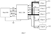
- a host 100 is bridged by an MCU 320 to manage each chip in a sensor chip array 310.
- the MCU 320 is connected to chips such as a chip 1, a chip 3, and the like that are not adjacent or diagonally located in a first chip set 311 through a first signal line 321, and the MCU 320 is connected to chips such as a chip 2, a chip 4, and the like that are not adjacent or diagonally located in a second chip set 312 through a second signal line 322.
- the first signal line 321 and the second signal line 322 are configured to transmit fingerprint data, a clock signal, a reset signal, and the like acquired by a chip of the corresponding chip set, respectively.
- the MCU 320 is connected to the chip 1, the chip 2, the chip 3, the chip 4, ..., and a chip N through a signal line 1, a signal line 2, a signal line 3, a signal line 4, ..., and a signal line ⁇ ,N, respectively, and the signal line 1, the signal line 2, the signal line 3, the signal line 4, ..., and the signal line ⁇ ,N are configured to transmit chip selection signals and interrupt signals of the chip 1, the chip 2, the chip 3, the chip 4, ..., and the chip N, respectively.
- only one chip of the first chip set 311 is working to perform signal transmission with the MCU 320 by using the first signal line 321.
- only one chip of the second chip set 312 is working to perform signal transmission with the MCU 320 by using the second signal line 322.
- the host 100 transmits chip selection (CS) signals to the chip 1 and the chip 2 through the MCU 320, and the chip selection signals of the chip 1 and the chip 2 are transmitted to the chip 1 and the chip 2 through the signal line 1 and the signal line 2, respectively.
- the chip 1 and the chip 2 are turned on to perform fingerprint detection on the finger, so as to acquire fingerprint data, and send interrupts (INT) to the host 100 by the MCU 320 through the signal line 1 and the signal line 2, respectively, to notify the host 100 to take the fingerprint data.
- CS chip selection
- INT interrupts
- the fingerprint data acquired by the chip 1 and the chip 2 may be transmitted to the MCU 320 through the first signal line 321 and the second signal line 322, respectively, and further transmitted to the host 100.
- reset (RESET) signals may be sent to the chip 1 and the chip 2 by the MCU 320 through the first signal line 321 and the second signal line 322, respectively, so that the chip 1 and the chip 2 are restored to an initial state.
- the sensor chip array 310 may also be controlled by other communication methods to perform fingerprint detection, such as UART communication and I2C communication.
- a power of each chip in the first chip set 311 shares a power capacitor; and a power of each chip in the second chip set shares a power capacitor.
- the MCU 320 is configured to:
- the number of capacitors in a fingerprint detection apparatus could be reduced, so that the fingerprint detection apparatus is more compact in structure and power consumption is also saved by avoiding simultaneous working of a large number of sensor chips.
- the power capacitor may be, for example, a decoupling capacitor, or an uncoupling capacitor.
- the capacitor is connected between a power supply of a chip and the ground, and can be configured to achieve functions of electric energy storage, decoupling, noise reduction, stabilization, buffering, and the like.
- the power capacitor is not limited in the present application. For example, one chip set may also share other bypass capacitors.
- the power of each chip in the first chip set 311 shares a power capacitor, and the power capacitor is used only for one chip in the first chip set 311 each time, but is not electrically conductive with multiple chips in the first chip set 311 simultaneously.
- the power of each chip in the second chip set 312 shares a power capacitor, and the power capacitor is used only for one chip in the second chip set 312 each time, but is not electrically conductive with multiple chips in the second chip set 312 simultaneously.
- the foregoing power of each chip in the same chip set may include, for example, at least one of the following powers: a power supply of each chip in the same chip set, an analog power for the same functional module of each chip in the same chip set, and a digital power for the same functional module of each chip in the same chip set.
- a power supply of each chip in each chip set may share a power capacitor and/or a power for a same functional module of each chip in each chip set may also share a power capacitor.
- a power supply of each chip in the first chip set shares a power capacitor and/or a power for a same functional module of each chip shares a power capacitor; and a power supply of each chip in the second chip set shares a power capacitor and/or a power for a same functional module of each chip shares a power capacitor.
- a power supply of a chip is, for example, an AVDD, which is used for providing total voltage to the chip.
- an AVDD of each chip in each chip set is the same, and may share a power capacitor.
- Voltages required for different functional modules on a chip may be different, and thus powers for the different functional modules of the chip are different.
- the different functional modules on the chip for example, include an analog to digital converter (ADC), a Field Programmable Gain Amplifier (FPGA), a photodiode (PD), and other functional modules.
- ADC analog to digital converter
- FPGA Field Programmable Gain Amplifier
- PD photodiode
- a power for an ADC module of each chip in the same chip set may share a capacitor
- a power for a PD module of each chip in the same chip set may share a capacitor
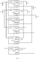
- a first chip set 311 includes a chip 1, a chip 3, ..., and a chip N-1
- a second chip set 312 includes a chip 2, a chip 4, ..., and a chip N.
- An AVDD power of each chip in the first chip set 311 is connected to a capacitor C1
- an AVDD of each chip in the second chip set 312 is connected to a capacitor C2.
- an analog power for each functional module with different voltage requirements can be obtained, such as an ADC, an FPGA, a PD and other functional modules.
- an analog power of each chip for a same functional module and providing a same voltage shares a capacitor.
- FIG. 8 for the sake of brevity, only one analog power is shown in each chip.
- the analog power of each chip in the first chip set 311 is connected to a capacitor C3
- the analog power of each chip in the second chip set 312 is connected to a capacitor C4.
- a digital power of each chip in the first chip set 311 is connected to a capacitor C5
- a digital power of each chip in the second chip set 312 is connected to a capacitor C6.
- the digital power is configured to supply power to various digital logic and input/output (I/O) interfaces.
- Each power of a chip is usually managed by a power management unit (PMU).
- PMU power management unit
- the chip stops working.
- sensor chips sharing a capacitor only a PMU of one of the sensor chips is turned on at a time, while PMUs inside the other sensor chips are all turned off.
- the chip can communicate with a MCU 320 through the first signal line 321 for fingerprint detection; and when a PMU of one chip in the second chip set 312 is turned on, the chip can communicate with the MCU 320 through the second signal line 322 for fingerprint detection.
- the number of power capacitors could be reduced, cost could be reduced, and the structure of an apparatus 300 for fingerprint detection could be made more compact; on the other hand, since only one sensor chip in each chip set is working each time, the method is conductive to saving power consumption.
- the apparatus 300 may simultaneously adopt, for example, a connection manner of multiplexing signal lines shown in FIG. 7 , and a connection manner of sharing a power capacitor as shown in FIG. 8 .
- the chip may use shared capacitor and signal line for fingerprint detection, while the other chips in the chip set do not use the capacitor and the signal line simultaneously.
- An embodiment of the present application further provides an electronic device, and the electronic device includes a display screen, a processor, and the apparatus 300 for fingerprint detection according to the above various embodiments of the present application.
- the processor is connected to an MCU to control a sensor chip array 310 in the apparatus 300 through the MCU to perform fingerprint detection.
- the processor is, for example, a master control of the electronic device, and the MCU is, for example, the aforementioned MCU 320.
- the display screen may be a normal unfolded display screen or a foldable display screen or a flexible display screen.
- the electronic device in the embodiment of the present application may be portable or mobile computing devices such as a terminal device, a mobile phone, a tablet computer, a notebook computer, a desktop computer, a gaming device, an in-vehicle electronic device or a wearable smart device, and other electronic devices such as an electronic database, an automobile and an automated teller machine (ATM).
- the wearable smart device includes a smart watch or smart glasses or the like that is full-featured, large-sized, and can implement a complete or partial function without relying on a smart phone, and various types of smart wristbands, smart jewelry and other devices for physical signs monitoring that only focus on a certain type of application function, and needs to cooperate with other devices such as a smart phone.
Landscapes
- Engineering & Computer Science (AREA)
- Theoretical Computer Science (AREA)
- Physics & Mathematics (AREA)
- General Physics & Mathematics (AREA)
- General Engineering & Computer Science (AREA)
- Human Computer Interaction (AREA)
- Multimedia (AREA)
- Computer Hardware Design (AREA)
- General Health & Medical Sciences (AREA)
- Vascular Medicine (AREA)
- Artificial Intelligence (AREA)
- Computer Vision & Pattern Recognition (AREA)
- Health & Medical Sciences (AREA)
- Computing Systems (AREA)
- Image Input (AREA)
- Measurement Of The Respiration, Hearing Ability, Form, And Blood Characteristics Of Living Organisms (AREA)
Claims (10)
- Vorrichtung zur Fingerabdruckerkennung, wobei die Vorrichtung unter einem Anzeigebildschirm einer elektronischen Einrichtung angeordnet ist, um eine optische Fingerabdruckerkennung unter dem Bildschirm zu implementieren, und ein Sensorchip-Array (310) mit zumindest drei Fingerabdrucksensorchips und eine mikroprogrammierte Steuereinheit, MCU (320), aufweist, das Sensorchip-Array (310) einen ersten Chipsatz (311), in dem Chips eine gemultiplexte erste Signalleitung verwenden, und einen zweiten Chipsatz (312), in dem Chips eine gemultiplexte zweite Signalleitung verwenden, aufweist, wobei die Chips in dem ersten Chipsatz (311) und die Chips in dem zweiten Chipsatz (312) in jeder Zeile und jeder Spalte des Sensorchip-Arrays (310) abwechselnd angeordnet sind, und die MCU (320) dazu ausgebildet ist:einen ersten Chip in dem ersten Chipsatz (311) zu steuern, um eine Fingerabdruckerkennung an einem Finger auf dem Anzeigebildschirm zu einer Zeit durchzuführen, wobei der erste Chip durch Verwendung der MCU (320) mit der ersten Signalleitung kommuniziert; undeinen zweiten Chip in dem zweiten Chipsatz (312) zu steuern, um eine Fingerabdruckerkennung an dem Finger zu der Zeit durchzuführen, wobei der zweite Chip durch Verwendung der zweiten Signalleitung mit der MCU (320) kommuniziert.
- Vorrichtung nach Anspruch 1, wobei die erste Signalleitung und die zweite Signalleitung dazu ausgebildet sind, Fingerabdruckdaten und ein Steuersignal zu senden, wobei das Steuersignal ein Taktsignal und/oder ein Rücksetzsignal aufweist.
- Vorrichtung nach Anspruch 1 oder 2, wobei der erste Chipsatz (311) und der zweite Chipsatz (312) durch eines der folgenden Kommunikationsverfahren mit der MCU (320) kommunizieren:
serielle periphere Schnittstelle, SPI, -Kommunikation, universeller asynchroner Empfänger/Sender, UART, -Kommunikation, und interintegrierte Schaltung, 12C, - Kommunikation. - Vorrichtung nach einem der Ansprüche 1 bis 3, wobei jeder Chip in dem Sensorchip-Array (310) eine separate Signalleitung verwendet, um die Übertragung eines Chipauswahl, CS, -Signals und eines Interrupt, INT, -Signals mit der MCU (320) durchzuführen.
- Vorrichtung nach einem der Ansprüche 1 bis 4, wobei die MCU (320) dazu ausgebildet ist:
eine von einem Prozessor der elektronischen Einrichtung gesendete Anweisung zu empfangen, und den ersten Chip und/oder den zweiten Chip basierend auf der Anweisung zu steuern, um eine Fingerabdruckerkennung zu der Zeit durchzuführen. - Vorrichtung nach einem der Ansprüche 1 bis 5, wobei:sich Leistungsversorgungen eines jeden Chips in dem ersten Chipsatz (311) einen Leistungskondensator teilen und/oder sich die Leistungen für ein gleiches Funktionsmodul eines jeden Chips einen Leistungskondensator teilen,wobei sich das gleiche Funktionsmodul an den verschiedenen Chips auf das Schaltungsmodul bezieht, das in dem Fingerabdruckerkennungsprozess dieselbe Funktion erzielt.
- Vorrichtung nach einem der Ansprüche 1 bis 6, wobei:sich Leistungsversorgungen eines jeden Chips in dem zweiten Chipsatz (312) einen Leistungskondensator teilen und/oder sich die Leistungen für ein gleiches Funktionsmodul eines jeden Chips einen Leistungskondensator teilen,wobei sich das gleiche Funktionsmodul an den verschiedenen Chips auf das Schaltungsmodul bezieht, das in dem Fingerabdruckerkennungsprozess dieselbe Funktion erzielt.
- Vorrichtung nach Anspruch 6 oder 7, wobei die Leistung für dasselbe Funktionsmodul aufweist:
eine analoge Leistung für dasselbe Funktionsmodul und/oder eine digitale Leistung für dasselbe Funktionsmodul. - Vorrichtung nach einem der Ansprüche 6 bis 8, wobei der Leistungskondensator ein Entkopplungskondensator ist.
- Elektronische Einrichtung, die einen Anzeigebildschirm, einen Prozessor und die Vorrichtung zur Fingerabdruckerkennung nach einem der Ansprüche 1 bis 9 aufweist, wobei der Prozessor mit einer mikroprogrammierten Steuereinheit, MCU, (320) verbunden ist, um ein Sensorchip-Array (310) in der Vorrichtung durch die MCU (320) zu steuern, um eine Fingerabdruckerkennung durchzuführen.
Applications Claiming Priority (1)
| Application Number | Priority Date | Filing Date | Title |
|---|---|---|---|
| PCT/CN2019/103120 WO2021035583A1 (zh) | 2019-08-28 | 2019-08-28 | 指纹检测的装置和电子设备 |
Publications (3)
| Publication Number | Publication Date |
|---|---|
| EP3812955A4 EP3812955A4 (de) | 2021-04-28 |
| EP3812955A1 EP3812955A1 (de) | 2021-04-28 |
| EP3812955B1 true EP3812955B1 (de) | 2022-07-06 |
Family
ID=71172645
Family Applications (1)
| Application Number | Title | Priority Date | Filing Date |
|---|---|---|---|
| EP19808956.7A Active EP3812955B1 (de) | 2019-08-28 | 2019-08-28 | Fingerabdruckdetektor und elektronische vorrichtung |
Country Status (4)
| Country | Link |
|---|---|
| US (1) | US11194985B2 (de) |
| EP (1) | EP3812955B1 (de) |
| CN (1) | CN111325142B (de) |
| WO (1) | WO2021035583A1 (de) |
Families Citing this family (4)
| Publication number | Priority date | Publication date | Assignee | Title |
|---|---|---|---|---|
| CN110867165B (zh) * | 2019-11-29 | 2021-10-15 | 厦门天马微电子有限公司 | 一种显示面板及显示装置 |
| WO2022056860A1 (zh) * | 2020-09-18 | 2022-03-24 | 深圳市汇顶科技股份有限公司 | 触控芯片、打码方法和电子设备 |
| CN113361418B (zh) * | 2021-06-09 | 2025-08-29 | 北京集创北方科技股份有限公司 | 电容式指纹检测装置及终端设备 |
| CN119291458A (zh) * | 2024-10-12 | 2025-01-10 | 南方电网数字电网研究院股份有限公司 | 一种用于芯片运行过程的检测方法及系统 |
Family Cites Families (18)
| Publication number | Priority date | Publication date | Assignee | Title |
|---|---|---|---|---|
| US5859420A (en) * | 1996-02-12 | 1999-01-12 | Dew Engineering And Development Limited | Optical imaging device |
| US6953923B2 (en) | 2003-02-18 | 2005-10-11 | Omnivision Technologies, Inc. | CMOS image sensor having reduced numbers of column readout circuits |
| US7400797B2 (en) * | 2004-10-06 | 2008-07-15 | Corning Incorporated | Transverse closed-loop resonator |
| JP2009038112A (ja) | 2007-07-31 | 2009-02-19 | Toshiba Corp | プリント配線板構造および電子機器 |
| CN104318210B (zh) * | 2014-10-13 | 2017-11-24 | 上海思立微电子科技有限公司 | 一种指纹识别传感器及指纹检测方法 |
| CN104966061B (zh) * | 2015-06-16 | 2018-07-10 | 京东方科技集团股份有限公司 | 一种掌纹识别方法及装置、智能安全门 |
| US10410037B2 (en) * | 2015-06-18 | 2019-09-10 | Shenzhen GOODIX Technology Co., Ltd. | Under-screen optical sensor module for on-screen fingerprint sensing implementing imaging lens, extra illumination or optical collimator array |
| CN106796658A (zh) * | 2016-11-21 | 2017-05-31 | 深圳市汇顶科技股份有限公司 | 指纹传感器及电子终端 |
| EP3438798B1 (de) * | 2017-05-05 | 2020-08-19 | Shenzhen Goodix Technology Co., Ltd. | Fingerabdruckmodul und mobiles endgerät |
| CN107589576B (zh) | 2017-09-30 | 2020-11-06 | 武汉华星光电技术有限公司 | 阵列基板及其制作方法、触控显示面板 |
| CN109726618A (zh) | 2017-10-31 | 2019-05-07 | 深圳芯启航科技有限公司 | 用于传感器的阵列电路及智能手机 |
| CN108899336B (zh) * | 2018-08-22 | 2024-04-30 | 苏州多感科技有限公司 | 一种信号识别系统及其制备方法、电子设备 |
| WO2020056771A1 (zh) * | 2018-09-21 | 2020-03-26 | 深圳市汇顶科技股份有限公司 | 指纹识别装置和电子设备 |
| WO2020061760A1 (zh) * | 2018-09-25 | 2020-04-02 | 深圳市汇顶科技股份有限公司 | 基于多传感器的屏下指纹采集方法、系统和电子设备 |
| CN109358706B (zh) * | 2018-10-30 | 2021-09-28 | 厦门天马微电子有限公司 | 显示面板和显示装置 |
| CN208903234U (zh) * | 2018-11-20 | 2019-05-24 | Oppo广东移动通信有限公司 | 触摸屏及电子设备 |
| CN109637367B (zh) | 2018-12-28 | 2020-12-18 | 厦门天马微电子有限公司 | 显示面板和显示装置 |
| WO2020150888A1 (zh) * | 2019-01-22 | 2020-07-30 | 深圳市汇顶科技股份有限公司 | 指纹识别装置和电子设备 |
-
2019
- 2019-08-28 WO PCT/CN2019/103120 patent/WO2021035583A1/zh not_active Ceased
- 2019-08-28 EP EP19808956.7A patent/EP3812955B1/de active Active
- 2019-11-26 US US16/697,148 patent/US11194985B2/en active Active
-
2020
- 2020-02-18 CN CN202010099891.6A patent/CN111325142B/zh active Active
Also Published As
| Publication number | Publication date |
|---|---|
| US11194985B2 (en) | 2021-12-07 |
| EP3812955A4 (de) | 2021-04-28 |
| WO2021035583A1 (zh) | 2021-03-04 |
| EP3812955A1 (de) | 2021-04-28 |
| US20210064844A1 (en) | 2021-03-04 |
| CN111325142B (zh) | 2023-09-05 |
| CN111325142A (zh) | 2020-06-23 |
Similar Documents
| Publication | Publication Date | Title |
|---|---|---|
| US11232317B2 (en) | Fingerprint identification apparatus and electronic device | |
| CN113343829B (zh) | 指纹识别装置和电子设备 | |
| US11361583B2 (en) | Fingerprint identification apparatus and electronic device | |
| US11194985B2 (en) | Apparatus for fingerprint detection and electronic device | |
| EP3706036A1 (de) | Vorrichtung zur fingerabdruckidentifizierung und elektronische vorrichtung | |
| EP3739508B1 (de) | Vorrichtung zur fingerabdruckidentifizierung und elektronische vorrichtung | |
| EP3889828B1 (de) | Fingerabdruckerkennungseinrichtung und elektronische vorrichtung | |
| EP3647995A1 (de) | Elektronische vorrichtung für fingerabdruckidentifikation | |
| US20200265205A1 (en) | Method and apparatus for fingerprint identification and terminal device | |
| CN211349383U (zh) | 指纹识别的装置和电子设备 | |
| CN111837132B (zh) | 指纹检测的装置和电子设备 | |
| CN111837130A (zh) | 指纹识别装置、背光模组、液晶显示屏和电子设备 | |
| EP3789913A1 (de) | Fingerabdruckerkennungsgerät und elektronische vorrichtung | |
| CN210605736U (zh) | 指纹检测的装置、显示屏和电子设备 | |
| CN210864756U (zh) | 光学指纹装置和电子设备 | |
| CN111133442B (zh) | 指纹检测的装置和电子设备 | |
| US11132523B2 (en) | Method and apparatus for fingerprint identification and electronic device | |
| CN210295124U (zh) | 指纹检测的装置和电子设备 | |
| CN110309820B (zh) | 指纹检测的装置和电子设备 | |
| CN211529180U (zh) | 指纹检测装置和电子设备 | |
| CN212135456U (zh) | 指纹识别的装置和电子设备 | |
| WO2021056425A1 (zh) | 滤光片、指纹检测的装置和电子设备 | |
| CN111095271A (zh) | 指纹检测的装置、显示屏和电子设备 | |
| CN110709859A (zh) | 指纹检测的方法、装置和电子设备 | |
| CN111868736A (zh) | 带有倾斜接收光学元件的显示模块下的指纹传感器 |
Legal Events
| Date | Code | Title | Description |
|---|---|---|---|
| STAA | Information on the status of an ep patent application or granted ep patent |
Free format text: STATUS: UNKNOWN |
|
| STAA | Information on the status of an ep patent application or granted ep patent |
Free format text: STATUS: THE INTERNATIONAL PUBLICATION HAS BEEN MADE |
|
| PUAI | Public reference made under article 153(3) epc to a published international application that has entered the european phase |
Free format text: ORIGINAL CODE: 0009012 |
|
| STAA | Information on the status of an ep patent application or granted ep patent |
Free format text: STATUS: REQUEST FOR EXAMINATION WAS MADE |
|
| 17P | Request for examination filed |
Effective date: 20191204 |
|
| A4 | Supplementary search report drawn up and despatched |
Effective date: 20210202 |
|
| AK | Designated contracting states |
Kind code of ref document: A1 Designated state(s): AL AT BE BG CH CY CZ DE DK EE ES FI FR GB GR HR HU IE IS IT LI LT LU LV MC MK MT NL NO PL PT RO RS SE SI SK SM TR |
|
| AX | Request for extension of the european patent |
Extension state: BA ME |
|
| RIN1 | Information on inventor provided before grant (corrected) |
Inventor name: XIE, HAO Inventor name: ZHANG, JIANYANG |
|
| STAA | Information on the status of an ep patent application or granted ep patent |
Free format text: STATUS: EXAMINATION IS IN PROGRESS |
|
| 17Q | First examination report despatched |
Effective date: 20210929 |
|
| REG | Reference to a national code |
Ref country code: DE Ref legal event code: R079 Ref document number: 602019016817 Country of ref document: DE Free format text: PREVIOUS MAIN CLASS: G06K0009000000 Ipc: G06V0040130000 |
|
| GRAP | Despatch of communication of intention to grant a patent |
Free format text: ORIGINAL CODE: EPIDOSNIGR1 |
|
| STAA | Information on the status of an ep patent application or granted ep patent |
Free format text: STATUS: GRANT OF PATENT IS INTENDED |
|
| RIC1 | Information provided on ipc code assigned before grant |
Ipc: G06F 1/3215 20190101ALI20220330BHEP Ipc: G06F 1/3234 20190101ALI20220330BHEP Ipc: G06F 1/3231 20190101ALI20220330BHEP Ipc: G06F 1/3287 20190101ALI20220330BHEP Ipc: G06F 1/16 20060101ALI20220330BHEP Ipc: G06V 40/13 20220101AFI20220330BHEP |
|
| DAV | Request for validation of the european patent (deleted) | ||
| DAX | Request for extension of the european patent (deleted) | ||
| INTG | Intention to grant announced |
Effective date: 20220426 |
|
| GRAS | Grant fee paid |
Free format text: ORIGINAL CODE: EPIDOSNIGR3 |
|
| GRAA | (expected) grant |
Free format text: ORIGINAL CODE: 0009210 |
|
| STAA | Information on the status of an ep patent application or granted ep patent |
Free format text: STATUS: THE PATENT HAS BEEN GRANTED |
|
| AK | Designated contracting states |
Kind code of ref document: B1 Designated state(s): AL AT BE BG CH CY CZ DE DK EE ES FI FR GB GR HR HU IE IS IT LI LT LU LV MC MK MT NL NO PL PT RO RS SE SI SK SM TR |
|
| REG | Reference to a national code |
Ref country code: AT Ref legal event code: REF Ref document number: 1503411 Country of ref document: AT Kind code of ref document: T Effective date: 20220715 Ref country code: CH Ref legal event code: EP |
|
| REG | Reference to a national code |
Ref country code: DE Ref legal event code: R096 Ref document number: 602019016817 Country of ref document: DE |
|
| REG | Reference to a national code |
Ref country code: IE Ref legal event code: FG4D |
|
| REG | Reference to a national code |
Ref country code: LT Ref legal event code: MG9D |
|
| REG | Reference to a national code |
Ref country code: NL Ref legal event code: MP Effective date: 20220706 |
|
| PG25 | Lapsed in a contracting state [announced via postgrant information from national office to epo] |
Ref country code: SE Free format text: LAPSE BECAUSE OF FAILURE TO SUBMIT A TRANSLATION OF THE DESCRIPTION OR TO PAY THE FEE WITHIN THE PRESCRIBED TIME-LIMIT Effective date: 20220706 Ref country code: RS Free format text: LAPSE BECAUSE OF FAILURE TO SUBMIT A TRANSLATION OF THE DESCRIPTION OR TO PAY THE FEE WITHIN THE PRESCRIBED TIME-LIMIT Effective date: 20220706 Ref country code: PT Free format text: LAPSE BECAUSE OF FAILURE TO SUBMIT A TRANSLATION OF THE DESCRIPTION OR TO PAY THE FEE WITHIN THE PRESCRIBED TIME-LIMIT Effective date: 20221107 Ref country code: NO Free format text: LAPSE BECAUSE OF FAILURE TO SUBMIT A TRANSLATION OF THE DESCRIPTION OR TO PAY THE FEE WITHIN THE PRESCRIBED TIME-LIMIT Effective date: 20221006 Ref country code: NL Free format text: LAPSE BECAUSE OF FAILURE TO SUBMIT A TRANSLATION OF THE DESCRIPTION OR TO PAY THE FEE WITHIN THE PRESCRIBED TIME-LIMIT Effective date: 20220706 Ref country code: LV Free format text: LAPSE BECAUSE OF FAILURE TO SUBMIT A TRANSLATION OF THE DESCRIPTION OR TO PAY THE FEE WITHIN THE PRESCRIBED TIME-LIMIT Effective date: 20220706 Ref country code: LT Free format text: LAPSE BECAUSE OF FAILURE TO SUBMIT A TRANSLATION OF THE DESCRIPTION OR TO PAY THE FEE WITHIN THE PRESCRIBED TIME-LIMIT Effective date: 20220706 Ref country code: FI Free format text: LAPSE BECAUSE OF FAILURE TO SUBMIT A TRANSLATION OF THE DESCRIPTION OR TO PAY THE FEE WITHIN THE PRESCRIBED TIME-LIMIT Effective date: 20220706 Ref country code: ES Free format text: LAPSE BECAUSE OF FAILURE TO SUBMIT A TRANSLATION OF THE DESCRIPTION OR TO PAY THE FEE WITHIN THE PRESCRIBED TIME-LIMIT Effective date: 20220706 |
|
| REG | Reference to a national code |
Ref country code: AT Ref legal event code: MK05 Ref document number: 1503411 Country of ref document: AT Kind code of ref document: T Effective date: 20220706 |
|
| PG25 | Lapsed in a contracting state [announced via postgrant information from national office to epo] |
Ref country code: PL Free format text: LAPSE BECAUSE OF FAILURE TO SUBMIT A TRANSLATION OF THE DESCRIPTION OR TO PAY THE FEE WITHIN THE PRESCRIBED TIME-LIMIT Effective date: 20220706 Ref country code: IS Free format text: LAPSE BECAUSE OF FAILURE TO SUBMIT A TRANSLATION OF THE DESCRIPTION OR TO PAY THE FEE WITHIN THE PRESCRIBED TIME-LIMIT Effective date: 20221106 Ref country code: HR Free format text: LAPSE BECAUSE OF FAILURE TO SUBMIT A TRANSLATION OF THE DESCRIPTION OR TO PAY THE FEE WITHIN THE PRESCRIBED TIME-LIMIT Effective date: 20220706 Ref country code: GR Free format text: LAPSE BECAUSE OF FAILURE TO SUBMIT A TRANSLATION OF THE DESCRIPTION OR TO PAY THE FEE WITHIN THE PRESCRIBED TIME-LIMIT Effective date: 20221007 |
|
| REG | Reference to a national code |
Ref country code: CH Ref legal event code: PL |
|
| REG | Reference to a national code |
Ref country code: DE Ref legal event code: R097 Ref document number: 602019016817 Country of ref document: DE |
|
| PG25 | Lapsed in a contracting state [announced via postgrant information from national office to epo] |
Ref country code: SM Free format text: LAPSE BECAUSE OF FAILURE TO SUBMIT A TRANSLATION OF THE DESCRIPTION OR TO PAY THE FEE WITHIN THE PRESCRIBED TIME-LIMIT Effective date: 20220706 Ref country code: RO Free format text: LAPSE BECAUSE OF FAILURE TO SUBMIT A TRANSLATION OF THE DESCRIPTION OR TO PAY THE FEE WITHIN THE PRESCRIBED TIME-LIMIT Effective date: 20220706 Ref country code: MC Free format text: LAPSE BECAUSE OF FAILURE TO SUBMIT A TRANSLATION OF THE DESCRIPTION OR TO PAY THE FEE WITHIN THE PRESCRIBED TIME-LIMIT Effective date: 20220706 Ref country code: LU Free format text: LAPSE BECAUSE OF NON-PAYMENT OF DUE FEES Effective date: 20220828 Ref country code: LI Free format text: LAPSE BECAUSE OF NON-PAYMENT OF DUE FEES Effective date: 20220831 Ref country code: DK Free format text: LAPSE BECAUSE OF FAILURE TO SUBMIT A TRANSLATION OF THE DESCRIPTION OR TO PAY THE FEE WITHIN THE PRESCRIBED TIME-LIMIT Effective date: 20220706 Ref country code: CZ Free format text: LAPSE BECAUSE OF FAILURE TO SUBMIT A TRANSLATION OF THE DESCRIPTION OR TO PAY THE FEE WITHIN THE PRESCRIBED TIME-LIMIT Effective date: 20220706 Ref country code: CH Free format text: LAPSE BECAUSE OF NON-PAYMENT OF DUE FEES Effective date: 20220831 Ref country code: AT Free format text: LAPSE BECAUSE OF FAILURE TO SUBMIT A TRANSLATION OF THE DESCRIPTION OR TO PAY THE FEE WITHIN THE PRESCRIBED TIME-LIMIT Effective date: 20220706 |
|
| REG | Reference to a national code |
Ref country code: BE Ref legal event code: MM Effective date: 20220831 |
|
| PLBE | No opposition filed within time limit |
Free format text: ORIGINAL CODE: 0009261 |
|
| STAA | Information on the status of an ep patent application or granted ep patent |
Free format text: STATUS: NO OPPOSITION FILED WITHIN TIME LIMIT |
|
| PG25 | Lapsed in a contracting state [announced via postgrant information from national office to epo] |
Ref country code: SK Free format text: LAPSE BECAUSE OF FAILURE TO SUBMIT A TRANSLATION OF THE DESCRIPTION OR TO PAY THE FEE WITHIN THE PRESCRIBED TIME-LIMIT Effective date: 20220706 Ref country code: EE Free format text: LAPSE BECAUSE OF FAILURE TO SUBMIT A TRANSLATION OF THE DESCRIPTION OR TO PAY THE FEE WITHIN THE PRESCRIBED TIME-LIMIT Effective date: 20220706 |
|
| 26N | No opposition filed |
Effective date: 20230411 |
|
| PG25 | Lapsed in a contracting state [announced via postgrant information from national office to epo] |
Ref country code: AL Free format text: LAPSE BECAUSE OF FAILURE TO SUBMIT A TRANSLATION OF THE DESCRIPTION OR TO PAY THE FEE WITHIN THE PRESCRIBED TIME-LIMIT Effective date: 20220706 |
|
| PG25 | Lapsed in a contracting state [announced via postgrant information from national office to epo] |
Ref country code: IE Free format text: LAPSE BECAUSE OF NON-PAYMENT OF DUE FEES Effective date: 20220828 Ref country code: FR Free format text: LAPSE BECAUSE OF NON-PAYMENT OF DUE FEES Effective date: 20220906 |
|
| PG25 | Lapsed in a contracting state [announced via postgrant information from national office to epo] |
Ref country code: SI Free format text: LAPSE BECAUSE OF FAILURE TO SUBMIT A TRANSLATION OF THE DESCRIPTION OR TO PAY THE FEE WITHIN THE PRESCRIBED TIME-LIMIT Effective date: 20220706 |
|
| PG25 | Lapsed in a contracting state [announced via postgrant information from national office to epo] |
Ref country code: BE Free format text: LAPSE BECAUSE OF NON-PAYMENT OF DUE FEES Effective date: 20220831 |
|
| PG25 | Lapsed in a contracting state [announced via postgrant information from national office to epo] |
Ref country code: IT Free format text: LAPSE BECAUSE OF FAILURE TO SUBMIT A TRANSLATION OF THE DESCRIPTION OR TO PAY THE FEE WITHIN THE PRESCRIBED TIME-LIMIT Effective date: 20220706 |
|
| PG25 | Lapsed in a contracting state [announced via postgrant information from national office to epo] |
Ref country code: CY Free format text: LAPSE BECAUSE OF FAILURE TO SUBMIT A TRANSLATION OF THE DESCRIPTION OR TO PAY THE FEE WITHIN THE PRESCRIBED TIME-LIMIT Effective date: 20220706 |
|
| PG25 | Lapsed in a contracting state [announced via postgrant information from national office to epo] |
Ref country code: MK Free format text: LAPSE BECAUSE OF FAILURE TO SUBMIT A TRANSLATION OF THE DESCRIPTION OR TO PAY THE FEE WITHIN THE PRESCRIBED TIME-LIMIT Effective date: 20220706 Ref country code: HU Free format text: LAPSE BECAUSE OF FAILURE TO SUBMIT A TRANSLATION OF THE DESCRIPTION OR TO PAY THE FEE WITHIN THE PRESCRIBED TIME-LIMIT; INVALID AB INITIO Effective date: 20190828 |
|
| PG25 | Lapsed in a contracting state [announced via postgrant information from national office to epo] |
Ref country code: TR Free format text: LAPSE BECAUSE OF FAILURE TO SUBMIT A TRANSLATION OF THE DESCRIPTION OR TO PAY THE FEE WITHIN THE PRESCRIBED TIME-LIMIT Effective date: 20220706 |
|
| PG25 | Lapsed in a contracting state [announced via postgrant information from national office to epo] |
Ref country code: BG Free format text: LAPSE BECAUSE OF FAILURE TO SUBMIT A TRANSLATION OF THE DESCRIPTION OR TO PAY THE FEE WITHIN THE PRESCRIBED TIME-LIMIT Effective date: 20220706 |
|
| PG25 | Lapsed in a contracting state [announced via postgrant information from national office to epo] |
Ref country code: MT Free format text: LAPSE BECAUSE OF FAILURE TO SUBMIT A TRANSLATION OF THE DESCRIPTION OR TO PAY THE FEE WITHIN THE PRESCRIBED TIME-LIMIT Effective date: 20220706 |
|
| PGFP | Annual fee paid to national office [announced via postgrant information from national office to epo] |
Ref country code: DE Payment date: 20250805 Year of fee payment: 7 |
|
| PGFP | Annual fee paid to national office [announced via postgrant information from national office to epo] |
Ref country code: GB Payment date: 20250807 Year of fee payment: 7 |