EP3817014A1 - Elektronische vorrichtung - Google Patents
Elektronische vorrichtung Download PDFInfo
- Publication number
- EP3817014A1 EP3817014A1 EP18924681.2A EP18924681A EP3817014A1 EP 3817014 A1 EP3817014 A1 EP 3817014A1 EP 18924681 A EP18924681 A EP 18924681A EP 3817014 A1 EP3817014 A1 EP 3817014A1
- Authority
- EP
- European Patent Office
- Prior art keywords
- primary
- coil
- electronic element
- sealing part
- extension part
- Prior art date
- Legal status (The legal status is an assumption and is not a legal conclusion. Google has not performed a legal analysis and makes no representation as to the accuracy of the status listed.)
- Pending
Links
Images






Classifications
-
- H—ELECTRICITY
- H01—ELECTRIC ELEMENTS
- H01F—MAGNETS; INDUCTANCES; TRANSFORMERS; SELECTION OF MATERIALS FOR THEIR MAGNETIC PROPERTIES
- H01F27/00—Details of transformers or inductances, in general
- H01F27/28—Coils; Windings; Conductive connections
- H01F27/32—Insulating of coils, windings, or parts thereof
- H01F27/327—Encapsulating or impregnating
-
- H—ELECTRICITY
- H01—ELECTRIC ELEMENTS
- H01F—MAGNETS; INDUCTANCES; TRANSFORMERS; SELECTION OF MATERIALS FOR THEIR MAGNETIC PROPERTIES
- H01F27/00—Details of transformers or inductances, in general
- H01F27/08—Cooling; Ventilating
- H01F27/22—Cooling by heat conduction through solid or powdered fillings
-
- H—ELECTRICITY
- H01—ELECTRIC ELEMENTS
- H01F—MAGNETS; INDUCTANCES; TRANSFORMERS; SELECTION OF MATERIALS FOR THEIR MAGNETIC PROPERTIES
- H01F27/00—Details of transformers or inductances, in general
- H01F27/28—Coils; Windings; Conductive connections
- H01F27/2876—Cooling
-
- H—ELECTRICITY
- H01—ELECTRIC ELEMENTS
- H01F—MAGNETS; INDUCTANCES; TRANSFORMERS; SELECTION OF MATERIALS FOR THEIR MAGNETIC PROPERTIES
- H01F27/00—Details of transformers or inductances, in general
- H01F27/28—Coils; Windings; Conductive connections
- H01F27/29—Terminals; Tapping arrangements for signal inductances
-
- H—ELECTRICITY
- H02—GENERATION; CONVERSION OR DISTRIBUTION OF ELECTRIC POWER
- H02M—APPARATUS FOR CONVERSION BETWEEN AC AND AC, BETWEEN AC AND DC, OR BETWEEN DC AND DC, AND FOR USE WITH MAINS OR SIMILAR POWER SUPPLY SYSTEMS; CONVERSION OF DC OR AC INPUT POWER INTO SURGE OUTPUT POWER; CONTROL OR REGULATION THEREOF
- H02M3/00—Conversion of DC power input into DC power output
- H02M3/003—Constructional details, e.g. physical layout, assembly, wiring or busbar connections
Definitions
- the present invention relates to an electronic device that has a primary coil and a secondary coil.
- JP 2014-56868 A has proposed that heat dissipation is secured by using resin having satisfactory thermal conductivity. However, from the viewpoint of heat dissipation, this cannot be said to be sufficient yet.
- a primary-side mode, a transformer, and a secondary-side module are independent of each other, and due to constraints on a size of the transformer or a positional relationship of the transformer, a wring length between respective modules increases, and a size increases.
- the present invention provides an aspect that enables an increase in thermal conductivity and enhancement of heat dissipation, and enables a reduction in wiring length and a reduction in size in an electronic device that has a primary coil and a secondary coil.
- An electronic device may comprise:
- the primary-side electronic element may be provided on the primary-side extension part extending from the primary coil to the outside of the coil sealing part
- the secondary-side electronic element may be provided on the secondary-side extension part extending from the secondary coil to the outside of the coil sealing part
- the primary-side electronic element may have a primary-side first electronic element, a primary-side connecting body provided on the primary-side first electronic element, and a primary-side second electronic element provided on the primary-side connecting body.
- the secondary-side electronic element may have a secondary-side first electronic element, a secondary-side connecting body provided on the secondary-side first electronic element, and a secondary-side second electronic element provided on the secondary-side connecting body.
- the primary coil may have a first coil and a second coil coupled to the first coil.
- the primary coil may be made from a lead frame.
- the primary-side electronic element may be provided on the primary-side extension part extending from the primary coil to the outside of the coil sealing part, and a first bent part may be provided between the coil sealing part and the primary-side electronic element, and in the primary-side extension part.
- the secondary-side electronic element may be provided on the secondary-side extension part extending from the secondary coil to the outside of the coil sealing part, a second bent part may be provided between the coil sealing part and the secondary-side electronic element, and in the secondary-side extension part.
- the primary-side electronic element may be provided on the primary-side extension part extending from the primary coil to the outside of the coil sealing part, and a first bent part may be provided between the coil sealing part and the primary-side electronic element, and in the primary-side extension part.
- the secondary-side electronic element may be provided on the secondary-side extension part extending from the secondary coil to the outside of the coil sealing part, a second bent part may be provided between the coil sealing part and the secondary-side electronic element, and in the secondary-side extension part, a primary-side sealing part sealing the primary-side electronic element may be provided, a secondary-side sealing part sealing the secondary-side electronic element may be provided, and a back surface of the coil sealing part, a back surface of the primary-side sealing part, and a back surface of the secondary-side sealing part may be able to abut onto a cooling body.
- wiring length can be reduced, and a size can be reduced.
- an insulating sheet that has been conventionally used does not need to be provided, and as a result, a space that is inevitably formed between insulating sheets can be eliminated. Therefore, thermal conductivity can be increased, and heat dissipation can be enhanced.
- one side means an upper side in Fig. 5
- “another side” means a lower side in Fig. 5
- An upward or downward direction in Fig. 5 is referred to as a "first direction”
- a leftward or rightward direction is referred to as a “second direction”
- directions of front and reverse sides of paper are referred to as a "third direction”.
- An in-plane direction including the second direction and the third direction is referred to as a "plane direction”
- it is referred as a "plan view” when viewed from the one side.
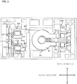
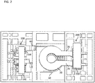
- an electronic device may have a primary coil 10, a secondary coil 20 disposed to face the primary coil 10, a coil sealing part 50 (see Fig. 3 ) sealing the primary coil 10 and the secondary coil 20 and being made of sealing resin, a primary-side electronic element 110 electrically connected to the primary coil 10, and a secondary-side electronic element 210 electrically connected to the secondary coil 20.
- the primary coil 10 may be constituted of a lead frame.
- a thickness of the secondary coil 20 may be greater than a thickness of the primary coil 10.
- the primary-side electronic element 110 may be provided on a primary-side extension part 60 that extends from the primary coil 10 to an outside of the coil sealing part 50.
- the secondary-side electronic element 210 may be provided on a secondary-side extension part 70 that extends from the secondary coil 20 to the outside of the coil sealing part 50.
- the primary-side electronic element 110 may be sealed with a primary-side sealing part 150.
- the primary-side sealing part 150 may be constituted of primary-side sealing resin.
- the secondary-side electronic element 210 may be sealed with a secondary-side sealing part 250.
- the secondary-side sealing part 250 may be constituted of secondary-side sealing resin.
- the primary-side sealing resin and the secondary-side sealing resin may be constituted of the same resin material, or may be constituted of resin materials that are different from each other.
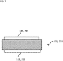
- a primary-side first electrode (for example, a source electrode) 111 and a primary-side second electrode (for example, a gate electrode) 112 may be provided on one surface of the primary-side electronic element 110, and a primary-side third electrode (for example, a drain electrode) 113 may be provided on another surface of the primary-side electronic element 110.
- the primary-side first electrode 111 and the primary-side conductor layer 130 may be connected via a primary-side first connector 116 (see Fig. 1 ) and a conductive adhesive (not illustrated) such as solder.
- the primary-side second electrode 112 and the primary-side conductor layer 130 may be connected via a primary-side second connector 117 (see Fig.
- the primary-side first electrode 111 may be provided on one surface of the primary-side electronic element 110, and the primary-side second electrode 112 may be provided on another surface of the primary-side electronic element 110.
- a secondary-side first electrode 211 may be provided on one surface of the secondary-side electronic element 210, and a secondary-side second electrode 212 may be provided on another surface of the secondary-side electronic element 210.
- the secondary-side first electrode 211 and the secondary-side conductor layer 230 may be connected via a secondary-side first connector and a conductive adhesive such as solder. Furthermore, as illustrated in Fig.
- the secondary-side first electrode (for example, a source electrode) 211 and the secondary-side second electrode (for example, a gate electrode) 212 may be provided on one surface of the secondary-side electronic element 210, and a secondary-side third electrode (for example, a drain electrode) 213 may be provided on another surface of the secondary-side electronic element 210.
- the secondary-side third electrode 213 and the secondary-side conductor layer 230 may be connected via a conductive adhesive such as solder.
- a first electronic module 100 may have a primary-side substrate 120, a plurality of primary-side conductor layers 130 that is provided on one surface of the primary-side substrate 120, and a primary-side electronic element 110 that is provided on one surface of the primary-side conductor layer 130.
- the primary-side electronic element 110, a surface on one side of the primary-side substrate 120, and a surface on the one side of the primary-side conductor layer 130 may be sealed with the primary-side sealing part 150 (see Fig. 3 ).
- a second electronic module 200 may have a secondary-side substrate 220, a plurality of secondary-side conductor layers 230 that is provided on one surface of the secondary-side substrate 220, and a secondary-side electronic element 210 that is provided on one surface of the secondary-side conductor layer 230.
- the secondary-side electronic element 210, a surface on the one side of the secondary-side substrate 220, and a surface on the one side of the secondary-side conductor layer 230 may be sealed with the secondary-side sealing part 250.
- the primary-side electronic element 110 may be provided on each of the one side and another side of the primary-side extension part 60.
- a primary-side first electrode (for example, a source electrode) 111 of a primary-side electronic element 110 that is located on the other side of the primary-side extension part 60 and a primary-side third electrode (for example, a drain electrode) 113 of a primary-side electronic element 110 that is located on the one side of the primary-side extension part 60 may be electrically connected by the primary-side extension part 60.
- a primary-side connecting body 190 that connects a plurality of primary-side electronic elements 110 that is provided on the one side of the primary-side extension part 60 may be provided.
- primary-side first electrodes (for example, source electrodes) 111 of a plurality of primary-side electronic elements 110 that is located on the one side of the primary-side extension part 60 may be electrically connected by the primary-side connecting body 190.
- a plurality of primary-side electronic elements 110 may be provided, and from among the plurality of primary-side electronic elements 110, one primary-side electronic element 110 or two or more primary-side electronic elements 110 may be provided on the primary-side extension part 60 via a conductive adhesive such as solder, and the remaining primary-side electronic elements 110 may be provided on the primary-side substrate 120 via a conductive adhesive such as solder.
- a primary-side electronic element 110 on a leftmost side and a primary-side electronic element 110 on a rightmost side are provided on the primary-side extension part 60, and two primary-side electronic elements 110 in the middle are provided on primary-side conductor layers 130 that are provided on the primary-side substrate 120.
- the secondary-side electronic element 210 may be provided on each of the one side and the other side of the secondary-side extension part 70.
- a secondary-side first electrode (for example, a source electrode) 211 of a secondary-side electronic element 210 that is located on the other side of the secondary-side extension part 70 and a secondary-side third electrode (for example, a drain electrode) 213 of a secondary-side electronic element 210 that is located on the one side of the secondary-side extension part 70 may be electrically connected by the secondary-side extension part 70.
- a protrusion part 71 may be provided on the other side of the secondary-side extension part 70, and the protrusion part 71 may be connected to an electrode 211 or 212 of the secondary-side electronic element 210.
- the primary-side extension part 60 may also have a protrusion part 61. Then, this protrusion part 61 may be connected to an electrode 111 or 112 of the primary-side electronic element 110.
- a secondary-side connecting body 290 that connects a plurality of secondary-side electronic elements 210 that is provided on the one side of the secondary-side extension part 70 may be provided.
- secondary-side first electrodes for example, source electrodes
- a protrusion part 291 may be provided on the other side of the secondary-side connecting body 290, and the protrusion part 291 may be connected to the electrode 211 or 212 of the secondary-side electronic element 210.
- a protrusion part 191 may be provided on the other side of the primary-side connecting body 190, and the protrusion part 191 may be connected to the electrode 111 or 112 of the primary-side electronic element 110.
- a plurality of secondary-side electronic elements 210 may be provided, and from among the plurality of secondary-side electronic elements 210, one secondary-side electronic element 210 or two or more secondary-side electronic elements 210 may be provided on the secondary-side extension part 70, and the remaining secondary-side electronic elements 210 may be provided on the secondary-side substrate 220.
- two secondary-side electronic elements 210 are provided on the secondary-side extension part 70, and two secondary-side electronic elements 210 are provided on secondary-side conductor layers 230 that are provided on the secondary-side substrate 220.
- the primary coil 10 may have a first coil 10a and a second coil 10b coupled to the first coil 10a.
- the second coil 10b may be provided on the one side of the first coil 10a, and the first coil 10a and the second coil 10b may be coupled by a connecting part 19 that extends along a first direction and has a linear shape.
- the connecting part 19 does not need to be completely parallel to the first direction, and may be inclined with respect to the first direction.
- An aspect of "extending along the first direction” also includes an aspect of extending to be inclined with respect to the first direction, as described above.
- the secondary coil 20 may be provided on the one side of the second coil 10b.
- the first coil 10a and the second coil 10b of the primary coil 10 may have the same number of turns, or may have numbers of turns that are different from each other.
- each of the numbers of turns of the first coil 10a and the second coil 10b of the primary coil 10 may be 5.
- the number of turns of the secondary coil 20 may be 1, or may be 2 or more.
- the number of turns of the secondary coil 20 may be less than 1, and the secondary coil 20 may have an aspect of not being wound one turn.
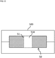
- a core 500 that passes through the primary coil 10 and the secondary coil 20 may be provided.
- the core 500 may have a leg part 510, and the leg part 510 may be provided to pass through an opening part 51 that is provided in the coil sealing part 50.
- the leg part 510 of the core 500 may be provided to abut onto an inner peripheral surface of the coil sealing part 50.
- An outer peripheral part of the core 500 may be provided to cover an outer periphery of the coil sealing part 50.
- the primary-side extension part 60 may have a primary-side first extension part 60a, and a primary-side second extension part 60b that is located on the one side relative to the primary-side first extension part 60a.
- the first coil 10a of the primary coil 10 and the primary-side first extension part 60a are constituted of a lead frame, and a member in which the first coil 10a and the primary-side first extension part 60a are integrated can be formed by removing an outer frame of the lead frame.
- the second coil 10b of the primary coil 10 and the primary-side second extension part 60b that is provided on the one side relative to the primary-side first extension part 60a may be constituted of a lead frame. In this case, by removing an outer frame of the lead frame, a member in which the second coil 10b and the primary-side second extension part 60b are integrated can be formed.
- a member in which a next coil and the secondary-side extension part 70 are integrated can be easily manufactured, by forming the secondary coil 20 and the secondary-side extension part 70 in a member such as a lead frame and removing an unnecessary portion.
- a cooling body 350 such as a heat sink may be provided on another surface (a back surface) of the coil sealing part 50, another surface (a back surface) of the primary-side sealing part 150, and another surface (a back surface) of the secondary-side sealing part 250.
- a cooling body 350 such as a heat sink may be provided on another surface (a back surface) of the coil sealing part 50, another surface (a back surface) of the primary-side sealing part 150, and another surface (a back surface) of the secondary-side sealing part 250.
- the primary-side electronic element 110 has a primary-side first electronic element 110a, a primary-side connecting body 115 that is provided on the primary-side first electronic element 110a, and a primary-side second electronic element 110b that is provided on the primary-side connecting body 115 is employed.
- the other configuration is similar to a configuration in the first embodiment, and all of the aspects described in the first embodiment can be employed.
- the members described in the first embodiment are described by using the same reference signs.
- the primary-side first electronic element 110a of the primary-side electronic element 110 may be provided on the primary-side extension part 60 via a conductive adhesive such as solder.
- the conductive adhesive such as solder may also be provided between the primary-side first electronic element 110a and the primary-side connecting body 115 and between the primary-side connecting body 115 and the primary-side second electronic element 110b.
- the primary-side electronic element 110 may only be provided on the one side of the primary-side extension part 60 (See a primary-side electronic element 110 on a rightmost side in Fig. 8 .
- This primary-side electronic element 110 changes to an aspect having the primary-side first electronic element 110a, the primary-side connecting body 115, and the primary-side second electronic element 110b.).
- the primary-side electronic element 110 may only be provided on the other side of the primary-side extension part 60.
- the primary-side electronic element 110 may be provided on both the one side and the other side of the primary-side extension part 60 (See two primary-side electronic elements 110 on a left-hand side in Fig. 8 . Each of these two primary-side electronic elements 110 changes to an aspect having the primary-side first electronic element 110a, the primary-side connecting body 115, and the primary-side second electronic element 110b.).
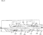
- the secondary-side electronic element 210 has a secondary-side first electronic element 210a, a secondary-side connecting body 215 that is provided on the secondary-side first electronic element 210a, and a secondary-side second electronic element 210b that is provided on the secondary-side connecting body 215 is employed.
- the other configuration is similar to a configuration in the first embodiment or the second embodiment, and all of the aspects described in each of the embodiments described above can be employed.
- the members described in each of the embodiments described above are described by using the same reference signs.
- the secondary-side first electronic element 210a of the secondary-side electronic element 210 may be provided on the secondary-side extension part 70 via a conductive adhesive such as solder.
- the conductive adhesive such as solder may also be provided between the secondary-side first electronic element 210a and the secondary-side connecting body 215 and between the secondary-side connecting body 215 and the secondary-side second electronic element 210b.
- the secondary-side electronic element 210 may only be provided on the one side of the secondary-side extension part 70.
- the secondary-side electronic element 210 may only be provided on the other side of the secondary-side extension part 70.
- the primary-side electronic element 110 may be provided on both the one side and the other side of the primary-side extension part 60 (See two secondary-side electronic elements 210 on a left-hand or right-hand side in Fig. 9 . Each of these two secondary-side electronic elements 110 changes to an aspect having the secondary-side first electronic element 210a, the secondary-side connecting body 215, and the secondary-side second electronic element 210b.) .
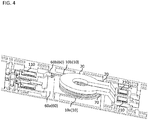
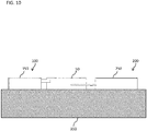
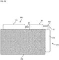
- a first bent part 310 is provided in the primary-side extension part 60 between the coil sealing part 50 and the primary-side sealing part 150 .
- the other configuration is similar to a configuration in the first embodiment to the third embodiment, and all of the aspects described in each of embodiments can be employed.
- the members described in each of embodiments are described by using the same reference signs.
- the coil sealing part 50 and the secondary-side sealing part 250 can be disposed along a plane direction, and the primary-side sealing part 150 can be disposed along a direction that is bent by a predetermined angle (for example, 60 degrees, 90 degrees, 120 degrees, or the like) with respect to the plane direction. Therefore, a size in a certain plane direction can be reduced.
- a predetermined angle for example, 60 degrees, 90 degrees, 120 degrees, or the like
- such bending enables a reduction in an influence of noise or the like generated in the primary-side electronic element 110 sealed with the primary-side sealing part 150 on the secondary-side electronic element 210 sealed with the secondary-side sealing part 250, and also enables a reduction in an influence of noise or the like generated in the secondary-side electronic element 210 on the secondary-side electronic element 210 sealed with the primary-side sealing part 150.
- the cooling body 350 such as a heat sink may be provided on the back surface of the coil sealing part 50, the back surface of the primary-side sealing part 150, and the back surface of the secondary-side sealing part 250.
- the cooling body 350 such as a heat sink may be provided on the back surface of the coil sealing part 50, the back surface of the primary-side sealing part 150, and the back surface of the secondary-side sealing part 250.
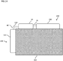
- a second bent part 320 is provided in the secondary-side extension part 70 between the coil sealing part 50 and the secondary-side sealing part 250 .
- the other configuration is similar to a configuration in the first embodiment to the third embodiment, and all of the aspects described in each of the embodiments can be employed.
- the members described in each of the embodiments are described by using the same reference signs.
- the coil sealing part 50 and the primary-side sealing part 150 can be disposed along a plane direction, and the secondary-side sealing part 250 can be disposed along a direction that is bent by a predetermined angle (for example, 60 degrees, 90 degrees, 120 degrees, or the like) with respect to the plane direction. Therefore, a size in a certain plane direction can be reduced.
- a predetermined angle for example, 60 degrees, 90 degrees, 120 degrees, or the like
- such bending enables a reduction in an influence of noise or the like generated in the primary-side electronic element 110 sealed with the primary-side sealing part 150 on the secondary-side electronic element 210 sealed with the secondary-side sealing part 250, and also enables a reduction in an influence of noise or the like generated in the secondary-side electronic element 210 on the secondary-side electronic element 210 sealed with the primary-side sealing part 150.
- the cooling body 350 such as a heat sink may be provided on the back surface of the coil sealing part 50, the back surface of the primary-side sealing part 150, and the back surface of the secondary-side sealing part 250.
- the cooling body 350 such as a heat sink may be provided on the back surface of the coil sealing part 50, the back surface of the primary-side sealing part 150, and the back surface of the secondary-side sealing part 250.
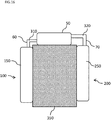
- the first bent part 310 is provided in the primary-side extension part 60 between the coil sealing part 50 and the primary-side sealing part 150 and the second bent part 320 is provided in the secondary-side extension part 70 between the coil sealing part 50 and the secondary-side sealing part 250 is employed.
- the other configuration is similar to a configuration in the first embodiment to the third embodiment, and all of the aspects described in each of embodiments can be employed.
- the members described in each of embodiments are described by using the same reference signs.
- the coil sealing part 50, the primary-side sealing part 150, and the secondary-side sealing part 250 can be respectively disposed along plane directions that are different from each other. Furthermore, the primary-side sealing part 150 and the secondary-side sealing part 250 can also be disposed in such a way that respective back surfaces face each other.
- the coil sealing part 50 and the primary-side sealing part 150 may be disposed to be bent by a first angle (for example, 60 degrees, 90 degrees, 120 degrees, or the like) with respect to each other, and the coil sealing part 50 and the secondary-side sealing part 250 may be disposed to be bent by a second angle (for example, 60 degrees, 90 degrees, 120 degrees, or the like) with respect to each other.
- the cooling body 350 such as a heat sink may be provided on the back surface of the coil sealing part 50, the back surface of the primary-side sealing part 150, and the back surface of the secondary-side sealing part 250.
- the cooling body 350 such as a heat sink may be provided on the back surface of the coil sealing part 50, the back surface of the primary-side sealing part 150, and the back surface of the secondary-side sealing part 250.
- disposition can be performed in such a way that the back surface of the coil sealing part 50, the back surface of the primary-side sealing part 150, and the back surface of the secondary-side sealing part 250 respectively abut onto three surfaces of the cooling body 350 that is made of a heat sink or the like, and there is an advantage in which a high cooling effect can be expected.
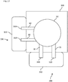
- the primary-side terminal 60 and the secondary-side terminal 70 do not need to be provided linearly.
- the primary-side terminal 60 and the secondary-side terminal 70 may be provided to be orthogonal to each other in a plane direction, or may be provided to cross each other at an angle that is different from 90 degrees in the plane direction.
- Fig. 17 illustrates an aspect in which the primary-side terminal 60 and the secondary-side terminal 70 are orthogonal to each other in the plane direction.
- the primary-side sealing part 150 and the secondary-side sealing part 250 can be disposed in any direction of the plane direction, and can be bent by using the first bent part 310 and the second bent part 320.
Landscapes
- Engineering & Computer Science (AREA)
- Power Engineering (AREA)
- Dc-Dc Converters (AREA)
- Coils Or Transformers For Communication (AREA)
- Coils Of Transformers For General Uses (AREA)
Applications Claiming Priority (1)
| Application Number | Priority Date | Filing Date | Title |
|---|---|---|---|
| PCT/JP2018/024765 WO2020003482A1 (ja) | 2018-06-29 | 2018-06-29 | 電子装置 |
Publications (2)
| Publication Number | Publication Date |
|---|---|
| EP3817014A1 true EP3817014A1 (de) | 2021-05-05 |
| EP3817014A4 EP3817014A4 (de) | 2022-02-23 |
Family
ID=68986809
Family Applications (1)
| Application Number | Title | Priority Date | Filing Date |
|---|---|---|---|
| EP18924681.2A Pending EP3817014A4 (de) | 2018-06-29 | 2018-06-29 | Elektronische vorrichtung |
Country Status (5)
| Country | Link |
|---|---|
| US (1) | US12272489B2 (de) |
| EP (1) | EP3817014A4 (de) |
| JP (1) | JPWO2020003482A1 (de) |
| CN (1) | CN112352296B (de) |
| WO (1) | WO2020003482A1 (de) |
Families Citing this family (1)
| Publication number | Priority date | Publication date | Assignee | Title |
|---|---|---|---|---|
| JP7149330B2 (ja) * | 2018-06-29 | 2022-10-06 | 新電元工業株式会社 | 電子装置 |
Family Cites Families (28)
| Publication number | Priority date | Publication date | Assignee | Title |
|---|---|---|---|---|
| JPH05283247A (ja) | 1992-04-03 | 1993-10-29 | Sony Corp | トランス |
| US6181231B1 (en) * | 1998-04-06 | 2001-01-30 | Silicon Graphics, Inc. | Diamond-based transformers and power convertors |
| JP4218205B2 (ja) * | 2000-11-27 | 2009-02-04 | 株式会社デンソー | 二バッテリ搭載型車両用降圧型dc−dcコンバータ装置 |
| JP3792635B2 (ja) * | 2001-12-14 | 2006-07-05 | 富士通株式会社 | 電子装置 |
| JP4123768B2 (ja) * | 2001-12-18 | 2008-07-23 | 株式会社デンソー | 成形コイルを用いる車両用降圧トランス |
| TWI278876B (en) * | 2006-01-03 | 2007-04-11 | Delta Electronics Inc | Transformer structure |
| US7649434B2 (en) * | 2006-01-31 | 2010-01-19 | Virginia Tech Intellectual Properties, Inc. | Multiphase voltage regulator having coupled inductors with reduced winding resistance |
| US20090196973A1 (en) * | 2008-02-01 | 2009-08-06 | Rich Products Corporation | Foam Compositions |
| JP4862846B2 (ja) * | 2008-02-29 | 2012-01-25 | 株式会社デンソー | 電源トランス及びインダクタンス部品 |
| TWI324351B (en) * | 2008-06-13 | 2010-05-01 | Delta Electronics Inc | Transformer structure and rectifier circuit using the same |
| US8169050B2 (en) * | 2008-06-26 | 2012-05-01 | International Business Machines Corporation | BEOL wiring structures that include an on-chip inductor and an on-chip capacitor, and design structures for a radiofrequency integrated circuit |
| US7969002B2 (en) * | 2008-10-29 | 2011-06-28 | Maxim Integrated Products, Inc. | Integrated circuit packages incorporating an inductor and methods |
| JP2010123898A (ja) * | 2008-11-21 | 2010-06-03 | Toyota Motor Corp | 半導体装置 |
| US20100301987A1 (en) * | 2009-05-27 | 2010-12-02 | Stmicroelectronics S.A. | Millimeter wave transformer with a high transformation factor and a low insertion loss |
| US8237535B2 (en) * | 2010-04-16 | 2012-08-07 | World Properties, Inc. | Integral planar transformer and busbar |
| CN102971811B (zh) * | 2010-07-26 | 2016-04-13 | 三菱电机株式会社 | 变压器 |
| US9093434B2 (en) * | 2011-04-04 | 2015-07-28 | Rohm Co., Ltd. | Semiconductor device and method for manufacturing semiconductor device |
| JP2012231616A (ja) * | 2011-04-27 | 2012-11-22 | Diamond Electric Mfg Co Ltd | 車載用電力変換装置 |
| US8675368B2 (en) * | 2011-08-18 | 2014-03-18 | Taiwan Semiconductor Manufacturing Company, Ltd. | Vertically oriented semiconductor device and shielding structure thereof |
| JP5998774B2 (ja) | 2012-09-11 | 2016-09-28 | Tdk株式会社 | プリントコイル型トランスおよび電源装置 |
| CN103366935A (zh) * | 2013-07-30 | 2013-10-23 | 华为技术有限公司 | 平板变压器结构 |
| JP6317948B2 (ja) * | 2014-02-24 | 2018-04-25 | 新電元工業株式会社 | トランスのコイル接続構造、及び、トランス |
| EP2924451B1 (de) * | 2014-03-24 | 2019-01-09 | LEM Intellectual Property SA | Stromwandler |
| DE102015213648A1 (de) | 2015-07-20 | 2017-01-26 | Lenze Automation Gmbh | Verfahren zum Betreiben eines Frequenzumrichters und Frequenzumrichter |
| JP6552327B2 (ja) * | 2015-08-10 | 2019-07-31 | ダイヤモンド電機株式会社 | 電力変換装置 |
| JP6551546B2 (ja) * | 2016-01-27 | 2019-07-31 | 株式会社村田製作所 | インダクタ部品およびその製造方法 |
| JP6624160B2 (ja) * | 2017-05-23 | 2019-12-25 | オムロン株式会社 | トランス一体型プリント基板 |
| US20200258675A1 (en) * | 2019-02-08 | 2020-08-13 | Lear Corporation | Hybrid transformer for dc/dc converter |
-
2018
- 2018-06-29 WO PCT/JP2018/024765 patent/WO2020003482A1/ja not_active Ceased
- 2018-06-29 JP JP2020526843A patent/JPWO2020003482A1/ja active Pending
- 2018-06-29 EP EP18924681.2A patent/EP3817014A4/de active Pending
- 2018-06-29 US US17/255,954 patent/US12272489B2/en active Active
- 2018-06-29 CN CN201880094951.6A patent/CN112352296B/zh active Active
Also Published As
| Publication number | Publication date |
|---|---|
| JPWO2020003482A1 (ja) | 2021-08-12 |
| US12272489B2 (en) | 2025-04-08 |
| CN112352296B (zh) | 2024-05-28 |
| CN112352296A (zh) | 2021-02-09 |
| EP3817014A4 (de) | 2022-02-23 |
| US20210272748A1 (en) | 2021-09-02 |
| WO2020003482A1 (ja) | 2020-01-02 |
Similar Documents
| Publication | Publication Date | Title |
|---|---|---|
| US10559553B2 (en) | Power module | |
| US9795049B2 (en) | Semiconductor device | |
| US11646273B2 (en) | Module | |
| KR101823805B1 (ko) | 전력 반도체 장치 | |
| US12051536B2 (en) | Electronic device | |
| EP3817014A1 (de) | Elektronische vorrichtung | |
| EP3817017A1 (de) | Magnetische komponente | |
| US9520793B2 (en) | Stacked power converter assembly | |
| US11967451B2 (en) | Electronic device | |
| US12580123B2 (en) | Isolator | |
| JP2025110920A (ja) | 電力用半導体装置 | |
| WO2024181376A1 (ja) | パワー半導体モジュール及び電力変換装置 |
Legal Events
| Date | Code | Title | Description |
|---|---|---|---|
| STAA | Information on the status of an ep patent application or granted ep patent |
Free format text: STATUS: THE INTERNATIONAL PUBLICATION HAS BEEN MADE |
|
| PUAI | Public reference made under article 153(3) epc to a published international application that has entered the european phase |
Free format text: ORIGINAL CODE: 0009012 |
|
| STAA | Information on the status of an ep patent application or granted ep patent |
Free format text: STATUS: REQUEST FOR EXAMINATION WAS MADE |
|
| 17P | Request for examination filed |
Effective date: 20210126 |
|
| AK | Designated contracting states |
Kind code of ref document: A1 Designated state(s): AL AT BE BG CH CY CZ DE DK EE ES FI FR GB GR HR HU IE IS IT LI LT LU LV MC MK MT NL NO PL PT RO RS SE SI SK SM TR |
|
| DAV | Request for validation of the european patent (deleted) | ||
| DAX | Request for extension of the european patent (deleted) | ||
| A4 | Supplementary search report drawn up and despatched |
Effective date: 20220124 |
|
| RIC1 | Information provided on ipc code assigned before grant |
Ipc: H02M 3/28 20060101ALI20220118BHEP Ipc: H01F 27/32 20060101ALI20220118BHEP Ipc: H01F 27/28 20060101AFI20220118BHEP |
|
| STAA | Information on the status of an ep patent application or granted ep patent |
Free format text: STATUS: EXAMINATION IS IN PROGRESS |
|
| 17Q | First examination report despatched |
Effective date: 20240521 |