EP3817057A1 - Vorrichtung mit pixelinsel, herstellungsverfahren dafür und anzeigevorrichtung - Google Patents
Vorrichtung mit pixelinsel, herstellungsverfahren dafür und anzeigevorrichtung Download PDFInfo
- Publication number
- EP3817057A1 EP3817057A1 EP19783406.2A EP19783406A EP3817057A1 EP 3817057 A1 EP3817057 A1 EP 3817057A1 EP 19783406 A EP19783406 A EP 19783406A EP 3817057 A1 EP3817057 A1 EP 3817057A1
- Authority
- EP
- European Patent Office
- Prior art keywords
- inter
- island
- islands
- connection line
- trench
- Prior art date
- Legal status (The legal status is an assumption and is not a legal conclusion. Google has not performed a legal analysis and makes no representation as to the accuracy of the status listed.)
- Pending
Links
Images


Classifications
-
- H—ELECTRICITY
- H10—SEMICONDUCTOR DEVICES; ELECTRIC SOLID-STATE DEVICES NOT OTHERWISE PROVIDED FOR
- H10K—ORGANIC ELECTRIC SOLID-STATE DEVICES
- H10K59/00—Integrated devices, or assemblies of multiple devices, comprising at least one organic light-emitting element covered by group H10K50/00
- H10K59/10—OLED displays
- H10K59/12—Active-matrix OLED [AMOLED] displays
-
- H—ELECTRICITY
- H10—SEMICONDUCTOR DEVICES; ELECTRIC SOLID-STATE DEVICES NOT OTHERWISE PROVIDED FOR
- H10D—INORGANIC ELECTRIC SEMICONDUCTOR DEVICES
- H10D86/00—Integrated devices formed in or on insulating or conducting substrates, e.g. formed in silicon-on-insulator [SOI] substrates or on stainless steel or glass substrates
- H10D86/01—Manufacture or treatment
- H10D86/021—Manufacture or treatment of multiple TFTs
-
- H—ELECTRICITY
- H10—SEMICONDUCTOR DEVICES; ELECTRIC SOLID-STATE DEVICES NOT OTHERWISE PROVIDED FOR
- H10D—INORGANIC ELECTRIC SEMICONDUCTOR DEVICES
- H10D86/00—Integrated devices formed in or on insulating or conducting substrates, e.g. formed in silicon-on-insulator [SOI] substrates or on stainless steel or glass substrates
- H10D86/40—Integrated devices formed in or on insulating or conducting substrates, e.g. formed in silicon-on-insulator [SOI] substrates or on stainless steel or glass substrates characterised by multiple TFTs
- H10D86/411—Integrated devices formed in or on insulating or conducting substrates, e.g. formed in silicon-on-insulator [SOI] substrates or on stainless steel or glass substrates characterised by multiple TFTs characterised by materials, geometry or structure of the substrates
-
- H—ELECTRICITY
- H10—SEMICONDUCTOR DEVICES; ELECTRIC SOLID-STATE DEVICES NOT OTHERWISE PROVIDED FOR
- H10D—INORGANIC ELECTRIC SEMICONDUCTOR DEVICES
- H10D86/00—Integrated devices formed in or on insulating or conducting substrates, e.g. formed in silicon-on-insulator [SOI] substrates or on stainless steel or glass substrates
- H10D86/40—Integrated devices formed in or on insulating or conducting substrates, e.g. formed in silicon-on-insulator [SOI] substrates or on stainless steel or glass substrates characterised by multiple TFTs
- H10D86/441—Interconnections, e.g. scanning lines
-
- H—ELECTRICITY
- H10—SEMICONDUCTOR DEVICES; ELECTRIC SOLID-STATE DEVICES NOT OTHERWISE PROVIDED FOR
- H10D—INORGANIC ELECTRIC SEMICONDUCTOR DEVICES
- H10D86/00—Integrated devices formed in or on insulating or conducting substrates, e.g. formed in silicon-on-insulator [SOI] substrates or on stainless steel or glass substrates
- H10D86/40—Integrated devices formed in or on insulating or conducting substrates, e.g. formed in silicon-on-insulator [SOI] substrates or on stainless steel or glass substrates characterised by multiple TFTs
- H10D86/60—Integrated devices formed in or on insulating or conducting substrates, e.g. formed in silicon-on-insulator [SOI] substrates or on stainless steel or glass substrates characterised by multiple TFTs wherein the TFTs are in active matrices
-
- H—ELECTRICITY
- H10—SEMICONDUCTOR DEVICES; ELECTRIC SOLID-STATE DEVICES NOT OTHERWISE PROVIDED FOR
- H10K—ORGANIC ELECTRIC SOLID-STATE DEVICES
- H10K59/00—Integrated devices, or assemblies of multiple devices, comprising at least one organic light-emitting element covered by group H10K50/00
- H10K59/10—OLED displays
- H10K59/12—Active-matrix OLED [AMOLED] displays
- H10K59/1201—Manufacture or treatment
-
- H—ELECTRICITY
- H10—SEMICONDUCTOR DEVICES; ELECTRIC SOLID-STATE DEVICES NOT OTHERWISE PROVIDED FOR
- H10K—ORGANIC ELECTRIC SOLID-STATE DEVICES
- H10K59/00—Integrated devices, or assemblies of multiple devices, comprising at least one organic light-emitting element covered by group H10K50/00
- H10K59/10—OLED displays
- H10K59/12—Active-matrix OLED [AMOLED] displays
- H10K59/131—Interconnections, e.g. wiring lines or terminals
-
- H—ELECTRICITY
- H10—SEMICONDUCTOR DEVICES; ELECTRIC SOLID-STATE DEVICES NOT OTHERWISE PROVIDED FOR
- H10F—INORGANIC SEMICONDUCTOR DEVICES SENSITIVE TO INFRARED RADIATION, LIGHT, ELECTROMAGNETIC RADIATION OF SHORTER WAVELENGTH OR CORPUSCULAR RADIATION
- H10F39/00—Integrated devices, or assemblies of multiple devices, comprising at least one element covered by group H10F30/00, e.g. radiation detectors comprising photodiode arrays
- H10F39/80—Constructional details of image sensors
- H10F39/802—Geometry or disposition of elements in pixels, e.g. address-lines or gate electrodes
-
- H—ELECTRICITY
- H10—SEMICONDUCTOR DEVICES; ELECTRIC SOLID-STATE DEVICES NOT OTHERWISE PROVIDED FOR
- H10F—INORGANIC SEMICONDUCTOR DEVICES SENSITIVE TO INFRARED RADIATION, LIGHT, ELECTROMAGNETIC RADIATION OF SHORTER WAVELENGTH OR CORPUSCULAR RADIATION
- H10F39/00—Integrated devices, or assemblies of multiple devices, comprising at least one element covered by group H10F30/00, e.g. radiation detectors comprising photodiode arrays
- H10F39/80—Constructional details of image sensors
- H10F39/803—Pixels having integrated switching, control, storage or amplification elements
-
- H—ELECTRICITY
- H10—SEMICONDUCTOR DEVICES; ELECTRIC SOLID-STATE DEVICES NOT OTHERWISE PROVIDED FOR
- H10K—ORGANIC ELECTRIC SOLID-STATE DEVICES
- H10K2102/00—Constructional details relating to the organic devices covered by this subclass
- H10K2102/301—Details of OLEDs
- H10K2102/311—Flexible OLED
Definitions
- the present disclosure relates to the field of display technologies, and in particular, to a device having a pixel island, a method for preparing the same, and a display device.
- OLED Organic Light Emitting Diode
- OLED display substrates One of the advantages of OLED display substrates is flexibility, and with the OLED display substrates in which OLED devices are formed on a flexible substrate, flexible display devices can be achieved.
- wearable devices it has placed higher demands on the tensile properties of OLED flexible panels. Since each pixel of the OLED display substrate is provided with a separate driving circuit, this results in not only a higher pixel density but also dense wirings. Therefore, it is relatively difficult to realize stretchable OLED display substrate. In addition, the bending property of the OLED display substrate may also be affected.
- One of the objects of some embodiments of the present disclosure is to provide a device, a method of preparing the same, and a display device.
- a device comprising: a flexible substrate; at least two islands on the flexible substrate, each of the islands including a semiconductor layer, adjacent islands being separated by a trench; at least one inter-island connection line each for electrically connecting corresponding islands.
- the device further comprises: an organic insulating material filled in the trench.
- the at least one inter-island connection line is configured to: span over a corresponding trench, or be at least partially received in the corresponding trench.
- the inter-island connection line is made of a flexible material or has a shape suitable for being stretched.
- the islands have a shape comprising circle or polygon, and the polygon comprises any one of a triangle, a diamond, and a rectangle.
- the islands are adaptable to form pixels therein, the pixel comprising a device for receiving or emitting light and a semiconductor device associated therewith.
- the device further comprises: an insulating layer located between the at least one inter-island connection line and corresponding islands, wherein the at least one inter-island connection line is electrically connected to a component in the corresponding island through a hole in the insulating layer.
- the insulating layer comprises one of the following: an organic insulating layer or an inorganic insulating layer.
- the islands include thin film transistors which include sources and drains, and wherein the inter-island connection line is located at a different layer from the sources and the drains.
- the device is a display substrate or a sensor substrate.
- each of the islands includes: a buffer layer over the flexible substrate; and the semiconductor layer over the buffer layer, wherein the trench extends to the flexible substrate.
- each of the islands comprises a component for electrical connection, wherein each of the at least one inter-island connection line is electrically connected to the component for electrical connection of the corresponding island, wherein the inter-island connection line is located at a different layer from the component for electrical connection.
- a display device comprising a device according to any embodiments.
- a method of preparing a device comprising: forming at least two islands on the flexible substrate, the adjacent islands being separated by a trench, the island comprising a semiconductor layer; forming at least one inter-island connection line for electrically connecting corresponding islands.
- the at least one inter-island connection line is configured to be stretchable.
- the at least inter-island connection line spans over the corresponding trench or is received in the corresponding trench.
- the method further comprises, after forming the at least two islands and prior to forming the at least one inter-island connection line: filling the trench with an insulating material.
- the insulating material comprises an organic insulating material.
- the method further comprises, after filling the trench with the insulating material and prior to forming the at least one inter-island connection line: forming an insulating layer over the islands and the insulating material, the insulating layer including at least one opening; wherein, forming the at least one inter-island connection line comprises: forming the at least one inter-island connection line over the insulating layer, the at least one inter-island connection line filling a corresponding opening and being electrically connected with a corresponding island.
- each of the islands comprises a component for electrical connection, wherein each of the at least one inter-island connection line is electrically connected to the component for electrical connection of a corresponding island, wherein the inter-island connection line is located at a different layer from the component for electrical connection.
- a pixel region are divided into a plurality of pixel islands by trenches, and signal connection between adjacent pixel islands are achieved by providing inter-island connection lines over the corresponding trenches.
- the tensile properties and the bending properties of the display substrates can be effectively improved while ensuring signal communication.
- display substrates or sensor substrates having improved tensile properties and bending properties such as a bendable OLED display substrate, a CIMS sensor substrate, or the like, can be provided.
- a device which may comprises: a flexible substrate; at least two islands on the flexible substrate, wherein adjacent islands are separated by a trench; and at least one inter-island connection line each for connecting the corresponding islands.
- the island may comprise a semiconductor layer.
- the at least one inter-island connection line can be configured to be stretchable.
- display substrate As an example, and the island will be referred to as a pixel island.
- the device described in the present disclosure shall not be limited to the display substrate; for example, it may be a sensor substrate.
- the display substrate described herein can be applied to, but not limited to, a bendable OLED display.
- the device e.g., a display substrate
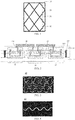
- the device may include a flexible substrate 10, a plurality of pixel islands 20 on the flexible substrate 10, trenches 30 between adjacent pixel islands 20, and inter-island connection lines 40 for connecting adjacent pixel islands 20.
- Fig. 2 schematically shows a partial cross-sectional view of the device shown in Fig. 1 .
- the pixel island is adaptable to form a pixel therein.
- the pixel may include a device for receiving or emitting light (e.g., a light emitting diode or photodiode, etc.) and a semiconductor device (such as, but not limited to, a switching device, a capacitor, etc.) associated with the device for receiving or emitting light.
- the pixels can be configured to receive or emit light.
- a pixel may include one or more sub-pixels, such as a sub-pixel for red, a sub-pixel for blue, a sub-pixel for green, and the like.
- the pixel or sub-pixel may include, for example, a light emitting diode.
- the pixel or sub-pixel may comprise, for example, a photodiode. It should be understood that the present disclosure is not limited to these cases.
- the pixel island 20 may be provided with a thin film transistor 200.
- the pixel island 20 may also be provided with components for electrical connection, for example, components electrically connected to the thin film transistor 200 or other electronic devices, such as but not limited to, terminals, doped active regions, metal wiring, or polysilicon wirings, etc..
- the components for electrical connection may be used for internal electrical connections.
- the components for electrical connection may also be used to carry signals or power, such as scan signals, data signals, and/or power supplies, etc. It is to be understood that the signal lines in an island can be connected in various manners known or future developed.
- the inter-island connection line 40 can be used to connect corresponding pixel islands.
- the inter-island connection line 40 electrically connects the electrical connection components (e.g., signal lines) of adjacent pixel islands 20 to achieve signal communication between adjacent pixel islands 20.
- the inter-island connection lines 40 may include, for example, a first inter-island connection line electrically connecting scan signal lines of adjacent pixel islands 20, and a second inter-island connection line electrically connecting data signal lines of adjacent pixel islands 20, and/or a third inter-island connection line electrically connecting the power lines of the adjacent pixel islands 20, and the like.
- a pixel island 20 may include at least one pixel unit. In some embodiments, a pixel island 20 can include a group of pixels. In some embodiments of the present disclosure, a pixel may include several sub-pixels, such as a sub-pixel for red, a sub-pixel for blue, a sub-pixel for green, and the like. Signal communication between respective groups of pixels (or sub-pixels) of adjacent pixel islands can be achieved by the inter-island connection lines 40.
- a pixel island 20 may include a plurality of pixels, and thin film transistors (e.g., control transistors) of the plurality of pixels are electrically connected to the scan signal lines. Since the adjacent pixel islands 20 are separated by a trench 300 disposed theirbetween, the scanning signal lines of the adjacent pixel islands 20 are independent from each other.
- the signal communication of the adjacent pixel islands 20 can be realized by providing the inter-island connection line 40 electrically connected to the two scanning signal lines of the adjacent pixel islands 20.
- the gate of the control transistor is electrically connected to the corresponding scanning signal line in the island, these two can be formed into an integral structure by a same patterning process in the preparation thereof. Therefore, in such a case, when the scanning signal lines in the adjacent pixel islands 20 are electrically connected through the inter-island connection line 40, it can be achieved by connecting the gates of the control transistors in the adjacent pixel islands 20 through the inter-island connection line 40.
- FIG. 2 illustrates an example in which each pixel island 20 includes one pixel (or sub-pixel), two or more pixels (or sub-pixels) may be included in each pixel island 20 in actual production; therefore, apparently the present disclosure shall not be limited to the illustrated embodiments.
- the electrical connection manner between the inter-island connection line 40 and other electrical connection components (for example, data signal lines or other signal lines) on the adjacent pixel islands 20 is similar to that for the above-mentioned scanning signal lines, and details are not repeatedly described herein.
- signal communications between adjacent pixel islands 20 can be achieved by providing trench(s) 30 to divide the pixel region into pixel islands 20 and providing an inter-island connection line 40 corresponding to the trench(s) 30.
- the tensile property and the bending property of the display substrate can be effectively improved, and signal communications can be ensured, thus, improved display substrate can be obtained.
- the inter-island connection line 40 can be received in or connected across and over the trench 30.
- the signal lines in the pixel islands 20 can be configured and routed in a normal manner.
- the signal line between adjacent pixel islands 20, that is, the inter-island connection line 40 may be partially disposed within the trench 30.
- the inter-island connection line 40 can be electrically isolated from the undesired components of the pixel islands to avoid undesired electrical connections.
- the inter-island connection line 40 can be provided to span across the trench 30 to effect signal line communication of adjacent two pixel islands 20.
- FIG. 2 is described by taking the inter-island connection line 40 connected over the trench 30 as an example, those skilled in the art would readily understand from the present disclosure that the inter-island connection line 40 can be configured in such a manner that it is at least partially accommodated in the trench 30, and thus this manner will not be description in further details.
- the trench 30 may be filled with an insulating material 300, such as, an organic insulating material.
- the signal loading mode is exemplified by taking the scanning signal as an example for the case where the foregoing display substrate is applied to an OLED display.
- the scan signals may be sequentially loaded to the scan signal lines corresponding to the pixels (or sub-pixels) of each row through cascaded GOA units.
- the same row of pixels within the pixel islands 20 are connected to the same intra-island scan signal line.
- the intra-island scanning signal lines of the adjacent two pixel islands 20 can be electrically connected through the inter-island connection lines 40 in a bridging manner to provide connection for scanning signal between the pixel islands 20.
- the scan signal can be transmitted from a pixel island 20 to another pixel island 20 through the inter-island connection line 40, and then transmitted from the another pixel island to a next pixel island in such a manner, till to all the target pixel islands.
- the scan signal loading for this stage is completed.
- the shape of the pixel island 20 may include any one of a circular shape or a polygon such as a triangle, a diamond, a rectangle, or the like; the present disclosure is not limited thereto.
- the inter-island connection line 40 a stretchable wire, such as a wire made of a flexible material and/or a wire suitable for stretching (e.g., the wire may have a curved shape), may be adopted.
- the inter-island connection line 40 may be a flexible wire, such as a wire formed of a flexible material such as silver nanowires, carbon nanotubes, or an organic conductive material.
- the flexible wire has good tensile property and can ensure an effective connection of the wires when the display substrate is bent.
- the inter-island connection line 40 may also adopt a curved wire or a polygonal-line wire, such as a horseshoe shape as shown in FIG. 3 , a wave shape as shown in FIG. 4 , or a zigzag shape as shown in FIG. 5 .
- the wire may be a metal wire. Since the stretchability of the metal wire is inferior to that of the flexible wire, if it is set to be a linear structure, the overall tensile property of the display substrate may be affected, so it is configured to have a curved structure or a polygonal-line structure, thereby tensile property of the metal wire can be improved, and effective connection of the wires can be ensured when the display substrate is bent.
- the polygonal line shape can be configured to have a certain curvature at the bends thereof.
- the inter-island connection line 40 may be a linear flexible wire, a curved/folded metal wire, or a curved/folded flexible wire.
- the inter-island connection line There is no particular limitation on the inter-island connection line as long as the inter-island connection line 40 has stretchability.
- the display substrate may further include a buffer layer 50 over the base substrate 10, and an insulating layer 60 located on a side of the inter-island connection line 40 near the base substrate 10.
- the insulating layer 60 may be located between the inter-island connection line and the corresponding islands.
- the inter-island connection line 40 can be electrically connected to the components in the corresponding islands, for example, through holes located in the insulating layer.
- the inter-island connection line 40 may be electrically connected to the gate of the thin film transistor 200 through the first hole 600 located in the insulating layer 60.
- the insulating layer 60 may be an organic insulating layer, and the trench 30 may penetrate the films/layers between the flexible substrate 10 and the insulating layer 60.
- the trench 30 can be configured to extend up to the flexible substrate 10. Since organic material has good tensile property, it is advantageous to configure the insulating layer 60 as an organic insulating layer to improve the tensile property of the display substrate.
- the insulating layer 60 may also be an inorganic insulating layer.
- the trench 30 may penetrate through the films/layers between the flexible substrate 10 and the inter-island connection line 40. Since the tensile property of inorganic material may be inferior to that of organic material, in this embodiment the trench 30 can be configured to also penetrate the inorganic insulating layer, which may be advantageous to improve the tensile property of the display substrate.
- the display substrate may further include an organic insulating material 300 filled in the trenches 30.
- the bottom of the organic insulating material 300 may be in contact with the flexible substrate 10, and the top of the organic insulating material 300 may contact or even penetrate the insulating layer 600. Since the organic insulating material 300 has good stretchability, it contributes to the overall tensile property of the display substrate.
- other materials in the trench 30 may be removed by, for example, an exposure and development step, leaving only the elastic organic insulating material 300 to form a deep trench in the trench 30 such that the inter-island connection line is remained in the deep trench in the trench 30.
- the thin film transistor 200 may include a semiconductor active layer 201 on a buffer layer 50, a gate insulating layer 202 over the semiconductor active layer 201, and a gate 203 over the gate insulating layer 202, an interlayer insulating layer 204 over the gate 203, and a source 207 and a drain 208.
- the source 207 and the drain 208 are electrically connected to the semiconductor active layer 201 through the second hole 205 and the third hole 206, respectively.
- the inter-island connection line 40 is located on a side of the interlayer insulating layer 204 facing away from the flexible substrate 10 and in a different layer from the source 207 and the drain 208.
- the pixel region can be divided into pixel islands 20. Wrings in the pixel island 20 can be normally routed. Between the pixel islands 20, an inter-island connection line 40 is provided after the source and drain metal layers are formed. According to the embodiments of the present disclosure, good stretchability can be obtained, and wiring layout can be facilitated.
- a method of preparing a device is also provided. As shown in FIG. 8 , the preparing method may include following steps.
- a plurality of pixel islands 20 and trenches 30 between adjacent pixel islands 20 are formed on a flexible substrate 10.
- the pixel islands 20 are provided with thin film transistors 200 and signal lines electrically connected to the thin film transistors 200.
- an inter-island connection line 40 for connecting adjacent pixel islands 20 is formed at a position corresponding to the trench 30.
- the inter-island connection line 40 electrically connects the signal lines of the adjacent pixel islands 20.
- the trenches 30 are provided to divide the pixel region into the pixel islands 20, and signal communication between adjacent pixel islands 20 is realized by the inter-island connection line 40. According to the embodiments of the present disclosure, the tensile property and the bending property of the display substrate can be effectively improved while ensuring signal communication, thus a bendable display substrate can be provided.
- a structure is formed on a flexible substrate 10.
- the structure may sequentially include a buffer layer 50, an optional light shielding layer (not shown) for thin film transistor 200, a semiconductor active layer 201, a gate insulating layer 202, a gate 203, and an interlayer insulating layer 204.
- the structure may further include electrical connection components, such as signal lines.
- the structure can be designed according to the distribution of the islands 20 predetermined in advance. In the area corresponding to the pixel islands 20 to be formed, the signal lines (if any) can be normally routed, and in a corresponding area where the trenches 30 among the pixel islands 20 are to be formed, the electrical connection components such as signal lines are not formed. That is, the electrical connection components are intra-island (or local) connection component.
- trenches 30 are formed in the structure.
- the trenches 30 penetrate through the interlayer insulating layer 204, the gate insulating layer 202, and the buffer layer 50 to separate the pixel islands 20.
- Holes 205 and 206 are formed in the interlayer insulating layer 204 and the gate insulating layer 202; the holes may be formed while forming the trenches 30, but the present disclosure is not limited thereto.
- Holes 205 and 206 can be used for the fabrication of source 207 and drain 208 of thin film transistor 200.
- the bottoms of the trenches 30 can also be configured to be proximate to the flexible substrate (i.e., only extend into the buffer substrate 50 (if any) and adjacent to the flexible substrate).
- the trenches 30 can be formed to extend to (or even into) the flexible substrate 10; as such, it is more advantageous to enhance the bending property of the display substrate.
- openings 205 and 206 are also possible to form openings 205 and 206 in the structure (or the corresponding island) while forming the trenches 30.
- the openings 205 and 206 can be used, for example, to form a source electrode and a drain electrode or contacts connected to the active layer; it should be understood that the present disclosure is not limited thereto.
- the trenches 30 are filled with an organic insulating material 300, such as, for example, polyimide (PI) or polydimethylsiloxane (PDMS) or the like.
- an organic insulating material 300 such as, for example, polyimide (PI) or polydimethylsiloxane (PDMS) or the like.
- PI polyimide
- PDMS polydimethylsiloxane
- the organic insulating material 300 preferably, a material which has good tensile property and can be processed by a photolithography and patterning process is adopted.
- a source 207 and a drain 208 are formed in the second hole 205 and the third hole 206, respectively.
- a basic structure of, for example, the transistor 200 in the pixel island 20 is formed.
- the trenches 30 may be formed first and filled with the organic insulating material 300; afterwards, the second hole 205 and the third hole 206 are formed and the source 207 and the drain 208 are therein; or vice versa.
- the second hole 205 and the third hole 206 may be formed first and the source 207 and the drain 208 may be formed therein, after which the trenches 30 are formed and filled with the organic insulating material 300.
- an insulating layer 60 (e.g., an organic insulating layer) is formed over the pixel islands 20. At least one opening (e.g., hole 600) may be formed in the insulating layer 60. Thereafter, an inter-island connection lines 40 are formed over the organic insulating layer 60. The inter-island connection lines 40 can be electrically connected to the thin film transistor 200 (for example, electrodes thereof) through the openings 600.
- the inter-island connection line 40 can include, for example but not be limited to, a first inter-island connection line electrically coupled to the scan signal line, a second inter-island connection line electrically coupled to the data signal line, and/or a third inter-island connection line electrically coupled to the power signal line, etc. Signal communication between adjacent pixel islands 20 can be achieved by the inter-island connection line(s) 40.
- a method of preparing a device is also provided. As shown in FIG. 12A , the method may include the following steps. In step S601, at least two islands are formed on a flexible substrate, and adjacent islands are separated by a trench, the island including a semiconductor layer. In step S607, at least one inter-island connection line is formed, and each inter-island connection line is used to electrically connect the corresponding islands. The at least one inter-island connection line is configured to be stretchable.
- the at least one inter-island connection line each is configured to span over a corresponding trench or received in a corresponding trench.
- a method of preparing a device is also provided. As shown in FIG. 12B , the method may include the following steps.
- step S601 at least two islands are formed on the flexible substrate, and adjacent islands are separated by a trench, the island including a semiconductor layer.
- step S603 the trench is filled with an insulating material.
- the insulating material may be, for example, an organic insulating material.
- step S605 an insulating layer is formed over the islands and the insulating material, the insulating layer including at least one opening.
- at least one inter-island connection line is formed over the insulating layer, and the at least one inter-island connection line fills a corresponding opening and is electrically connected to a corresponding island.
- each of the islands includes a component for electrical connection, wherein each of the at least one inter-island connection line is electrically coupled to a component for electrical connection of a corresponding island.
- the inter-island connection line may be in a different layer from the component for electrical connection.
- a display device comprising the above-described device (for example, a display substrate).
- the display device has good tensile property, and can be applied to a flexible display device, and particularly be suitable for a wearable device.
Landscapes
- Engineering & Computer Science (AREA)
- Microelectronics & Electronic Packaging (AREA)
- Manufacturing & Machinery (AREA)
- Devices For Indicating Variable Information By Combining Individual Elements (AREA)
- Electroluminescent Light Sources (AREA)
Applications Claiming Priority (2)
| Application Number | Priority Date | Filing Date | Title |
|---|---|---|---|
| CN201810671717.7A CN108878486A (zh) | 2018-06-26 | 2018-06-26 | 显示基板及其制备方法、显示装置 |
| PCT/CN2019/074412 WO2020001032A1 (zh) | 2018-06-26 | 2019-02-01 | 包括像素岛的装置及其制备方法以及显示装置 |
Publications (2)
| Publication Number | Publication Date |
|---|---|
| EP3817057A1 true EP3817057A1 (de) | 2021-05-05 |
| EP3817057A4 EP3817057A4 (de) | 2022-03-09 |
Family
ID=64295752
Family Applications (1)
| Application Number | Title | Priority Date | Filing Date |
|---|---|---|---|
| EP19783406.2A Pending EP3817057A4 (de) | 2018-06-26 | 2019-02-01 | Vorrichtung mit pixelinsel, herstellungsverfahren dafür und anzeigevorrichtung |
Country Status (5)
| Country | Link |
|---|---|
| US (1) | US11101296B2 (de) |
| EP (1) | EP3817057A4 (de) |
| JP (1) | JP7415245B2 (de) |
| CN (1) | CN108878486A (de) |
| WO (1) | WO2020001032A1 (de) |
Families Citing this family (29)
| Publication number | Priority date | Publication date | Assignee | Title |
|---|---|---|---|---|
| KR102462421B1 (ko) * | 2017-11-15 | 2022-11-03 | 삼성디스플레이 주식회사 | 디스플레이 장치 |
| CN108878486A (zh) * | 2018-06-26 | 2018-11-23 | 京东方科技集团股份有限公司 | 显示基板及其制备方法、显示装置 |
| CN109599402B (zh) * | 2018-12-03 | 2021-02-09 | 京东方科技集团股份有限公司 | 显示基板和显示装置 |
| CN111326067B (zh) * | 2018-12-13 | 2022-01-28 | 昆山工研院新型平板显示技术中心有限公司 | 显示面板及其制作方法和显示装置 |
| CN111326607B (zh) * | 2018-12-14 | 2021-05-25 | 昆山工研院新型平板显示技术中心有限公司 | 可拉伸显示面板及其制备方法、可拉伸显示装置 |
| CN109742119A (zh) * | 2019-01-08 | 2019-05-10 | 云谷(固安)科技有限公司 | 可拉伸显示器件及其制备方法 |
| CN109830505A (zh) * | 2019-01-08 | 2019-05-31 | 昆山国显光电有限公司 | 一种显示基板和显示装置 |
| CN109830503A (zh) * | 2019-01-08 | 2019-05-31 | 云谷(固安)科技有限公司 | 柔性显示面板 |
| CN109830509A (zh) * | 2019-01-09 | 2019-05-31 | 云谷(固安)科技有限公司 | 柔性显示基板及其制备方法 |
| CN109830510B (zh) * | 2019-01-09 | 2021-03-16 | 云谷(固安)科技有限公司 | 可拉伸显示面板及显示装置 |
| CN109860119B (zh) * | 2019-01-10 | 2020-11-24 | 云谷(固安)科技有限公司 | 显示屏体及显示装置 |
| CN109904338B (zh) * | 2019-01-10 | 2021-09-03 | 云谷(固安)科技有限公司 | 显示屏体及显示装置 |
| US11251237B2 (en) | 2019-02-02 | 2022-02-15 | Boe Technology Group Co., Ltd. | Display substrate and manufacturing method thereof, display control method |
| CN111627325B (zh) * | 2019-02-27 | 2022-05-13 | 昆山工研院新型平板显示技术中心有限公司 | 显示面板母板、显示面板及显示面板的制备方法 |
| CN111681546B (zh) * | 2019-07-26 | 2022-02-08 | 友达光电股份有限公司 | 元件阵列基板以及显示装置 |
| CN110459571B (zh) | 2019-08-19 | 2022-01-21 | 京东方科技集团股份有限公司 | 一种阵列基板、电致发光显示装置和阵列基板的制作方法 |
| US11281046B2 (en) * | 2020-03-17 | 2022-03-22 | Shenzhen China Star Optoelectronics Semiconductor Display Technology Co., Ltd. | Backlight module, manufacturing method thereof, and display device |
| EP4106000B1 (de) * | 2020-03-18 | 2024-12-18 | BOE Technology Group Co., Ltd. | Anzeigetafel und anzeigevorrichtung |
| CN111583793B (zh) * | 2020-05-12 | 2021-09-24 | 武汉华星光电半导体显示技术有限公司 | 柔性显示屏 |
| CN111799280A (zh) * | 2020-07-20 | 2020-10-20 | 京东方科技集团股份有限公司 | 显示基板及其制备方法、显示装置 |
| CN113870695B (zh) * | 2020-08-21 | 2024-01-26 | 友达光电股份有限公司 | 可拉伸显示器 |
| CN112542092B (zh) * | 2020-12-08 | 2023-05-26 | 合肥维信诺科技有限公司 | 显示面板和显示装置 |
| CN116568091A (zh) * | 2021-03-16 | 2023-08-08 | 京东方科技集团股份有限公司 | 显示面板、显示装置 |
| CN113193010A (zh) * | 2021-04-07 | 2021-07-30 | 武汉华星光电技术有限公司 | 一种阵列基板及其制备方法、oled显示面板 |
| US20240137484A1 (en) * | 2021-08-27 | 2024-04-25 | Boe Technology Group Co., Ltd. | Display panel, display apparatus and driving method therefor, and image rendering method |
| CN117016054A (zh) * | 2022-03-02 | 2023-11-07 | 京东方科技集团股份有限公司 | 可拉伸显示面板及其制造方法、显示装置 |
| US20230280806A1 (en) * | 2022-03-07 | 2023-09-07 | Wuhan China Star Optoelectronics Semiconductor Display Technology Co., Ltd. | Display panel and display terminal |
| CN115440778A (zh) * | 2022-08-23 | 2022-12-06 | 昆山国显光电有限公司 | 显示面板 |
| CN118898972A (zh) * | 2024-08-30 | 2024-11-05 | 惠科股份有限公司 | 显示面板和显示装置 |
Family Cites Families (14)
| Publication number | Priority date | Publication date | Assignee | Title |
|---|---|---|---|---|
| US7242398B2 (en) * | 2002-02-18 | 2007-07-10 | Ignis Innovation Inc. | Flexible display device |
| US7452786B2 (en) * | 2004-06-29 | 2008-11-18 | Semiconductor Energy Laboratory Co., Ltd. | Method for manufacturing thin film integrated circuit, and element substrate |
| KR102059167B1 (ko) * | 2013-07-30 | 2020-02-07 | 엘지디스플레이 주식회사 | 플렉서블 유기전계 발광소자 및 그 제조 방법 |
| US9269914B2 (en) * | 2013-08-01 | 2016-02-23 | Semiconductor Energy Laboratory Co., Ltd. | Light-emitting device, electronic device, and lighting device |
| US9377817B2 (en) * | 2013-08-20 | 2016-06-28 | Semiconductor Energy Laboratory Co., Ltd. | Display device |
| CN104576693B (zh) * | 2014-12-08 | 2017-06-27 | 深圳市华星光电技术有限公司 | Oled显示装置及其制造方法 |
| KR102567547B1 (ko) * | 2016-03-22 | 2023-08-17 | 삼성디스플레이 주식회사 | 디스플레이 장치 |
| KR102694860B1 (ko) * | 2016-09-23 | 2024-08-13 | 삼성디스플레이 주식회사 | 표시 장치 및 그 제조 방법 |
| KR102681834B1 (ko) * | 2016-09-27 | 2024-07-04 | 삼성디스플레이 주식회사 | 디스플레이 장치 |
| US10522783B2 (en) * | 2016-09-30 | 2019-12-31 | Lg Display Co., Ltd. | Flexible display including protective coating layer having different thickness in bend section |
| KR102799511B1 (ko) * | 2016-10-26 | 2025-04-24 | 삼성디스플레이 주식회사 | 표시 장치 |
| KR102631257B1 (ko) * | 2016-11-18 | 2024-01-31 | 삼성디스플레이 주식회사 | 디스플레이 장치 |
| CN108183126B (zh) * | 2017-12-31 | 2020-11-10 | 深圳市华星光电技术有限公司 | 一种弹性显示面板制作方法、弹性显示面板及其显示器 |
| CN108878486A (zh) | 2018-06-26 | 2018-11-23 | 京东方科技集团股份有限公司 | 显示基板及其制备方法、显示装置 |
-
2018
- 2018-06-26 CN CN201810671717.7A patent/CN108878486A/zh active Pending
-
2019
- 2019-02-01 JP JP2019544688A patent/JP7415245B2/ja active Active
- 2019-02-01 WO PCT/CN2019/074412 patent/WO2020001032A1/zh not_active Ceased
- 2019-02-01 EP EP19783406.2A patent/EP3817057A4/de active Pending
- 2019-02-01 US US16/491,841 patent/US11101296B2/en active Active
Also Published As
| Publication number | Publication date |
|---|---|
| EP3817057A4 (de) | 2022-03-09 |
| CN108878486A (zh) | 2018-11-23 |
| JP2021528668A (ja) | 2021-10-21 |
| WO2020001032A1 (zh) | 2020-01-02 |
| JP7415245B2 (ja) | 2024-01-17 |
| US20200381455A1 (en) | 2020-12-03 |
| US11101296B2 (en) | 2021-08-24 |
Similar Documents
| Publication | Publication Date | Title |
|---|---|---|
| US11101296B2 (en) | Device having pixel island, preparation method thereof, and display device | |
| US10559603B2 (en) | Display panel and display apparatus thereof | |
| CN106707646A (zh) | 一种阵列基板和显示面板 | |
| JP2026063049A (ja) | 表示パネル及び表示装置 | |
| CN110416254B (zh) | 阵列基板及显示面板 | |
| CN110047895B (zh) | 有机发光显示面板和显示装置 | |
| JP7410152B2 (ja) | アレイ基板及び表示装置 | |
| CN111312074A (zh) | 一种显示面板和显示装置 | |
| US11706958B2 (en) | Display panel, display apparatus, method of preventing electro-magnetic interference in display panel, and method of fabricating display panel | |
| KR102896564B1 (ko) | 표시 장치 | |
| CN118435261A (zh) | 显示基板、显示面板和显示装置 | |
| KR20230010081A (ko) | 표시 장치 | |
| CN112997241A (zh) | 阵列基板以及显示面板 | |
| JP7358240B2 (ja) | デマルチプレクサ、それを備えたアレイ基板、及び表示装置 | |
| KR20190100996A (ko) | 평판표시장치 | |
| CN116206562B (zh) | 显示面板及显示装置 | |
| WO2022057542A1 (zh) | 一种显示背板及其制备方法、显示装置 | |
| US12198609B2 (en) | Display panel and display device including virtual holes | |
| CN118486250A (zh) | 一种显示面板和显示装置 | |
| CN115668499B (zh) | 阵列基板及显示装置 | |
| CN115274715A (zh) | 显示面板和显示装置 | |
| CN115132757A (zh) | 阵列基板、显示面板以及显示装置 | |
| CN109493739B (zh) | 一种显示面板及显示装置 | |
| KR101213878B1 (ko) | 평판 표시 장치 및 이의 제조 방법 | |
| US20250275242A1 (en) | Array substrate and display panel |
Legal Events
| Date | Code | Title | Description |
|---|---|---|---|
| STAA | Information on the status of an ep patent application or granted ep patent |
Free format text: STATUS: UNKNOWN |
|
| STAA | Information on the status of an ep patent application or granted ep patent |
Free format text: STATUS: THE INTERNATIONAL PUBLICATION HAS BEEN MADE |
|
| PUAI | Public reference made under article 153(3) epc to a published international application that has entered the european phase |
Free format text: ORIGINAL CODE: 0009012 |
|
| STAA | Information on the status of an ep patent application or granted ep patent |
Free format text: STATUS: REQUEST FOR EXAMINATION WAS MADE |
|
| 17P | Request for examination filed |
Effective date: 20191017 |
|
| AK | Designated contracting states |
Kind code of ref document: A1 Designated state(s): AL AT BE BG CH CY CZ DE DK EE ES FI FR GB GR HR HU IE IS IT LI LT LU LV MC MK MT NL NO PL PT RO RS SE SI SK SM TR |
|
| DAV | Request for validation of the european patent (deleted) | ||
| DAX | Request for extension of the european patent (deleted) | ||
| A4 | Supplementary search report drawn up and despatched |
Effective date: 20220209 |
|
| RIC1 | Information provided on ipc code assigned before grant |
Ipc: H01L 27/32 20060101AFI20220203BHEP |
|
| STAA | Information on the status of an ep patent application or granted ep patent |
Free format text: STATUS: EXAMINATION IS IN PROGRESS |
|
| 17Q | First examination report despatched |
Effective date: 20230629 |