EP3820007B1 - Überspannungsschutzschaltung und verfahren - Google Patents
Überspannungsschutzschaltung und verfahren Download PDFInfo
- Publication number
- EP3820007B1 EP3820007B1 EP20205953.1A EP20205953A EP3820007B1 EP 3820007 B1 EP3820007 B1 EP 3820007B1 EP 20205953 A EP20205953 A EP 20205953A EP 3820007 B1 EP3820007 B1 EP 3820007B1
- Authority
- EP
- European Patent Office
- Prior art keywords
- overvoltage protection
- voltage signal
- switching transistor
- voltage
- threshold
- Prior art date
- Legal status (The legal status is an assumption and is not a legal conclusion. Google has not performed a legal analysis and makes no representation as to the accuracy of the status listed.)
- Active
Links
Images

Classifications
-
- H—ELECTRICITY
- H02—GENERATION; CONVERSION OR DISTRIBUTION OF ELECTRIC POWER
- H02H—EMERGENCY PROTECTIVE CIRCUIT ARRANGEMENTS
- H02H3/00—Emergency protective circuit arrangements for automatic disconnection directly responsive to an undesired change from normal electric working condition with or without subsequent reconnection ; integrated protection
- H02H3/20—Emergency protective circuit arrangements for automatic disconnection directly responsive to an undesired change from normal electric working condition with or without subsequent reconnection ; integrated protection responsive to excess voltage
- H02H3/202—Emergency protective circuit arrangements for automatic disconnection directly responsive to an undesired change from normal electric working condition with or without subsequent reconnection ; integrated protection responsive to excess voltage for DC systems
-
- H—ELECTRICITY
- H02—GENERATION; CONVERSION OR DISTRIBUTION OF ELECTRIC POWER
- H02H—EMERGENCY PROTECTIVE CIRCUIT ARRANGEMENTS
- H02H9/00—Emergency protective circuit arrangements for limiting excess current or voltage without disconnection
- H02H9/04—Emergency protective circuit arrangements for limiting excess current or voltage without disconnection responsive to excess voltage
-
- H—ELECTRICITY
- H02—GENERATION; CONVERSION OR DISTRIBUTION OF ELECTRIC POWER
- H02M—APPARATUS FOR CONVERSION BETWEEN AC AND AC, BETWEEN AC AND DC, OR BETWEEN DC AND DC, AND FOR USE WITH MAINS OR SIMILAR POWER SUPPLY SYSTEMS; CONVERSION OF DC OR AC INPUT POWER INTO SURGE OUTPUT POWER; CONTROL OR REGULATION THEREOF
- H02M1/00—Details of apparatus for conversion
- H02M1/14—Arrangements for reducing ripples from DC input or output
-
- G—PHYSICS
- G05—CONTROLLING; REGULATING
- G05F—SYSTEMS FOR REGULATING ELECTRIC OR MAGNETIC VARIABLES
- G05F1/00—Automatic systems in which deviations of an electric quantity from one or more predetermined values are detected at the output of the system and fed back to a device within the system to restore the detected quantity to its predetermined value or values, i.e. retroactive systems
- G05F1/10—Regulating voltage or current
- G05F1/46—Regulating voltage or current wherein the variable actually regulated by the final control device is DC
- G05F1/56—Regulating voltage or current wherein the variable actually regulated by the final control device is DC using semiconductor devices in series with the load as final control devices
Definitions
- the present invention relates to the field of electric circuits, specifically, it relates to an overvoltage protection circuit and an overvoltage protection method.
- the voltage of electrical equipment has strict safe working ranges. Looking at the voltage in circuits for example, when the input voltage exceeds a safe working range, devices can be damaged or burned, affecting the normal operation of the equipment. In severe cases harmful accidents may even occur. Thus, generally an overvoltage protection circuit is provided to ensure safety.
- document CN104717772A describes an overvoltage protection circuit for protecting an induction cooker.
- TCU automatic transmission control units
- the TCU generally includes a control circuit, a detection circuit, and a drive circuit. Each circuit part requires a power supply in order to work normally.
- General vehicles use a 12V power supply system, while trucks and buses are provided with 24V power supply systems. That is, the TCU generally uses 12V or 24V power supply voltage, then the power supply voltage is used to supply power for each part of the internal circuit or the power supply voltage is converted by the internal power module of the TCU to obtain the voltage required by each part of the internal circuit (such as 3.3V, 5V, etc.).
- the internal power module of the TCU such as 3.3V, 5V, etc.
- peak voltage value may damage the internal circuits and internal power modules of the TCU, thereby affecting the performance of the TCU.
- An embodiment of the present invention provides an overvoltage protection circuit, including: a ⁇ -filter circuit composed of inductors and capacitors, used to filter the input voltage signal to obtain a filtered voltage signal; and an overvoltage protection unit, used for generating the output voltage signal of said overvoltage protection circuit generated based on said filtered voltage signal, and when the voltage of said output voltage signal is greater than or equal to a first threshold, it outputs an adjusted voltage signal different to said filtered voltage signal to serve as the output voltage signal of said overvoltage protection circuit, the voltage of said adjusted voltage signal is less than said first threshold, wherein, said adjusted voltage signal has a sawtooth waveform.
- An embodiment of the present invention further provides a method for overvoltage protection, used for the above-mentioned overvoltage protection circuit, including: a ⁇ -filter circuit composed of inductors and capacitors filters the input voltage signal to obtain a filtered voltage signal; the overvoltage protection unit generates an output voltage signal of said overvoltage protection circuit based on said filtered voltage signal, and when the voltage of said output voltage signal is greater than or equal to a first threshold, it outputs an adjusted voltage signal different to said filtered voltage signal to serve as the output voltage signal of said overvoltage protection circuit, the voltage of said adjusted voltage signal is less than said first threshold, wherein, said adjusted voltage signal has a sawtooth waveform.
- a common solution is to add an overvoltage protection unit before the power input of each part of the internal circuit (when the TCU does not have an internal power module) or the input of the internal power module (when the TCU has an internal power module), so as to keep the corresponding input voltage within a safe range.
- overvoltage protection circuit inside the TCU.
- overvoltage protection circuit should not be limited to a TCU, and other applications are also possible. For example, it can be used for general electrical equipment.
- this article takes the case where the TCU includes an internal power supply module as an example.
- the TCU does not have an internal power supply module (that is, the voltage at the power input end of the TCU directly supplies power to the control circuit and detection circuit in the TCU). Only the internal voltage conversion is missing, but this disclosure does not limit this.
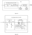
- Figure 1A shows a schematic circuit diagram of a TCU including an overvoltage protection circuit.
- Figure 1B-1C show two example circuit diagrams of the overvoltage protection circuit in a TCU shown in Figure 1A .
- an overvoltage protection circuit 100 is provided in front of each part of the circuit in the TCU or the internal power supply module of the TCU, the overvoltage protection circuit 100 includes an overvoltage protection unit 101 and a ⁇ -filter circuit 102 composed of inductors and capacitors (hereinafter referred to as the LC- ⁇ -filter circuit).
- Figure 1A shows the overvoltage protection circuit 100 located inside the TCU, according to the specific situation, the overvoltage protection circuit 100 can also be located outside the TCU.
- the overvoltage protection unit 101 can use a Zener diode for overvoltage protection, as shown in Figure 1B , by choosing the Zener diode of the appropriate specification, the high voltage appearing at the power input terminal of the TCU can be stabilized to its regulated value and provided to the input terminal of the internal power module of the TCU.
- the efficiency of Zener diodes is low, and they generate a large amount of heat.
- an overvoltage protection unit 101 based on an overvoltage protection control integrated circuit (IC) is also provided as shown in Figure 1C , the overvoltage protection unit 101 includes a switching transistor Q and an overvoltage protection control module 1011 (the control module includes a control integrated circuit IC).
- the overvoltage protection control integrated circuit IC controls the switching transistor Q to remain conductive, the overvoltage protection circuit directly outputs the input voltage signal of the power supply input terminal to the LC- ⁇ -filter circuit, then this is provided to the internal power module of the TCU, and when overvoltage is detected at the power input terminal of the TCU, the overvoltage protection control integrated circuit IC controls the switching transistor Q to become conductive and disconnected intermittently, similar to a voltage regulator.
- the voltage of the signal provided to the internal power supply module of the TCU through the LC- ⁇ -filter circuit is within the normal range.
- the overvoltage protection control integrated circuit IC controls the switching transistor Q to switch between the conductive and disconnected states, that is, when the switching transistor Q is made conductive and disconnected intermittently, since the first terminal of the switching transistor Q is connected to the input terminal of the overvoltage protection unit, the second terminal is connected to the output terminal of the overvoltage protection unit, that is, the input terminal of the LC- ⁇ -filter circuit; when the switching transistor Q is turned off, the input current signal of the LC-filter circuit will be zero, continuing until the switch is made conductive again, that is, the input current signal of the LC- ⁇ filter circuit will be discontinuous.
- the present invention provides an improved overvoltage protection circuit which can ensure that even if the input voltage of the signal input from the power supply (for example, the battery) to the power input terminal of the electric device (for example the TCU) is abnormally high (for example, an overvoltage appears at the power input terminal of the TCU during a load dump), the electrical apparatus can function normally, for example, the internal power module of the TCU can still work normally.
- the power supply for example, the battery
- the electric device for example the TCU
- Figure 2A shows a schematic circuit diagram of a TCU including an overvoltage protection circuit of an embodiment of the present invention.
- Figure 2B shows a schematic circuit diagram of an overvoltage protection circuit based on an embodiment of the present invention.
- the LC- ⁇ -filter circuit 202 is arranged in front of the overvoltage protection unit 201.
- the LC- ⁇ -filter circuit 202 is used to filter the input voltage signal to obtain a filtered voltage signal.
- the input terminal of the overvoltage protection unit 201 is connected to the output terminal of the LC- ⁇ -filter circuit, used to output the filtered voltage signal to serve as the output voltage signal of the overvoltage protection circuit or to adjust the filtered voltage signal to obtain an adjusted voltage signal as the output voltage signal of the overvoltage protection circuit, and to provide the output voltage signal to the internal power supply module of the TCU.
- the overvoltage protection unit 201 adjusts the filtered voltage signal
- the LC- ⁇ -filter circuit 202 supply of current to the overvoltage protection unit 201 is discontinuous, so an adjusted voltage signal with a sawtooth waveform is obtained. The specific process for this will be described in detail later.
- Figure 2B shows a further schematic circuit diagram of an overvoltage protection circuit 200 of an embodiment of the present invention.
- the LC- ⁇ -filter circuit 202 includes an inductor and two capacitors that are connected in a ⁇ -shape.
- the LC- ⁇ -filter circuit 202 receives the input voltage signal Vin from the power supply, and can filter the input voltage signal Vin to obtain the filtered voltage signal Vin_filtered.
- the input terminal of the overvoltage protection unit 201 receives the filtered voltage signal Vin_filtered, and generates an output voltage signal Vout of the overvoltage protection circuit based on the filtered voltage signal Vin_filtered.
- the overvoltage protection unit 201 directly uses the filtered voltage signal Vin_filtered as the output voltage signal Vout of the overvoltage protection circuit 300, and when it detects that the voltage value of the output voltage signal Vout is greater than or equal to a first threshold, the overvoltage protection unit 201 outputs an adjustment voltage signal Vp_out different from the filtered voltage signal as the output voltage signal Vout of the overvoltage protection circuit, wherein the voltage value of the adjusted voltage signal Vp_out is smaller than the first threshold and has a sawtooth waveform.
- maintaining the voltage of the output voltage signal Vout at less than the first threshold value may mean that the voltage of the output voltage signal Vout is less than a first threshold value within a predetermined time.
- the first threshold may be set according to the maximum input voltage allowed by the internal power supply module in the TCU unit.
- overvoltage protection unit 201 The structure of the overvoltage protection unit 201 will be described in detail below.
- the overvoltage protection unit includes a switching transistor Q and an output capacitor Cout, the first terminal of the switching transistor Q connects to the input terminal of the overvoltage protection unit 201, so as to receive the filtered voltage signal Vin_filtered, and the second terminal of switching transistor Q connects to the output terminal of the overvoltage protection unit 201 so when the voltage of the output voltage signal Vout is maintained at less than a first threshold, the voltage of the output filtered voltage signal Vin_filtered or output voltage signal Vout is greater than or equal to the first threshold, the adjusted voltage signal Vp_out is output; one terminal of output capacitor Cout connects to the second terminal of switching transistor Q, the other terminal of said output capacitor Cout is grounded.
- the switching transistor remains conductive when the voltage of the output voltage signal Vout remains less than the first threshold value, and intermittently becomes conductive and disconnected when the voltage of the output voltage signal Vout is greater than or equal to the first threshold.
- the first terminal of the switching transistor Q is connected to the input terminal of the overvoltage protection unit, that is, the output terminal of the LC- ⁇ -filter circuit
- the second terminal is connected to the output terminal of the overvoltage protection unit; when the switching transistor Q is turned off, the value of the output current signal from the LC- ⁇ -filter circuit to the overvoltage protection unit will be zero, continuing until the switching transistor is made conductive again, that is, the output current signal from the LC- ⁇ -filter circuit to the overvoltage protection unit will discontinuous. Therefore, the output capacitor Cout repeats the charging and discharging process as the switching transistor Q is made conductive and disconnected intermittently, so that said adjusted voltage signal Vp_out has a sawtooth waveform.
- the overvoltage protection unit 201 further includes an overvoltage protection control module 2011, and the overvoltage protection control module 2011 may be an overvoltage protection control integrated circuit IC.
- the control terminal of said switching transistor Q connects to said overvoltage protection control module 2011, and overvoltage protection control module 2011 is configured to: when the voltage Vout of the output voltage signal is maintained at less than a first threshold, the overvoltage protection control module operates in normal mode, so as to output an effective level control signal to the control terminal of switching transistor Q so as to maintain the conductive status of the switching transistor; and when the voltage Vout of the output voltage signal is maintained greater than or equal to a first threshold, operate in overvoltage protection mode, the overvoltage protection control module outputs an intermittent effective level control terminal to the control terminal of the switching transistor Q so as to intermittently make the switching transistor conductive and disconnected.
- the overvoltage protection unit 201 further includes a voltage detection circuit 2012, one terminal of said voltage detection circuit 2012 connects to the output terminal of the overvoltage protection unit 201, the other terminal of the voltage detection circuit 2012 is grounded, used for detecting the voltage of the output voltage signal Vout.
- the voltage detection circuit 2012 provides a voltage detection signal to the overvoltage protection control module 2011, and when the value of the voltage detection signal is greater than or equal to a first voltage detection threshold corresponding to the first threshold, the overvoltage protection control module enters the overvoltage protection mode, and controls the switching transistor to turn off until the value until the voltage detection signal drops to a predetermined ratio of the first voltage detection threshold, then controls the switching transistor to again become conductive until the value of the voltage detection signal is again greater than or equal to the corresponding first voltage detection threshold of the first threshold.
- an example of the voltage detection circuit 2012 includes a resistor divider circuit composed of resistors RF1 and RF2 in series; the ratio of the first voltage detection threshold to the first threshold is determined by the resistance values of RF1 and RF2.
- the overvoltage protection control module 2011 when the overvoltage protection control module 2011 operates in normal mode, as an example and not a limitation, the control signal of the effective level output by the overvoltage protection control module 2011 to the control terminal of the switching transistor Q can make the switching transistor Q fully conductive.
- the overvoltage protection control module operates in overvoltage mode 2011, the switching transistor Q needs to be switched from disconnected to conductive, in order to prevent the output capacitor Cout from being quickly charged to reach the first threshold again, an alternative method is that the overvoltage protection control module 2011 controls the switching transistor Q to be in an incompletely conductive state.
- the overvoltage protection control module 2011 outputs the intermittent effective level control signal to the control terminal of the switching transistor Q in overvoltage protection control mode.
- each effective level control signal acting on the control terminal of the switching transistor gradually increases, so that the voltage at the control terminal of the switching transistor Q gradually increases from a voltage value that makes the switching transistor work in an incompletely conductive state, therefore, the switching transistor Q remains incompletely conductive for a period of time, this ensures safe overvoltage protection.
- the overvoltage protection control module 2011 turns off the switching transistor by outputting a control signal of an invalid level, then, when it is detected that the value of the output voltage signal Vout has fallen to a predetermined proportion of the first threshold value, the overvoltage protection control module 2011 again makes the switching transistor Q conductive by acting on the level of the control terminal of the switching transistor via a control signal of the effective level, that is, at this time, the switch is controlled according to the gradually increasing voltage at the control terminal of the switching transistor gradually making the switching transistor Q conductive.
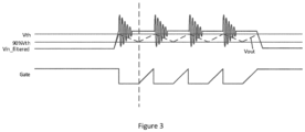
- the overvoltage protection circuit shown in Figure 2B when the overvoltage protection control module 2011 operates in overvoltage mode, the switching transistor is made conductive and disconnected intermittently, when the switching transistor Q is turned off, the LC- ⁇ -filter circuit does not supply current to the overvoltage protection, the inductance and capacitance inside the LC- ⁇ -filter circuit will form an oscillation loop, at this time, the voltage of the filtered voltage signal Vin_filtered will also appear as a voltage spike due to LC oscillation.
- the filtered voltage signal Vin_filtered with the voltage spike is only applied to the first terminal of the switching transistor Q, therefore it is only necessary to select the appropriate specifications of the switching transistor (for example, selecting a metal oxide semiconductor field effect transistor for which the maximum voltage it can withstand between the drain and source is greater than or equal to the voltage of the voltage spike), and the internal circuits of the overvoltage protection circuit (for example, switching transistors, overvoltage protection control modules, and voltage detection circuits) and subsequent circuits of the overvoltage protection circuit (for example, the internal power supply module of the TCU or directly connected control circuits or detection circuits, etc.) experience no overvoltage, thereby the subsequent circuits are provided with a voltage within the normal range that can ensure normal operation, and it is still possible to choose the subsequent circuits with lower input voltage even in the case of high input voltage, increasing the safety, adaptability and reliability of the overvoltage protection circuit.
- the overvoltage protection circuit for example, switching transistors, overvoltage protection control modules, and voltage detection circuits
- the overvoltage protection control module in the overvoltage protection unit 201 works in normal mode, so as to output an effective level control signal to switching transistor Q to maintain the conductive status of the switching transistor Q, so as to continue to directly output the filtered voltage signal Vin_filtered, serving as the output voltage signal of the overvoltage protection circuit, and the circuit has good electromagnetic compatibility performance.
- the overvoltage protection control module in the overvoltage protection unit 201 outputs an invalid level control signal to control the switching transistor Q to shut down. After the switching transistor is turned off, the output capacitor Cout starts to discharge so that the voltage on the output capacitor (that is, the voltage value of the output voltage signal Vout) starts to decrease.
- the overvoltage protection control module in the overvoltage protection unit 201 re-outputs an effective level control signal to drive the switching transistor to become conductive, in order to use the filtered voltage signal Vin_filtered to recharge the output capacitor Cout.
- the voltage on the output capacitor that is, the voltage of the output voltage signal Vout
- the effective level of the control signal output by the overvoltage protection control module acts on the level of control terminal at the switch tube to gradually increase, and at this time, the switching transistor is not directly completely conductive.
- the overvoltage protection control module in overvoltage protection unit 201 turns off the switching transistor Q again by outputting a control signal of an invalid level so as to stop charging the output capacitor Cout, so that the voltage on the output capacitor Cout again begins to gradually increase.
- the overvoltage protection control module in the overvoltage protection unit 201 causes the switching transistor to start to become conductive again by outputting a control signal of an effective level, and the turned on transistor is not fully conductive at this time, and it starts again charging the output capacitor, so that the voltage on the output capacitor gradually increases.
- the above process is repeated until the gradually increasing level at the control terminal of the switching transistor has made the switching transistor fully conductive, and at this time it is detected that the voltage value on the output capacitor remains less than the first threshold, the transistor remains fully conductive, thus, the filtered voltage signal Vin_filtered is directly output as the output voltage signal of the overvoltage protection circuit.
- the overvoltage protection control module in the overvoltage protection unit works in overvoltage protection mode, where the switching transistor is made conductive and disconnected intermittently, when the switching transistor is turned off, the LC of the LC- ⁇ -filter circuit will form an oscillation loop, at this time, the voltage of the filtered voltage signal Vin_filtered will also appear as a voltage spike due to LC oscillation.
- the voltage spike is interrupted by the switching transistor with appropriate specifications (for example, a metal oxide semiconductor field effect transistor with a maximum voltage that can be withstood between a suitable drain and source), and will not be transmitted to the output voltage signal Vout, as shown in Figure 3 .
- an overvoltage protection method based on the above-mentioned overvoltage protection circuit is also proposed.
- Figure 4 shows an overvoltage protection method according to an embodiment of the present invention.
- step 410 the LC- ⁇ -filter circuit filters the input voltage signal to obtain a filtered voltage signal.
- the overvoltage protection unit In step 420, the overvoltage protection unit generates an output voltage signal of the overvoltage protection circuit based on the filtered voltage signal, and when the voltage of the output voltage signal is greater than or equal to a first threshold, it outputs an adjusted voltage signal different to the filtered voltage signal to serve as the output voltage signal of the overvoltage protection circuit, the voltage of the adjusted voltage signal is less than the first threshold, wherein, the adjusted voltage signal has a sawtooth waveform.
- the above step 420 includes: control the switching transistor to remain conductive when the voltage of the output voltage signal remains less than a first threshold; and to intermittently become conductive and disconnected when the voltage of the output voltage signal is greater than or equal to the first threshold, and wherein, when the switching transistor is made conductive and disconnected intermittently, the output capacitor, repeats a charging and discharging process, so that the adjusted voltage signal has a sawtooth waveform.
- the above step 420 includes: when the voltage of the output voltage signal is maintained at less than a first threshold, causing the overvoltage protection module to operate in normal mode, so as to output an effective level control signal to the control terminal of switching transistor so as to maintain the conductive status of the switching transistor, and when the voltage of the output voltage signal is greater than or equal to a first threshold, causing said overvoltage protection module to operate in overvoltage protection mode, the overvoltage protection control module outputs an intermittent effective level control terminal to the control terminal of the switching transistor so as to intermittently make the switching transistor conductive and disconnected.
- the action of each effective level control signal of the intermittent effective level control signals on the control terminal of the switching transistor gradually increases.
- the above step 420 includes: causing the voltage detection circuit to provide a voltage detection signal to the overvoltage protection control module, and when the value of the voltage detection signal is greater than or equal to a first voltage detection threshold corresponding to the first threshold, the overvoltage protection control module that has entered overvoltage protection mode controls the switching transistor to be turned off until the value of the voltage detection signal drops to a predetermined ratio of the first voltage detection threshold, then it controls the switching transistor to again become conductive until the value of the voltage detection signal is again greater than or equal to the corresponding first voltage detection threshold of the first threshold, wherein, the switching transistor is controlled to be conductive based on the gradually increasing signal at the control terminal of the switching transistor.
- the above step 420 includes: when the overvoltage protection module operates in overvoltage protection mode, and when the switching transistor is fully conductive and the voltage of the output voltage signal is maintained at less than a first threshold, the overvoltage protection module switches to operate in normal mode.
- the LC- ⁇ -filter circuit is used to filter the input voltage signal to obtain a filtered voltage signal the overvoltage protection unit generates an output voltage signal of said overvoltage protection circuit based on said filtered voltage signal, and when the voltage of said output voltage signal is greater than or equal to a first threshold, it outputs an adjusted voltage signal different to said filtered voltage signal to serve as the output voltage signal of said overvoltage protection circuit, the voltage of the adjusted voltage signal is less than the first threshold, wherein, said adjusted voltage signal has a sawtooth waveform.
Landscapes
- Engineering & Computer Science (AREA)
- Power Engineering (AREA)
- Protection Of Static Devices (AREA)
- Dc-Dc Converters (AREA)
Claims (12)
- Überspannungsschutzschaltung (100), die Folgendes aufweist:eine Überspannungsschutzeinheit (101), die zum Erzeugen eines Ausgangsspannungssignals (Vout) der Überspannungsschutzschaltung verwendet wird, das auf einem gefilterten Spannungssignal basiert, und wenn die Spannung des Ausgangsspannungssignals größer als oder gleich einem ersten Schwellenwert (Vth) ist,gibt sie ein angepasstes Spannungssignal aus, das sich von dem gefilterten Spannungssignal unterscheidet und als Ausgangsspannungssignal der Überspannungsschutzschaltung dient, wobei die Spannung des angepassten Spannungssignals unter dem ersten Schwellenwert liegt,wobei das angepasste Spannungssignal eine Sägezahnwellenform aufweist,dadurch gekennzeichnet, dass die Überspannungsschutzschaltung ferner eine aus Induktoren und Kondensatoren zusammengesetzte n-Filterschaltung (202) enthält, die dazu dient, das Eingangsspannungssignal zu filtern, um das gefilterte Spannungssignal zu erhalten.
- Überspannungsschutzschaltung nach Anspruch 1, wobei die Überspannungsschutzeinheit einen Schalttransistor (Q) und einen Ausgangskondensator (Cout) enthält, ein erster Anschluss des Schalttransistors mit dem Eingangsanschluss der Überspannungsschutzeinheit verbunden ist, um das gefilterte Spannungssignal zu empfangen, ein zweiter Anschluss des Schalttransistors mit dem Ausgangsanschluss der Überspannungsschutzeinheit verbunden ist, um das gefilterte Spannungssignal oder das angepasste Spannungssignal auszugeben, ein Anschluss des Ausgangskondensators mit dem zweiten Anschluss des Schalttransistors verbunden ist, der andere Anschluss des Ausgangskondensators geerdet ist,wobei der Schalttransistor leitend bleibt, wenn die Spannung des Ausgangsspannungssignals kleiner als der erste Schwellenwert bleibt, und intermittierend leitend und abgeschaltet wird, wenn die Spannung des Ausgangsspannungssignals größer als oder gleich dem ersten Schwellenwert ist,wobei, wenn der Schalttransistor leitend ist und intermittierend abgeschaltet wird, der Ausgangskondensator einen Lade- und Entladevorgang wiederholt, so dass das angepasste Spannungssignal eine Sägezahnwellenform aufweist.
- Überspannungsschutzschaltung nach Anspruch 2, wobei die Überspannungsschutzeinheit ferner ein Überspannungsschutz-Steuermodul (2011) enthält, der Steueranschluss des Schalttransistors mit dem Überspannungsschutz-Steuermodul verbunden ist und das Überspannungsschutz-Steuermodul für Folgendes ausgebildet ist:wenn die Spannung des Ausgangsspannungssignals unter dem ersten Schwellenwert gehalten wird, arbeitet das Überspannungsschutz-Steuermodul im Normalmodus und gibt ein effektives Pegelsteuersignal an den Anschluss des Schalttransistors aus, um den leitenden Zustand des Schalttransistors aufrechtzuerhalten,wenn die Spannung des Ausgangsspannungssignals größer oder gleich dem ersten Schwellenwert ist, gibt das Überspannungsschutz-Steuermodul bei Betrieb des Überspannungsschutzmoduls ein intermittierendes effektives Pegelsteuersignal an den Anschluss des Schalttransistors aus, um den Schalttransistor intermittierend leitend und abschaltbar zu machen.
- Überspannungsschutzschaltung nach Anspruch 3, wobei die Wirkung jedes effektiven Pegelsteuersignals der intermittierenden effektiven Pegelsteuersignale auf den Steueranschluss des Schalttransistors allmählich zunimmt.
- Überspannungsschutzschaltung nach Anspruch 4, wobei die Überspannungsschutzeinheit ferner eine Spannungserkennungsschaltung (2012) enthält, ein Anschluss der Spannungserkennungsschaltung mit dem Ausgangsanschluss der Überspannungsschutzeinheit verbunden ist und der andere Anschluss der Spannungserkennungsschaltung geerdet ist,
wobei die Spannungserkennungsschaltung ein Spannungserkennungssignal an das Überspannungsschutz-Steuermodul liefert, und wenn der Wert des Spannungserkennungssignals größer oder gleich einem ersten Spannungserkennungsschwellenwert ist, der dem ersten Schwellenwert entspricht, das Überspannungsschutz-Steuermodul in den Überspannungsschutzmodus eintritt und den Schalttransistor steuert, um ihn auszuschalten, bis der Wert des Spannungserkennungssignals auf ein vorbestimmtes Verhältnis des ersten Spannungserkennungsschwellenwerts abfällt, dann den Schalttransistor so steuert, dass er wieder leitend wird, bis der Wert des Spannungserfassungssignals wieder größer oder gleich dem entsprechenden ersten Spannungserkennungsschwellenwert des ersten Schwellenwerts ist, wobei der Schalttransistor auf der Grundlage der allmählich ansteigenden Spannung am Steueranschluss des Schalttransistors so gesteuert wird, dass er leitend wird. - Überspannungsschutzschaltung nach Anspruch 5, wobei das Überspannungsschutz-Steuermodul ferner für Folgendes ausgebildet ist:
während des Betriebs im Überspannungsschutzmodus, wenn der Schalttransistor vollständig leitend ist und die Spannung des Ausgangsspannungssignals unter dem ersten Schwellenwert gehalten wird, Umschalten in den Normalmodus. - Verfahren zum Überspannungsschutz mit Anwendung der Überspannungsschutzschaltung nach einem der Ansprüche 1 bis 6, das folgendes beinhaltet:eine n-Filterschaltung (202), die aus Induktoren und Kondensatoren besteht, filtert das Eingangsspannungssignal, um ein gefiltertes Spannungssignal zu erhalten;eine Überspannungsschutzeinheit (201) erzeugt ein Ausgangsspannungssignal (Vout) der Überspannungsschutzschaltung basierend auf dem gefilterten Spannungssignal, und wenn die Spannung des Ausgangsspannungssignals größer als oder gleich einem ersten Schwellenwert (Vth) ist, gibt sie ein angepasstes Spannungssignal aus, das sich von dem gefilterten Spannungssignal unterscheidet, um als das Ausgangsspannungssignal der Überspannungsschutzschaltung zu dienen, wobei die Spannung des angepassten Spannungssignals kleiner als der erste Schwellenwert ist,wobei das angepasste Spannungssignal eine Sägezahnwellenform aufweist.
- Verfahren nach Anspruch 7, wobei die Überspannungsschutzeinheit einen Schalttransistor (Q) und einen Ausgangskondensator (Cout) enthält, ein erster Anschluss des Schalttransistors mit dem Eingangsanschluss der Überspannungsschutzeinheit verbunden ist, um das gefilterte Spannungssignal zu empfangen, ein zweiter Anschluss des Schalttransistors mit dem Ausgangsanschluss der Überspannungsschutzeinheit verbunden ist, um das gefilterte Spannungssignal oder das angepasste Spannungssignal auszugeben, ein Anschluss des Ausgangskondensators mit dem zweiten Anschluss des Schalttransistors verbunden ist, der andere Anschluss des Ausgangskondensators geerdet ist,
wobei die Überspannungsschutzeinheit ein Ausgangsspannungssignal der Überspannungsschutzschaltung basierend auf dem gefilterten Spannungssignal erzeugt, und wenn die Spannung des Ausgangsspannungssignals größer oder gleich dem ersten Schwellenwert ist, gibt sie ein angepasstes Spannungssignal aus, das sich von dem gefilterten Spannungssignal unterscheidet, um als das Ausgangsspannungssignal der Überspannungsschutzschaltung zu dienen, einschließlich:
Steuern des Schalttransistors, um leitend zu bleiben, wenn die Spannung des Ausgangsspannungssignals kleiner als der erste Schwellenwert bleibt; und um intermittierend leitend und ausgeschaltet zu werden, wenn die Spannung des Ausgangsspannungssignals größer als oder gleich dem ersten Schwellenwert ist, und wobei, wenn der Schalttransistor leitend gemacht und intermittierend ausgeschaltet wird, der Ausgangskondensator einen Lade- und Entladevorgang wiederholt, so dass das angepasste Spannungssignal eine Sägezahnwellenform hat. - Verfahren nach Anspruch 8, wobei die Überspannungsschutzeinheit ferner ein Überspannungsschutz-Steuermodul (2011) enthält und der Steueranschluss des Schalttransistors mit dem Überspannungsschutz-Steuermodul verbunden ist,
wobei die Überspannungsschutzeinheit ein Ausgangsspannungssignal der Überspannungsschutzschaltung basierend auf dem gefilterten Spannungssignal erzeugt, und wenn die Spannung des Ausgangsspannungssignals größer oder gleich dem ersten Schwellenwert ist, gibt sie ein angepasstes Spannungssignal aus, das sich von dem gefilterten Spannungssignal unterscheidet, um als das Ausgangsspannungssignal der Überspannungsschutzschaltung zu dienen, ferner Folgendes beinhaltend:wenn die Spannung des Ausgangsspannungssignals unter dem ersten Schwellenwert gehalten wird, das Überspannungsschutzmodul veranlasst, im Normalmodus zu arbeiten, um ein effektives Pegelsteuersignal an den Steueranschluss des Schalttransistors auszugeben, um den leitenden Zustand des Schalttransistors aufrechtzuerhalten,wenn die Spannung des Ausgangsspannungssignals größer oder gleich dem ersten Schwellenwert ist, arbeitet das Überspannungsschutzmodul im Überspannungsschutzmodus, so dass das Überspannungsschutz-Steuermodul ein intermittierendes effektives Pegelsteuersignal an den Steueranschluss des Schalttransistors ausgibt, um den Schalttransistor intermittierend leitend und ausgeschaltet zu machen. - Verfahren nach Anspruch 9, wobei die Wirkung jedes effektiven Pegelsteuersignals der intermittierenden effektiven Pegelsteuersignale auf den Steueranschluss des Schalttransistors allmählich zunimmt.
- Verfahren nach Anspruch 10, wobei die Überspannungsschutzeinheit eine Spannungserkennungsschaltung (2012) enthält, ein Anschluss der Spannungserkennungsschaltung mit dem Ausgangsanschluss der Überspannungsschutzeinheit verbunden ist und der andere Anschluss der Spannungserkennungsschaltung geerdet ist,
wobei die Überspannungsschutzeinheit ein Ausgangsspannungssignal der Überspannungsschutzschaltung basierend auf dem gefilterten Spannungssignal erzeugt, und wenn die Spannung des Ausgangsspannungssignals größer oder gleich dem ersten Schwellenwert ist, gibt sie ein angepasstes Spannungssignal aus, das sich von dem gefilterten Spannungssignal unterscheidet, um als das Ausgangsspannungssignal der Überspannungsschutzschaltung zu dienen, ferner Folgendes beinhaltend:
Bewirken, dass die Spannungserkennungsschaltung ein Spannungserkennungssignal an das Überspannungsschutz-Steuermodul liefert, und wenn der Wert des Spannungserkennungssignals größer oder gleich einem ersten Spannungserkennungsschwellenwert ist, der dem ersten Schwellenwert entspricht, steuert das Überspannungsschutz-Steuermodul, das in den Überspannungsschutzmodus eingetreten ist, dass der Schalttransistor ausgeschaltet wird, bis der Wert des Spannungserkennungssignals auf ein vorbestimmtes Verhältnis des ersten Spannungserkennungsschwellenwerts abfällt, dann den Schalttransistor so steuert, dass er wieder leitend wird, bis der Wert des Spannungserkennungssignals wieder größer oder gleich dem entsprechenden ersten Spannungserkennungsschwellenwert des ersten Schwellenwerts ist, wobei der Schalttransistor auf der Grundlage der allmählich ansteigenden Spannung am Steueranschluss des Schalttransistors so gesteuert wird, dass er leitend wird. - Verfahren nach Anspruch 11, wobei die Überspannungsschutzeinheit ein Ausgangsspannungssignal der Überspannungsschutzschaltung basierend auf dem gefilterten Spannungssignal erzeugt, und wenn die Spannung des Ausgangsspannungssignals größer oder gleich dem ersten Schwellenwert ist, gibt sie ein angepasstes Spannungssignal aus, das sich von dem gefilterten Spannungssignal unterscheidet, um als Ausgangsspannungssignal der Überspannungsschutzschaltung zu dienen, ferner Folgendes beinhaltend:
wenn das Überspannungsschutzmodul im Überspannungsschutzmodus arbeitet, wenn der Schalttransistor vollständig leitend ist und die Spannung des Ausgangsspannungssignals unter dem ersten Schwellenwert gehalten wird, schaltet das Überspannungsschutzmodul auf den Betrieb im Normalmodus um.
Applications Claiming Priority (1)
| Application Number | Priority Date | Filing Date | Title |
|---|---|---|---|
| CN201911069591.7A CN112769096B (zh) | 2019-11-05 | 2019-11-05 | 过压保护电路及过压保护方法 |
Publications (2)
| Publication Number | Publication Date |
|---|---|
| EP3820007A1 EP3820007A1 (de) | 2021-05-12 |
| EP3820007B1 true EP3820007B1 (de) | 2024-03-20 |
Family
ID=73834138
Family Applications (1)
| Application Number | Title | Priority Date | Filing Date |
|---|---|---|---|
| EP20205953.1A Active EP3820007B1 (de) | 2019-11-05 | 2020-11-05 | Überspannungsschutzschaltung und verfahren |
Country Status (2)
| Country | Link |
|---|---|
| EP (1) | EP3820007B1 (de) |
| CN (1) | CN112769096B (de) |
Families Citing this family (1)
| Publication number | Priority date | Publication date | Assignee | Title |
|---|---|---|---|---|
| CN119009881B (zh) * | 2024-08-13 | 2025-02-28 | 中家院(北京)检测认证有限公司 | 一种检测电网峰值自动切断电源方法及其系统 |
Family Cites Families (16)
| Publication number | Priority date | Publication date | Assignee | Title |
|---|---|---|---|---|
| US6590757B2 (en) * | 2001-09-28 | 2003-07-08 | Eaton Corporation | Method and apparatus for detecting and suppressing a parallel arc fault |
| CN101877545B (zh) * | 2009-04-30 | 2012-07-18 | 鸿富锦精密工业(深圳)有限公司 | 电源模块 |
| US8670219B2 (en) * | 2011-06-16 | 2014-03-11 | Monolithic Power Systems, Inc. | High-voltage devices with integrated over-voltage protection and associated methods |
| KR101424770B1 (ko) * | 2013-03-21 | 2014-08-01 | 최병규 | 전원 공급 장치 |
| CN203205848U (zh) * | 2013-04-18 | 2013-09-18 | 无锡中星微电子有限公司 | 电池保护电路 |
| CN103904875A (zh) * | 2014-03-24 | 2014-07-02 | 合肥工业大学 | 开关电源中的数字软启动电路 |
| CN204145300U (zh) * | 2014-10-28 | 2015-02-04 | 无锡中星微电子有限公司 | 一种升压dc/dc转换器 |
| CN104717772B (zh) * | 2015-03-16 | 2017-10-17 | 昂宝电子(上海)有限公司 | 用于电磁炉过流保护的控制电路和控制方法 |
| CN106329483B (zh) * | 2015-06-29 | 2018-11-09 | 欧姆龙株式会社 | 开关电源 |
| CN106786353A (zh) * | 2016-12-13 | 2017-05-31 | 京信通信技术(广州)有限公司 | 一种过压保护电路 |
| CN107204613B (zh) * | 2017-08-04 | 2019-01-15 | 郑州云海信息技术有限公司 | 一种过压保护装置及方法 |
| CN107681636A (zh) * | 2017-11-22 | 2018-02-09 | 合肥惠科金扬科技有限公司 | 一种过压保护电路以及开关电源 |
| CN108242888B (zh) * | 2018-01-16 | 2020-04-21 | 上海艾为电子技术股份有限公司 | 一种开环电荷泵 |
| CN208316271U (zh) * | 2018-04-16 | 2019-01-01 | 深圳和而泰智能控制股份有限公司 | 过压保护电路、控制板及用电设备 |
| CN209534784U (zh) * | 2019-02-14 | 2019-10-25 | 深圳市永联科技股份有限公司 | 充电桩及其充电模块 |
| CN109818328B (zh) * | 2019-03-19 | 2020-09-11 | 浪潮商用机器有限公司 | 一种开关电源过压保护电路 |
-
2019
- 2019-11-05 CN CN201911069591.7A patent/CN112769096B/zh active Active
-
2020
- 2020-11-05 EP EP20205953.1A patent/EP3820007B1/de active Active
Also Published As
| Publication number | Publication date |
|---|---|
| CN112769096B (zh) | 2026-04-28 |
| EP3820007A1 (de) | 2021-05-12 |
| CN112769096A (zh) | 2021-05-07 |
Similar Documents
| Publication | Publication Date | Title |
|---|---|---|
| US7586296B2 (en) | Power supply apparatus | |
| US11870241B2 (en) | Power control device | |
| CN102969887B (zh) | 车载用电源装置 | |
| US8629573B2 (en) | On-board electrical system for a motor vehicle, motor vehicle and method for operating an on-board electrical system | |
| CN104081641B (zh) | 车载用降压开关电源、车载用电子控制装置、以及怠速停止系统 | |
| US7282809B2 (en) | Interface circuit between a direct-current voltage source and a circuit for driving a load, particularly for use in motor-vehicles | |
| EP3820007B1 (de) | Überspannungsschutzschaltung und verfahren | |
| EP3157151B1 (de) | Elektronische steuerungsvorrichtung | |
| EP2665186B1 (de) | Elektronische steuervorrichtung zum steuern von lasttreibern durch mosfets | |
| US7110271B2 (en) | Inrush current prevention circuit for DC-DC converter | |
| CN212073944U (zh) | 电压转换装置和车辆 | |
| JP2005080336A (ja) | 車両用スイッチング電源装置 | |
| JP2020188643A (ja) | Dc/dcコンバータ | |
| US12263741B2 (en) | In-vehicle power supply device | |
| US12549177B2 (en) | Driving control device, vehicle-onboard power supply system, and vehicle | |
| CN114688008B (zh) | 一种汽车电子泵驱动控制电路和汽车电子模块 | |
| US20080111422A1 (en) | Voltage Regulator and Power System with a Voltage Boost for a Low Input Voltage | |
| WO2020022003A1 (ja) | 電子制御装置 | |
| JP2017017946A (ja) | 車両用電子制御装置 |
Legal Events
| Date | Code | Title | Description |
|---|---|---|---|
| PUAI | Public reference made under article 153(3) epc to a published international application that has entered the european phase |
Free format text: ORIGINAL CODE: 0009012 |
|
| STAA | Information on the status of an ep patent application or granted ep patent |
Free format text: STATUS: REQUEST FOR EXAMINATION WAS MADE |
|
| 17P | Request for examination filed |
Effective date: 20201105 |
|
| AK | Designated contracting states |
Kind code of ref document: A1 Designated state(s): AL AT BE BG CH CY CZ DE DK EE ES FI FR GB GR HR HU IE IS IT LI LT LU LV MC MK MT NL NO PL PT RO RS SE SI SK SM TR |
|
| GRAP | Despatch of communication of intention to grant a patent |
Free format text: ORIGINAL CODE: EPIDOSNIGR1 |
|
| STAA | Information on the status of an ep patent application or granted ep patent |
Free format text: STATUS: GRANT OF PATENT IS INTENDED |
|
| INTG | Intention to grant announced |
Effective date: 20230710 |
|
| P01 | Opt-out of the competence of the unified patent court (upc) registered |
Effective date: 20230629 |
|
| GRAS | Grant fee paid |
Free format text: ORIGINAL CODE: EPIDOSNIGR3 |
|
| GRAA | (expected) grant |
Free format text: ORIGINAL CODE: 0009210 |
|
| STAA | Information on the status of an ep patent application or granted ep patent |
Free format text: STATUS: THE PATENT HAS BEEN GRANTED |
|
| AK | Designated contracting states |
Kind code of ref document: B1 Designated state(s): AL AT BE BG CH CY CZ DE DK EE ES FI FR GB GR HR HU IE IS IT LI LT LU LV MC MK MT NL NO PL PT RO RS SE SI SK SM TR |
|
| REG | Reference to a national code |
Ref country code: GB Ref legal event code: FG4D |
|
| REG | Reference to a national code |
Ref country code: CH Ref legal event code: EP |
|
| REG | Reference to a national code |
Ref country code: DE Ref legal event code: R096 Ref document number: 602020027447 Country of ref document: DE |
|
| REG | Reference to a national code |
Ref country code: IE Ref legal event code: FG4D |
|
| PG25 | Lapsed in a contracting state [announced via postgrant information from national office to epo] |
Ref country code: LT Free format text: LAPSE BECAUSE OF FAILURE TO SUBMIT A TRANSLATION OF THE DESCRIPTION OR TO PAY THE FEE WITHIN THE PRESCRIBED TIME-LIMIT Effective date: 20240320 |
|
| REG | Reference to a national code |
Ref country code: LT Ref legal event code: MG9D |
|
| PG25 | Lapsed in a contracting state [announced via postgrant information from national office to epo] |
Ref country code: GR Free format text: LAPSE BECAUSE OF FAILURE TO SUBMIT A TRANSLATION OF THE DESCRIPTION OR TO PAY THE FEE WITHIN THE PRESCRIBED TIME-LIMIT Effective date: 20240621 |
|
| PG25 | Lapsed in a contracting state [announced via postgrant information from national office to epo] |
Ref country code: HR Free format text: LAPSE BECAUSE OF FAILURE TO SUBMIT A TRANSLATION OF THE DESCRIPTION OR TO PAY THE FEE WITHIN THE PRESCRIBED TIME-LIMIT Effective date: 20240320 Ref country code: RS Free format text: LAPSE BECAUSE OF FAILURE TO SUBMIT A TRANSLATION OF THE DESCRIPTION OR TO PAY THE FEE WITHIN THE PRESCRIBED TIME-LIMIT Effective date: 20240620 |
|
| REG | Reference to a national code |
Ref country code: NL Ref legal event code: MP Effective date: 20240320 |
|
| PG25 | Lapsed in a contracting state [announced via postgrant information from national office to epo] |
Ref country code: RS Free format text: LAPSE BECAUSE OF FAILURE TO SUBMIT A TRANSLATION OF THE DESCRIPTION OR TO PAY THE FEE WITHIN THE PRESCRIBED TIME-LIMIT Effective date: 20240620 Ref country code: NO Free format text: LAPSE BECAUSE OF FAILURE TO SUBMIT A TRANSLATION OF THE DESCRIPTION OR TO PAY THE FEE WITHIN THE PRESCRIBED TIME-LIMIT Effective date: 20240620 Ref country code: LT Free format text: LAPSE BECAUSE OF FAILURE TO SUBMIT A TRANSLATION OF THE DESCRIPTION OR TO PAY THE FEE WITHIN THE PRESCRIBED TIME-LIMIT Effective date: 20240320 Ref country code: HR Free format text: LAPSE BECAUSE OF FAILURE TO SUBMIT A TRANSLATION OF THE DESCRIPTION OR TO PAY THE FEE WITHIN THE PRESCRIBED TIME-LIMIT Effective date: 20240320 Ref country code: GR Free format text: LAPSE BECAUSE OF FAILURE TO SUBMIT A TRANSLATION OF THE DESCRIPTION OR TO PAY THE FEE WITHIN THE PRESCRIBED TIME-LIMIT Effective date: 20240621 Ref country code: FI Free format text: LAPSE BECAUSE OF FAILURE TO SUBMIT A TRANSLATION OF THE DESCRIPTION OR TO PAY THE FEE WITHIN THE PRESCRIBED TIME-LIMIT Effective date: 20240320 Ref country code: BG Free format text: LAPSE BECAUSE OF FAILURE TO SUBMIT A TRANSLATION OF THE DESCRIPTION OR TO PAY THE FEE WITHIN THE PRESCRIBED TIME-LIMIT Effective date: 20240320 |
|
| REG | Reference to a national code |
Ref country code: AT Ref legal event code: MK05 Ref document number: 1668686 Country of ref document: AT Kind code of ref document: T Effective date: 20240320 |
|
| PG25 | Lapsed in a contracting state [announced via postgrant information from national office to epo] |
Ref country code: SE Free format text: LAPSE BECAUSE OF FAILURE TO SUBMIT A TRANSLATION OF THE DESCRIPTION OR TO PAY THE FEE WITHIN THE PRESCRIBED TIME-LIMIT Effective date: 20240320 Ref country code: LV Free format text: LAPSE BECAUSE OF FAILURE TO SUBMIT A TRANSLATION OF THE DESCRIPTION OR TO PAY THE FEE WITHIN THE PRESCRIBED TIME-LIMIT Effective date: 20240320 |
|
| PG25 | Lapsed in a contracting state [announced via postgrant information from national office to epo] |
Ref country code: NL Free format text: LAPSE BECAUSE OF FAILURE TO SUBMIT A TRANSLATION OF THE DESCRIPTION OR TO PAY THE FEE WITHIN THE PRESCRIBED TIME-LIMIT Effective date: 20240320 |
|
| PG25 | Lapsed in a contracting state [announced via postgrant information from national office to epo] |
Ref country code: NL Free format text: LAPSE BECAUSE OF FAILURE TO SUBMIT A TRANSLATION OF THE DESCRIPTION OR TO PAY THE FEE WITHIN THE PRESCRIBED TIME-LIMIT Effective date: 20240320 |
|
| PG25 | Lapsed in a contracting state [announced via postgrant information from national office to epo] |
Ref country code: IS Free format text: LAPSE BECAUSE OF FAILURE TO SUBMIT A TRANSLATION OF THE DESCRIPTION OR TO PAY THE FEE WITHIN THE PRESCRIBED TIME-LIMIT Effective date: 20240720 |
|
| PG25 | Lapsed in a contracting state [announced via postgrant information from national office to epo] |
Ref country code: PT Free format text: LAPSE BECAUSE OF FAILURE TO SUBMIT A TRANSLATION OF THE DESCRIPTION OR TO PAY THE FEE WITHIN THE PRESCRIBED TIME-LIMIT Effective date: 20240722 Ref country code: SM Free format text: LAPSE BECAUSE OF FAILURE TO SUBMIT A TRANSLATION OF THE DESCRIPTION OR TO PAY THE FEE WITHIN THE PRESCRIBED TIME-LIMIT Effective date: 20240320 |
|
| PG25 | Lapsed in a contracting state [announced via postgrant information from national office to epo] |
Ref country code: ES Free format text: LAPSE BECAUSE OF FAILURE TO SUBMIT A TRANSLATION OF THE DESCRIPTION OR TO PAY THE FEE WITHIN THE PRESCRIBED TIME-LIMIT Effective date: 20240320 |
|
| PG25 | Lapsed in a contracting state [announced via postgrant information from national office to epo] |
Ref country code: EE Free format text: LAPSE BECAUSE OF FAILURE TO SUBMIT A TRANSLATION OF THE DESCRIPTION OR TO PAY THE FEE WITHIN THE PRESCRIBED TIME-LIMIT Effective date: 20240320 Ref country code: CZ Free format text: LAPSE BECAUSE OF FAILURE TO SUBMIT A TRANSLATION OF THE DESCRIPTION OR TO PAY THE FEE WITHIN THE PRESCRIBED TIME-LIMIT Effective date: 20240320 |
|
| PG25 | Lapsed in a contracting state [announced via postgrant information from national office to epo] |
Ref country code: AT Free format text: LAPSE BECAUSE OF FAILURE TO SUBMIT A TRANSLATION OF THE DESCRIPTION OR TO PAY THE FEE WITHIN THE PRESCRIBED TIME-LIMIT Effective date: 20240320 |
|
| PG25 | Lapsed in a contracting state [announced via postgrant information from national office to epo] |
Ref country code: PL Free format text: LAPSE BECAUSE OF FAILURE TO SUBMIT A TRANSLATION OF THE DESCRIPTION OR TO PAY THE FEE WITHIN THE PRESCRIBED TIME-LIMIT Effective date: 20240320 |
|
| PG25 | Lapsed in a contracting state [announced via postgrant information from national office to epo] |
Ref country code: SK Free format text: LAPSE BECAUSE OF FAILURE TO SUBMIT A TRANSLATION OF THE DESCRIPTION OR TO PAY THE FEE WITHIN THE PRESCRIBED TIME-LIMIT Effective date: 20240320 |
|
| PG25 | Lapsed in a contracting state [announced via postgrant information from national office to epo] |
Ref country code: SM Free format text: LAPSE BECAUSE OF FAILURE TO SUBMIT A TRANSLATION OF THE DESCRIPTION OR TO PAY THE FEE WITHIN THE PRESCRIBED TIME-LIMIT Effective date: 20240320 Ref country code: SK Free format text: LAPSE BECAUSE OF FAILURE TO SUBMIT A TRANSLATION OF THE DESCRIPTION OR TO PAY THE FEE WITHIN THE PRESCRIBED TIME-LIMIT Effective date: 20240320 Ref country code: RO Free format text: LAPSE BECAUSE OF FAILURE TO SUBMIT A TRANSLATION OF THE DESCRIPTION OR TO PAY THE FEE WITHIN THE PRESCRIBED TIME-LIMIT Effective date: 20240320 Ref country code: PT Free format text: LAPSE BECAUSE OF FAILURE TO SUBMIT A TRANSLATION OF THE DESCRIPTION OR TO PAY THE FEE WITHIN THE PRESCRIBED TIME-LIMIT Effective date: 20240722 Ref country code: PL Free format text: LAPSE BECAUSE OF FAILURE TO SUBMIT A TRANSLATION OF THE DESCRIPTION OR TO PAY THE FEE WITHIN THE PRESCRIBED TIME-LIMIT Effective date: 20240320 Ref country code: IS Free format text: LAPSE BECAUSE OF FAILURE TO SUBMIT A TRANSLATION OF THE DESCRIPTION OR TO PAY THE FEE WITHIN THE PRESCRIBED TIME-LIMIT Effective date: 20240720 Ref country code: ES Free format text: LAPSE BECAUSE OF FAILURE TO SUBMIT A TRANSLATION OF THE DESCRIPTION OR TO PAY THE FEE WITHIN THE PRESCRIBED TIME-LIMIT Effective date: 20240320 Ref country code: EE Free format text: LAPSE BECAUSE OF FAILURE TO SUBMIT A TRANSLATION OF THE DESCRIPTION OR TO PAY THE FEE WITHIN THE PRESCRIBED TIME-LIMIT Effective date: 20240320 Ref country code: CZ Free format text: LAPSE BECAUSE OF FAILURE TO SUBMIT A TRANSLATION OF THE DESCRIPTION OR TO PAY THE FEE WITHIN THE PRESCRIBED TIME-LIMIT Effective date: 20240320 Ref country code: AT Free format text: LAPSE BECAUSE OF FAILURE TO SUBMIT A TRANSLATION OF THE DESCRIPTION OR TO PAY THE FEE WITHIN THE PRESCRIBED TIME-LIMIT Effective date: 20240320 |
|
| PG25 | Lapsed in a contracting state [announced via postgrant information from national office to epo] |
Ref country code: IT Free format text: LAPSE BECAUSE OF FAILURE TO SUBMIT A TRANSLATION OF THE DESCRIPTION OR TO PAY THE FEE WITHIN THE PRESCRIBED TIME-LIMIT Effective date: 20240320 |
|
| REG | Reference to a national code |
Ref country code: DE Ref legal event code: R097 Ref document number: 602020027447 Country of ref document: DE |
|
| PG25 | Lapsed in a contracting state [announced via postgrant information from national office to epo] |
Ref country code: IT Free format text: LAPSE BECAUSE OF FAILURE TO SUBMIT A TRANSLATION OF THE DESCRIPTION OR TO PAY THE FEE WITHIN THE PRESCRIBED TIME-LIMIT Effective date: 20240320 |
|
| PG25 | Lapsed in a contracting state [announced via postgrant information from national office to epo] |
Ref country code: DK Free format text: LAPSE BECAUSE OF FAILURE TO SUBMIT A TRANSLATION OF THE DESCRIPTION OR TO PAY THE FEE WITHIN THE PRESCRIBED TIME-LIMIT Effective date: 20240320 |
|
| PLBE | No opposition filed within time limit |
Free format text: ORIGINAL CODE: 0009261 |
|
| STAA | Information on the status of an ep patent application or granted ep patent |
Free format text: STATUS: NO OPPOSITION FILED WITHIN TIME LIMIT |
|
| PG25 | Lapsed in a contracting state [announced via postgrant information from national office to epo] |
Ref country code: DK Free format text: LAPSE BECAUSE OF FAILURE TO SUBMIT A TRANSLATION OF THE DESCRIPTION OR TO PAY THE FEE WITHIN THE PRESCRIBED TIME-LIMIT Effective date: 20240320 |
|
| 26N | No opposition filed |
Effective date: 20241223 |
|
| PG25 | Lapsed in a contracting state [announced via postgrant information from national office to epo] |
Ref country code: SI Free format text: LAPSE BECAUSE OF FAILURE TO SUBMIT A TRANSLATION OF THE DESCRIPTION OR TO PAY THE FEE WITHIN THE PRESCRIBED TIME-LIMIT Effective date: 20240320 |
|
| REG | Reference to a national code |
Ref country code: CH Ref legal event code: PL |
|
| PG25 | Lapsed in a contracting state [announced via postgrant information from national office to epo] |
Ref country code: MC Free format text: LAPSE BECAUSE OF FAILURE TO SUBMIT A TRANSLATION OF THE DESCRIPTION OR TO PAY THE FEE WITHIN THE PRESCRIBED TIME-LIMIT Effective date: 20240320 |
|
| PG25 | Lapsed in a contracting state [announced via postgrant information from national office to epo] |
Ref country code: LU Free format text: LAPSE BECAUSE OF NON-PAYMENT OF DUE FEES Effective date: 20241105 |
|
| REG | Reference to a national code |
Ref country code: CH Ref legal event code: PL |
|
| GBPC | Gb: european patent ceased through non-payment of renewal fee |
Effective date: 20241105 |
|
| PG25 | Lapsed in a contracting state [announced via postgrant information from national office to epo] |
Ref country code: CH Free format text: LAPSE BECAUSE OF NON-PAYMENT OF DUE FEES Effective date: 20241130 |
|
| REG | Reference to a national code |
Ref country code: BE Ref legal event code: MM Effective date: 20241130 |
|
| PG25 | Lapsed in a contracting state [announced via postgrant information from national office to epo] |
Ref country code: BE Free format text: LAPSE BECAUSE OF NON-PAYMENT OF DUE FEES Effective date: 20241130 Ref country code: GB Free format text: LAPSE BECAUSE OF NON-PAYMENT OF DUE FEES Effective date: 20241105 |
|
| PG25 | Lapsed in a contracting state [announced via postgrant information from national office to epo] |
Ref country code: IE Free format text: LAPSE BECAUSE OF NON-PAYMENT OF DUE FEES Effective date: 20241105 |
|
| PGFP | Annual fee paid to national office [announced via postgrant information from national office to epo] |
Ref country code: DE Payment date: 20251117 Year of fee payment: 6 |
|
| PGFP | Annual fee paid to national office [announced via postgrant information from national office to epo] |
Ref country code: FR Payment date: 20251128 Year of fee payment: 6 |
|
| PG25 | Lapsed in a contracting state [announced via postgrant information from national office to epo] |
Ref country code: HU Free format text: LAPSE BECAUSE OF FAILURE TO SUBMIT A TRANSLATION OF THE DESCRIPTION OR TO PAY THE FEE WITHIN THE PRESCRIBED TIME-LIMIT; INVALID AB INITIO Effective date: 20201105 |
|
| PG25 | Lapsed in a contracting state [announced via postgrant information from national office to epo] |
Ref country code: CY Free format text: LAPSE BECAUSE OF FAILURE TO SUBMIT A TRANSLATION OF THE DESCRIPTION OR TO PAY THE FEE WITHIN THE PRESCRIBED TIME-LIMIT; INVALID AB INITIO Effective date: 20201105 |