EP3820124A1 - Funkfrequenzsystem, verfahren zur antennenumschaltung und entsprechendes produkt - Google Patents
Funkfrequenzsystem, verfahren zur antennenumschaltung und entsprechendes produkt Download PDFInfo
- Publication number
- EP3820124A1 EP3820124A1 EP19841769.3A EP19841769A EP3820124A1 EP 3820124 A1 EP3820124 A1 EP 3820124A1 EP 19841769 A EP19841769 A EP 19841769A EP 3820124 A1 EP3820124 A1 EP 3820124A1
- Authority
- EP
- European Patent Office
- Prior art keywords
- radio frequency
- coupled
- switch
- transmitting
- port
- Prior art date
- Legal status (The legal status is an assumption and is not a legal conclusion. Google has not performed a legal analysis and makes no representation as to the accuracy of the status listed.)
- Pending
Links
- 238000000034 method Methods 0.000 title claims abstract description 29
- 238000012545 processing Methods 0.000 claims abstract description 60
- 238000012546 transfer Methods 0.000 claims description 82
- 230000006870 function Effects 0.000 claims description 29
- 238000004891 communication Methods 0.000 claims description 14
- 238000004590 computer program Methods 0.000 claims description 10
- 238000013497 data interchange Methods 0.000 claims description 3
- 230000035945 sensitivity Effects 0.000 abstract description 11
- 230000010354 integration Effects 0.000 abstract description 7
- 230000008054 signal transmission Effects 0.000 description 12
- 230000005540 biological transmission Effects 0.000 description 9
- 238000010586 diagram Methods 0.000 description 8
- 238000010168 coupling process Methods 0.000 description 6
- 238000005859 coupling reaction Methods 0.000 description 6
- 238000003780 insertion Methods 0.000 description 6
- 230000037431 insertion Effects 0.000 description 6
- 230000009286 beneficial effect Effects 0.000 description 5
- 238000001514 detection method Methods 0.000 description 4
- 229920000106 Liquid crystal polymer Polymers 0.000 description 3
- 239000004977 Liquid-crystal polymers (LCPs) Substances 0.000 description 3
- 230000009471 action Effects 0.000 description 3
- 230000008878 coupling Effects 0.000 description 3
- 238000010295 mobile communication Methods 0.000 description 3
- 238000013461 design Methods 0.000 description 2
- 230000008569 process Effects 0.000 description 2
- 102000007530 Neurofibromin 1 Human genes 0.000 description 1
- 108010085793 Neurofibromin 1 Proteins 0.000 description 1
- 230000002776 aggregation Effects 0.000 description 1
- 238000004220 aggregation Methods 0.000 description 1
- 238000010276 construction Methods 0.000 description 1
- 238000005516 engineering process Methods 0.000 description 1
- 230000007774 longterm Effects 0.000 description 1
- 239000000463 material Substances 0.000 description 1
- 238000012986 modification Methods 0.000 description 1
- 230000004048 modification Effects 0.000 description 1
- 238000012360 testing method Methods 0.000 description 1
Images

Classifications
-
- H—ELECTRICITY
- H04—ELECTRIC COMMUNICATION TECHNIQUE
- H04B—TRANSMISSION
- H04B1/00—Details of transmission systems, not covered by a single one of groups H04B3/00 - H04B13/00; Details of transmission systems not characterised by the medium used for transmission
- H04B1/005—Details of transmission systems, not covered by a single one of groups H04B3/00 - H04B13/00; Details of transmission systems not characterised by the medium used for transmission adapting radio receivers, transmitters andtransceivers for operation on two or more bands, i.e. frequency ranges
- H04B1/0053—Details of transmission systems, not covered by a single one of groups H04B3/00 - H04B13/00; Details of transmission systems not characterised by the medium used for transmission adapting radio receivers, transmitters andtransceivers for operation on two or more bands, i.e. frequency ranges with common antenna for more than one band
- H04B1/006—Details of transmission systems, not covered by a single one of groups H04B3/00 - H04B13/00; Details of transmission systems not characterised by the medium used for transmission adapting radio receivers, transmitters andtransceivers for operation on two or more bands, i.e. frequency ranges with common antenna for more than one band using switches for selecting the desired band
-
- H—ELECTRICITY
- H04—ELECTRIC COMMUNICATION TECHNIQUE
- H04B—TRANSMISSION
- H04B7/00—Radio transmission systems, i.e. using radiation field
- H04B7/02—Diversity systems; Multi-antenna system, i.e. transmission or reception using multiple antennas
- H04B7/04—Diversity systems; Multi-antenna system, i.e. transmission or reception using multiple antennas using two or more spaced independent antennas
- H04B7/0404—Diversity systems; Multi-antenna system, i.e. transmission or reception using multiple antennas using two or more spaced independent antennas the mobile station comprising multiple antennas, e.g. to provide uplink diversity
-
- H—ELECTRICITY
- H04—ELECTRIC COMMUNICATION TECHNIQUE
- H04B—TRANSMISSION
- H04B1/00—Details of transmission systems, not covered by a single one of groups H04B3/00 - H04B13/00; Details of transmission systems not characterised by the medium used for transmission
- H04B1/02—Transmitters
- H04B1/03—Constructional details, e.g. casings, housings
- H04B1/034—Portable transmitters
-
- H—ELECTRICITY
- H04—ELECTRIC COMMUNICATION TECHNIQUE
- H04B—TRANSMISSION
- H04B1/00—Details of transmission systems, not covered by a single one of groups H04B3/00 - H04B13/00; Details of transmission systems not characterised by the medium used for transmission
- H04B1/02—Transmitters
- H04B1/04—Circuits
-
- H—ELECTRICITY
- H04—ELECTRIC COMMUNICATION TECHNIQUE
- H04B—TRANSMISSION
- H04B1/00—Details of transmission systems, not covered by a single one of groups H04B3/00 - H04B13/00; Details of transmission systems not characterised by the medium used for transmission
- H04B1/38—Transceivers, i.e. devices in which transmitter and receiver form a structural unit and in which at least one part is used for functions of transmitting and receiving
- H04B1/40—Circuits
- H04B1/401—Circuits for selecting or indicating operating mode
-
- H—ELECTRICITY
- H04—ELECTRIC COMMUNICATION TECHNIQUE
- H04B—TRANSMISSION
- H04B7/00—Radio transmission systems, i.e. using radiation field
- H04B7/02—Diversity systems; Multi-antenna system, i.e. transmission or reception using multiple antennas
- H04B7/04—Diversity systems; Multi-antenna system, i.e. transmission or reception using multiple antennas using two or more spaced independent antennas
- H04B7/0413—MIMO systems
-
- H—ELECTRICITY
- H04—ELECTRIC COMMUNICATION TECHNIQUE
- H04M—TELEPHONIC COMMUNICATION
- H04M1/00—Substation equipment, e.g. for use by subscribers
- H04M1/02—Constructional features of telephone sets
- H04M1/0202—Portable telephone sets, e.g. cordless phones, mobile phones or bar type handsets
- H04M1/026—Details of the structure or mounting of specific components
-
- H—ELECTRICITY
- H04—ELECTRIC COMMUNICATION TECHNIQUE
- H04B—TRANSMISSION
- H04B1/00—Details of transmission systems, not covered by a single one of groups H04B3/00 - H04B13/00; Details of transmission systems not characterised by the medium used for transmission
- H04B1/02—Transmitters
- H04B1/04—Circuits
- H04B2001/0408—Circuits with power amplifiers
-
- H—ELECTRICITY
- H04—ELECTRIC COMMUNICATION TECHNIQUE
- H04M—TELEPHONIC COMMUNICATION
- H04M1/00—Substation equipment, e.g. for use by subscribers
- H04M1/02—Constructional features of telephone sets
- H04M1/0202—Portable telephone sets, e.g. cordless phones, mobile phones or bar type handsets
- H04M1/026—Details of the structure or mounting of specific components
- H04M1/0277—Details of the structure or mounting of specific components for a printed circuit board assembly
-
- Y—GENERAL TAGGING OF NEW TECHNOLOGICAL DEVELOPMENTS; GENERAL TAGGING OF CROSS-SECTIONAL TECHNOLOGIES SPANNING OVER SEVERAL SECTIONS OF THE IPC; TECHNICAL SUBJECTS COVERED BY FORMER USPC CROSS-REFERENCE ART COLLECTIONS [XRACs] AND DIGESTS
- Y02—TECHNOLOGIES OR APPLICATIONS FOR MITIGATION OR ADAPTATION AGAINST CLIMATE CHANGE
- Y02D—CLIMATE CHANGE MITIGATION TECHNOLOGIES IN INFORMATION AND COMMUNICATION TECHNOLOGIES [ICT], I.E. INFORMATION AND COMMUNICATION TECHNOLOGIES AIMING AT THE REDUCTION OF THEIR OWN ENERGY USE
- Y02D30/00—Reducing energy consumption in communication networks
- Y02D30/70—Reducing energy consumption in communication networks in wireless communication networks
Definitions
- This disclosure relates to the field of mobile terminal technology, and particularly to a radio frequency system, a method for controlling antenna switching, and related products.
- the smart phone With the widespread use of electronic devices such as smart phones, the smart phone can support an increasing number of applications and is becoming more and more powerful. The smart phone is developing in a diversified and personalized way, becoming indispensable electronic products in users' life.
- the electronic device In the fourth generation (4G) mobile communication system, the electronic device generally adopts a single-antenna or dual-antenna radio frequency (RF) system architecture.
- RF radio frequency
- NR new radio
- Implementations provide a radio frequency system, a method for controlling antenna switching, and related products, to improve sensitivity of respective channels. Compared with a structure in which devices are separated, the degree of integration is higher and the area/cost/power consumption is optimized.
- implementations provide a radio frequency system.
- the radio frequency system supports a simultaneous downlink reception with four antennas and includes at least two antenna groups, a radio frequency processing circuit, and a radio frequency transceiver.
- the at least two antenna groups include m antennas, where m is greater than or equal to 4 and less than or equal to 8.
- the radio frequency processing circuit is coupled with the at least two antenna groups and includes modules which are the same in number as the at least two antenna groups. Each module is coupled with one antenna group and is disposed adjacent to the antenna group with which the module is coupled.
- the modules include one or more transmitting modules, or the modules include one or more transmitting modules and one or more receiving modules.
- the radio frequency transceiver is coupled with the radio frequency processing circuit.
- implementations provide an electronic device.
- the electronic device includes a radio frequency system.
- the radio frequency system supports a simultaneous downlink reception with four antennas and includes at least two antenna groups, a radio frequency processing circuit, and a radio frequency transceiver.
- the at least two antenna groups includes m antennas, where m is greater than or equal to 4 and less than or equal to 8.
- the radio frequency processing circuit is coupled with the at least two antenna groups and includes modules which are the same in number as the at least two antenna groups.
- the modules include one or more transmitting modules or one or more transmitting modules and one or more receiving modules. Each transmitting module is disposed adjacent to an antenna group with which the transmitting module is coupled, and each receiving module is disposed adjacent to an antenna group with which the receiving module is coupled.
- the radio frequency transceiver is coupled with the radio frequency processing circuit.
- the electronic device at least includes any of: a mobile terminal and a base station.
- implementations provide a method for controlling antenna switching.
- the method is applicable to an electronic device.
- the electronic device includes a radio frequency system.
- the radio frequency system includes a radio frequency transceiver, a radio frequency processing circuit coupled with the radio frequency transceiver, and at least two antenna groups coupled with the radio frequency processing circuit.
- the method includes the following. A transmitting path between a transmitting port in a target band of the radio frequency transceiver and a target antenna group in the radio frequency system is switched on, to transmit a signal through an antenna in the target antenna group.
- implementations provide a device for controlling antenna switching.
- the device is applicable to an electronic device.
- the electronic device includes a radio frequency system.
- the radio frequency system includes a radio frequency transceiver, a radio frequency processing circuit coupled with the radio frequency transceiver, and at least two antenna groups coupled with the radio frequency processing circuit.
- the device includes a processing unit and a communication unit.
- the processing unit is configured to, through the communication unit, switch on a transmitting path between a transmitting port in a target band of the radio frequency transceiver and a target antenna group in the radio frequency system, to transmit a signal through an antenna in the target antenna group.
- implementations provide an electronic device.
- the electronic device includes a processor, a memory, a communication interface, and one or more programs stored in the memory and configured to be executed by the processor.
- the one or more programs include instructions for performing operations of the method of the third aspect.
- implementations provide a computer readable storage medium.
- the computer readable storage medium is configured to store computer programs for electronic data interchange.
- the computer programs are operable with a computer to perform the method of the third aspect.
- the radio frequency system As respective modules of the radio frequency system are disposed adjacent to corresponding antenna groups and only the receiving module and the transmitting module are used to construct a central processing circuit, it is beneficial to improving sensitivity of various channels. Compared with a structure in which devices are separated, the degree of integration can be higher and the area/cost/power consumption can be optimized.
- the electronic device involved in the implementations may include various handheld devices, in-vehicle devices, wearable devices, computing devices that have wireless communication functions or other processing devices connected to the wireless modem, as well as various forms of user equipment (UE), mobile stations (MS), terminal devices, and the like.
- UE user equipment
- MS mobile stations
- terminal devices and the like.
- the above-mentioned devices are collectively referred to as an electronic device.
- SRS sounding reference signal
- CMCC China mobile communications corporation
- 5G Fifth Generation
- 3GPP 3rd generation partnership project
- a base station determines quality and parameters of four channels via measuring uplink (UL) signals of the four antennas of the mobile phone, to perform beamforming of a downlink optimal multi-input multi-output (MIMO) antenna array on the four channels according to a channel reciprocity, and finally to obtain the best data transmission performance for a downlink 4x4 MIMO.
- MIMO multi-input multi-output
- the electronic device may be a mobile phone or other terminal devices supporting the fifth generation new radio (5G NR), such as a customer premise equipment (CPE) or a mobile wireless-fidelity (MIFI).
- 5G NR fifth generation new radio
- CPE customer premise equipment
- MIFI mobile wireless-fidelity
- CD 5GNR requires downlink 4x4 MIMO or four-way diversity reception; 2 SRS switching in four antennas or transmitting (TX) an SRS with four antennas in turn (optional); 3 a function of switching among transmit antennas (optional); 4 the sub 6 GHz band ranges from 3.3 to 4.2G and 4.4 to 5G.
- This band has a higher frequency than the 600 ⁇ 2700MHz band of LTE (long term evolution). Therefore, the loss of the radio frequency (RF) cable (coaxial cable), from one side of a main board to the other side of the main board and from the main board to a secondary board (also called a lower board), is large.
- RF radio frequency
- K and T are fixed constants
- BW is determined by a tested bandwidth
- SNR is determined by the baseband algorithm of the system.
- NF NF 1 + NF 2 ⁇ 1 G 1 + ⁇ + NF i ⁇ 1 G 1 G 2 ⁇ G i ⁇ 1 + ⁇ + NF n ⁇ 1 G 1 G 2 ⁇ G n ⁇ 1
- NF 1 IL pre-1stLNA +NF 1st LNA , where IL pre-1st LNA is an insertion loss occurred before an LNA (low noise amplifier) in a first stage, and NF 1st LNA is a noise figure in the first stage. These two are main contributions of NF.
- NF 2 ⁇ 1 G 1 + ⁇ + NF i ⁇ 1 G 1 G 2 ⁇ G i ⁇ 1 + ⁇ + NF n ⁇ 1 G 1 G 2 ⁇ G n ⁇ 1 is the contribution of the noise figure in a latter stage.
- the radio frequency system for 5GNR is defined in the implementations.
- the receiving module and the transmitting module in the radio frequency system can be disposed adjacent to antennas, to reduce the insertion loss occurred before the LNA in the first stage and improve the sensitivity of the system.
- implementations provide a receiving module.
- the receiving module is applicable to a radio frequency system.
- the radio frequency system is operable in triple bands.
- the receiving module includes three signal receiving channels, a first transfer switch, and a second transfer switch.
- the first transfer switch is coupled with the three signal receiving channels.
- the three signal receiving channels are coupled with the second transfer switch.
- the first transfer switch includes (or is embodied as) a single-pole five-throw (SP5T) switch.
- the second transfer switch includes (or is embodied as) a single-pole quad-throw (SP4T) switch.
- Each of the three receiving channels includes a filter and a low noise amplifier (LNA), and the LNA is coupled with the filter.
- LNA low noise amplifier
- the first transfer switch is configured to be coupled with an antenna in an antenna group (also known as antenna array) corresponding to the receiving module.
- the second transfer switch is configured to be coupled with a transmitting module.
- the receiving module is disposed adjacent to the antenna group.
- the receiving module is integrated with the three signal receiving channels and is disposed adjacent to a corresponding antenna group, it is possible to reduce insertion loss of the link and beneficial to improving sensitivity of the channel. Compared with a structure in which devices are separated, the degree of integration is higher and the area/cost/power consumption is optimized.
- the receiving module further includes one internal Bypass channel, and the internal Bypass channel is disposed between the first transfer switch and the second transfer switch and is configured to be coupled with the transmitting module to support a signal transmitting function of the receiving module.
- the receiving module further includes one auxiliary port (AUX).
- the AUX is coupled with the first transfer switch and is configured to be coupled with the transmitting module to support the signal transmitting function of the receiving module. Compared with adopting an external Bypass channel, this structure can save one switch, thereby further reducing the insertion loss of the channel.
- the receiving module further includes two AUXs, i.e., a first AUX and a second AUX.
- the first AUX is coupled with the first transfer switch.
- the second AUX is coupled with the second transfer switch.
- An external Bypass channel is disposed between the first AUX and the second AUX and is configured to be coupled with the transmitting module to support the signal transmitting function of the receiving module.
- the receiving module further includes three AUXs, i.e., a first AUX, a second AUX, and a third AUX.
- the first AUX and the second AUX are coupled with the first transfer switch.
- the third AUX is coupled with the second transfer switch.
- the first AUX or the second AUX is configured to be coupled with the transmitting module to support the signal transmitting function of the receiving module.
- the first AUX and the third AUX or the second AUX and the third AUX are configured to be coupled with an external Bypass channel and the external Bypass channel is configured to be coupled with the transmitting module to support the signal transmitting function of the receiving module.
- the receiving module supports the signal transmitting function.
- the receiving module is disposed on a main board of an electronic device, and one AUX of the receiving module, which is coupled with the first transfer switch, is configured to be coupled with the transmitting module.
- the receiving module is disposed on a secondary board of the electronic device, and the first AUX or the second AUX is coupled with the third AUX
- NF of a receiving path can be reduced and sensitivity during receiving can be improved.
- the receiving module further includes the following features.
- the receiving module further includes a mobile industry processor interface (MIPI) control unit and/or a general-purpose input/output (GPIO) control unit.
- MIPI mobile industry processor interface
- GPIO general-purpose input/output
- the MIPI control unit and/or the GPIO control unit is configured to control devices in the receiving module.
- the devices include any one of: a first transfer switch and a second transfer switch.
- the receiving module includes three LNAs (including a first LNA, a second LNA, and a third LNA), three filters (including a first filter, a second filter, and a third filter), one AUX, two transfer switches (including a first transfer switch and a second transfer switch), and one internal Bypass channel.
- the first transfer switch is configured to be coupled with an antenna and includes an SP5T switch
- the second transfer switch is configured to be coupled with a radio frequency transceiver and/or a transmitting module and includes an SP4T switch.
- Nx, Ny, and Nz correspond to triple bands.
- the receiving module may also include an MIPI control unit and/or a GPIO control unit to achieve switching control of LNA/switch.
- the first transfer switch (including an SP3T switch) has a P port configured to be coupled with the antenna.
- the first transfer switch has a first T port coupled with the AUX.
- the first transfer switch has a second T port, a third T port, and a fourth T port that are respectively coupled with the first filter, the second filter, and the third filter.
- the first filter is coupled with the first LNA.
- the second filter is coupled with the second LNA.
- the third filter is coupled with the third LNA.
- the first LNA, the second LNA, and the third LNA are respectively coupled with a first T port, a second T port, and a third T port of the second transfer switch.
- the internal Bypass channel is disposed between a fifth T port of the first transfer switch and a fourth T port of the second transfer switch.
- the second transfer switch has a P port configured to be coupled with the transmitting module and/or the radio frequency transceiver.
- the receiving module includes three LNAs (including a first LNA, a second LNA, and a third LNA), three filters (including a first filter, a second filter, and a third filter), three AUXs (including a first AUX, a second AUX, and a third AUX), and two transfer switches (including a first transfer switch and a second transfer switch).
- the first AUX and the second AUX are coupled with the first transfer switch
- the third AUX is coupled with the second transfer switch.
- An external Bypass channel is configured to be disposed between the first AUX and the third AUX or between the second AUX and the third AUX to support a signal transmitting function of the receiving module.
- the first AUX or second AUX is configured to be coupled with a transmitting module to support the signal transmitting function of the receiving module.
- the first transfer switch is configured to be coupled with an antenna and includes an SP5T switch.
- the second transfer switch is configured to be coupled with a radio frequency transceiver and/or the transmitting module and includes an SP4T switch.
- Nx, Ny, and Nz correspond to triple bands.
- the receiving module may also include an MIPI control unit and/or a GPIO control unit to achieve switching control of LNA/switch.
- the first transfer switch has a P port configured to be coupled with the antenna.
- the first transfer switch has a first T port coupled with the first AUX.
- the first transfer switch has a second T port, a third T port, and a fourth T port that are coupled with the first filter, the second filter, and the third filter.
- the first filter is coupled with the first LNA.
- the second filter is coupled with the second LNA.
- the third filter is coupled with the third LNA.
- the first LNA, the second LNA, and the third LNA are coupled with a first T port, a second T port, and a third T port of the second transfer switch.
- the external Bypass channel is configured to be coupled between a fifth T port of the first transfer switch and a fourth T port of the second transfer switch.
- the second transfer switch has a P port configured to be coupled with the transmitting module.
- the receiving module can support switching of the signal transmitting function of the antenna through the internal Bypass channel or the external Bypass channel and the receiving module is disposed adjacent to the antenna group with which the receiving module is coupled, it is beneficial to improving sensitivity of various channels. Moreover, compared with a structure in which devices are separated, the integrated module has higher degree of integration and lower area/cost/power consumption.
- implementations provide a transmitting module.
- the transmitting module is applicable to a radio frequency system.
- the radio frequency system is operable in triple bands.
- the transmitting module includes three signal transmit-receive processing circuits, one power coupler, and two channel selector-switches (including a first channel selector-switch and a second channel selector-switch).
- the three signal transmit-receive processing circuits are coupled with the first channel selector-switch.
- the first channel selector-switch is coupled with the power coupler.
- the power coupler is coupled with the second channel selector-switch.
- the first channel selector-switch includes (or is embodied as) a single-pole triple-throw (SP3T) switch and the second channel selector-switch includes (or is embodied as) a quad-pole quad-throw (4P4T) switch and is a channel selector-switch in simplified connection.
- SP3T single-pole triple-throw
- 4P4T quad-pole quad-throw
- the second channel selector-switch is coupled with an antenna group corresponding to the transmitting module.
- the transmitting module is disposed adjacent to the antenna group.
- the channel selector-switch in simplified connection refers to a channel selector-switch including one or more non-full-coupling ports.
- the non-full-coupling port refers to a port that is not coupled with all peer ports. For example, in a 4P4T switch, a first T port can be coupled with all the four P ports but each of a second T port, a third T port, and a fourth T port can only be coupled with one P port.
- the transmitting module is integrated with the signal transmit-receive processing circuit and includes the channel selector-switch in simplified connection, it is possible to reduce the number of switches in the radio frequency (RF) link and insertion loss of the link and is beneficial to improving sensitivity of various channels. Compared with a structure in which devices are separated, degree of integration is higher and area/cost/power consumption is optimized.
- RF radio frequency
- the second channel selector-switch is coupled with the antenna group corresponding to the transmitting module.
- each signal transmit-receive processing circuit includes one power amplifier (PA), one LNA, one transmit-receive transfer switch, and one filter.
- the PA and the LNA are coupled with the transmit-receive transfer switch.
- the transmit-receive transfer switch is coupled with the filter.
- the three signal transmit-receive processing circuits are coupled with the first channel selector-switch.
- the first channel selector-switch is coupled with the power coupler.
- the power coupler is coupled with the second channel selector-switch.
- the transmit-receive transfer switch includes a single-pole double -throw (SPDT) switch.
- SPDT single-pole double -throw
- the PA of the signal transmit-receive processing circuit has an input port configured to be coupled with a signal transmitting port of a radio frequency transceiver.
- the LNA of the signal transmit-receive processing circuit has an output port configured to be coupled with a signal receiving port of the radio frequency transceiver.
- the power coupler is configured to be coupled with a power detection (PDET) port of the radio frequency transceiver.
- PDET power detection
- the first channel selector-switch and/or the second channel selector-switch has at least three ports served as external ports of the transmitting module, where one or two external ports of the external ports are configured to be coupled with an antenna(s) of the antenna group, and the rest of the external ports are configured to be coupled with a signal receiving port(s) of a receiving module, the radio frequency transceiver, and/or other transmitting modules.
- the transmitting module further includes an MIPI unit and/or a GPIO control unit.
- the MIPI control unit and/or the GPIO control unit is configured to control devices in the transmitting module.
- the device includes any one of: a transmit-receive transfer switch, a channel selector-switch, and a power detection selector-switch.
- the transmitting module includes three signal transmit-receive processing circuits, one power coupler, and two channel selector-switches (including a first channel selector-switch and a second channel selector-switch).
- Each signal transmit-receive processing circuit includes one PA, one LNA, one transmit-receive transfer switch (including an SPDT switch), and one filter.
- a first PA and a first LNA are coupled with a first transmit-receive transfer switch.
- the first transmit-receive transfer switch is coupled with a first filter.
- a second PA and a second LNA are coupled with a second transmit-receive transfer switch.
- the second transmit-receive transfer switch is coupled with a second filter.
- a third PA and a third LNA are coupled with a third transmit-receive transfer switch.
- the third transmit-receive transfer switch is coupled with a third filter.
- the first filter, the second filter, and the third filter are coupled with the first channel selector-switch, and the first channel selector-switch is coupled with the power coupler.
- the power coupler is coupled with the second channel selector-switch.
- the transmitting module can also include an MIPI control unit and/or a GPIO control unit to achieve switching control of LNA/switch.
- An input port of the first PA corresponds to a first external port of the transmitting module.
- An output port of the first LNA corresponds to a second external port of the transmitting module.
- An input port of the second PA corresponds to a third external port of the transmitting module.
- An output port of the second LNA corresponds to a fourth external port of the transmitting module.
- An input port of the third PA corresponds to a fifth external port of the transmitting module.
- An output port of the third LNA corresponds to a sixth external port of the transmitting module.
- a first P port, a second P port, a third P port, and a fourth P port of the second channel selector-switch correspond to a seventh external port, an eighth external port, a ninth external port, and a tenth external port of the transmitting module.
- a port of the power coupler corresponds to an eleventh external port of the transmitting module.
- a second T port, a third T port, and a fourth T port of the second channel selector-switch correspond to a twelfth external port, a thirteenth external port, and a fourteenth external port of the transmitting module.
- the first external port, the third external port, and the fifth external port are configured to be coupled with signal transmitting ports of a radio frequency transceiver.
- the seventh external port is configured to be coupled with an antenna of a corresponding antenna group.
- the eighth external port, the ninth external port, and the tenth external port are configured to be coupled with a receiving module or coupled with a receiving module and a transmitting module.
- the eleventh external port is configured to be coupled with a PDET port of the radio frequency transceiver.
- the external port(s) among the second external port, the fourth external port, the sixth external port, the twelfth external port, the thirteenth external port, and the fourteenth external port is configured to be coupled with a signal receiving port(s) of the radio frequency transceiver or a receiving port selector-switch.
- the external port(s) among the twelfth external port, the thirteenth external port, and the fourteenth external port is configured to be coupled with external ports of other transmitting modules.
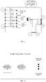
- a 5G radio frequency architecture supporting an electronic device is provided.
- the above receiving module and the transmitting module are applied to an electronic device.
- a radio frequency system includes a radio frequency transceiver, a radio frequency processing circuit, and at least two antenna groups.
- the radio frequency transceiver is coupled with the radio frequency processing circuit, and the radio frequency processing circuit is coupled with the at least two antenna groups.
- the radio frequency system supports a simultaneous downlink reception with four antennas.
- the at least two antenna groups include m antennas, and m is greater than or equal to 4 and less than or equal to 8.
- the radio frequency processing circuit includes multiple modules which are the same in number as the at least two antenna groups. Each module is coupled with one antenna group, and is disposed adjacent to the antenna group with which the module is coupled.
- the modules include one or more transmitting modules, or one or more transmitting modules and one or more receiving modules.
- the at least two antenna groups include four antenna groups (including a first antenna group, a second antenna group, a third antenna group, and a fourth antenna group), and the radio frequency processing circuit includes two transmitting modules (including a first transmitting module and a second transmitting module) and two receiving modules (including a first receiving module and a second receiving module).
- the first transmitting module is disposed adjacent to the first antenna group
- the second transmitting module is disposed adjacent to the second antenna group
- the first receiving module is disposed adjacent to the third antenna group
- the second receiving module is disposed adjacent to the fourth antenna group.
- the radio frequency processing circuit in the case that the radio frequency system supports a dual-transmit mode, includes two transmitting modules.
- the two transmitting modules are disposed on a main board.
- the at least two antenna groups include four antenna groups, and each antenna group includes one antenna.
- the radio frequency processing circuit further includes two receiving modules. The two receiving modules are disposed on a secondary board.
- the radio frequency transceiver is coupled with each transmitting module.
- Each transmitting module is coupled with one receiving module disposed on the secondary board to support signal receiving and transmitting functions of the receiving module, where the Bypass channel of the receiving module needs to be switched on to support the signal transmitting function.
- the radio frequency processing circuit further includes two receiving port selector-switches, each receiving port selector-switch is coupled with signal receiving ports of the radio frequency transceiver and a corresponding transmitting module, and the receiving port selector-switch includes an SP3T switch.
- the radio frequency architecture has the following function: CD supporting 5G NR triple bands; 2 not supporting UL CA; 3 not supporting DL CA; 4 supporting SRS switching in four antennas; 5 supporting NR 2T4R (two transmitting paths and four receiving paths in one band).
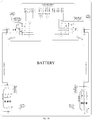
- the 5G radio frequency architecture includes a radio frequency transceiver, two transmitting modules, two receiving modules, two receiving port selector-switches (including a first receiving port selector-switch and a second receiving port selector-switch), and four antenna groups (including a first antenna group, a second antenna group, a third antenna group, and a fourth antenna group), where each antenna group includes one antenna.
- the radio frequency transceiver, the first transmitting module and the second transmitting module, and the first receiving port selector-switch and the second receiving port selector-switch are disposed on a main board (which is located above a battery in the figure).
- the first receiving module and the second receiving module are disposed on a secondary board (which is located below the battery in the figure).
- the first transmitting module is located adjacent to the first antenna group, the second transmitting module is located adjacent to the second antenna group, the first receiving module is located adjacent to the third antenna group, and the second receiving module is located adjacent to the fourth antenna group.
- the module is disposed adjacent to a feed point of an antenna with a relative distance ranging from 1-100 mm.
- a first T port of a second channel selector-switch of the first transmitting module is fully coupled with four P ports (that is, coupled with all the four P ports) of the second channel selector-switch of the first transmitting module.
- a first T port of a second channel selector-switch of the second transmitting module is fully coupled with four P ports (that is, coupled with all the four P ports) of the second channel selector-switch of the second transmitting module.
- a fourth T port of the second channel selector-switch of the first transmitting module is coupled with a fourth P port of the second channel selector-switch of the first transmitting module.
- a fourth T port of the second channel selector-switch of the second transmitting module is coupled with a fourth P port of the second channel selector-switch of the second transmitting module.
- a P port of a second transfer switch of the first receiving module is coupled with a tenth external port of the second transmitting module to support signal transmitting and receiving functions of the first receiving module.
- a P port of a second transfer switch of the second receiving module is coupled with a tenth external port of the first transmitting module to support signal transmitting and receiving functions of the second receiving module.
- the first receiving port selector-switch and the second receiving port selector-switch each include an SP3T switch.
- the first receiving port selector-switch is coupled with a fourteenth external port of the first transmitting module
- the second receiving port selector-switch is coupled with a fourteenth external port of the second transmitting module.
- a first transmitting port Nx TX1 in a first band of the radio frequency transceiver is coupled with a first external port of the first transmitting module.
- a first transmitting port Ny TX1 in a second band of the radio frequency transceiver is coupled with a third external port of the first transmitting module.
- a first transmitting port Nz TX1 in a third band of the radio frequency transceiver is coupled with a fifth external port of the first transmitting module.
- a second transmitting port Nx TX2 in the first band of the radio frequency transceiver is coupled with a first external port of the second transmitting module.
- a second transmitting port Ny TX2 in the second band of the radio frequency transceiver is coupled with a third external port of the second transmitting module.
- a second transmitting port Nz TX2 in the third band of the radio frequency transceiver is coupled with a fifth external port of the second transmitting module.
- a first receiving port Nx RX1 in the first band of the radio frequency transceiver is coupled with a second external port of the first transmitting module.
- a first receiving port Ny RX1 in the second band of the radio frequency transceiver is coupled with a fourth external port of the first transmitting module.
- a first receiving port Nz RX1 in the third band of the radio frequency transceiver is coupled with a sixth external port of the first transmitting module.
- a second receiving port Nx RX2 in the first band of the radio frequency transceiver is coupled with a second external port of the second transmitting module.
- a second receiving port Ny RX2 in the second band of the radio frequency transceiver is coupled with a fourth external port of the second transmitting module.
- a second receiving port Nz RX2 in the third band of the radio frequency transceiver is coupled with a sixth external port of the second transmitting module.
- a third receiving port Nx RX3 in the first band, a third receiving port Ny RX3 in the second band, and a third receiving port Nz RX3 in the third band of the radio frequency transceiver are respectively coupled with three T ports of the first receiving port selector-switch.
- a fourth receiving port Nx RX4 in the first band, a fourth receiving port Ny RX4 in the second band, and a fourth receiving port Nz RX4 in the third band of the radio frequency transceiver are respectively coupled with three T ports of the second receiving port selector-switch.
- a P port of the first receiving port selector-switch is coupled with the fourteenth external port of the first transmitting module.
- a P port of the second receiving port selector-switch is coupled with the fourteenth external port of the second transmitting module.
- a first power detection port PDET1 of the radio frequency transceiver is coupled with an eleventh external port of the first transmitting module.
- a second PDET2 is coupled with an eleventh external port of the second transmitting module.
- the first antenna group is coupled with a seventh external port of the first transmitting module.
- the second antenna group is coupled with a seventh external port of the second transmitting module.
- the third antenna group is coupled with a P port of a first transfer switch (including an SP3T switch) of the first receiving module.
- the fourth antenna group is coupled with a P port of a first transfer switch (including an SP3T switch) of the second receiving module.
- the radio frequency architecture described above is applied to an electronic device, and the electronic device switches on a transmitting path between a transmitting port in a target band of the radio frequency transceiver and a target antenna group in the radio frequency system, to transmit a signal through an antenna in the target antenna group.
- the electronic device including the foregoing radio frequency architecture performs SRS transmission with four antennas in turn or autonomous transmission switching as follows.
- the electronic device controls the first T port of the second channel selector-switch of the first transmitting module to be connected to a first P port of the second channel selector-switch of the first transmitting module, at the same time, controls the first T port of the second channel selector-switch of the first transmitting module to be connected to the fourth P port of the second channel selector-switch of the first transmitting module (corresponding to the tenth external port of the first transmitting module), and controls an internal Bypass channel of the second receiving module to be switched on, to realize signal transmission through antennas in the first antenna group and the fourth antenna group.
- the electronic device controls the first T port of the second channel selector-switch of the second transmitting module to be connected to a first P port of the second channel selector-switch of the second transmitting module (corresponding to the seventh external port of the second transmitting module), at the same time, controls the first T port of the second channel selector-switch of the second transmitting module to be connected to the fourth T port of the second channel selector-switch of the second transmitting module, and controls an internal Bypass channel of the first receiving module to be switched on, to realize signal transmission through antennas in the second antenna group and the third antenna group.
- the electronic device determines a signal transmission link of the target antenna group and controls the signal transmission link to be switched on, to achieve signal transmission through the antenna in the target antenna group.
- the signals include SRS TX signals or other signals, where other signals include various types of service data signals.
- the external ports of the transmitting module and the external ports of the receiving module of the implementation are extensible (that is, some external ports remain unconnected), for unification of modules to conveniently support various types of radio frequency systems.
- the external port of the transmitting module for connecting to the receiving module is not limited to the tenth external port and can be flexibly adjusted as required, which is not limited herein.
- the above-mentioned second channel selector-switch may have various simplified connection forms, for example, one T port is only connected to one P port, etc., which is not limited herein.
- the external port described in the implementations may be a port inherent to the internal device of the module, or may be an independent physical port extended with a wire, which is not limited herein.
- the internal ports of the above various nlPn2T (n1 is greater than or equal to 2, and n2 is greater than or equal to 2) switches (including any of the described channel selector-switch, power detection selector-switch, transmit-receive transfer switch, first transfer switch, second transfer switch, receiving port selector-switch, etc.) may be in full connection or simplified connection, and the connection between internal ports may be correspondingly set according to requirements.
- the first P port can be coupled only with the first T port, and the second P port can be coupled with three T ports.
- a switch with a full-coupling structure has an internal controllable circuit structure that can construct a path, such as construction and control through a switch transistor.
- coaxial cable in the radio frequency system described in the implementations may also be replaced by a liquid crystal polymer (LCP) material such as LCP soft board or the like.
- LCP liquid crystal polymer
- implementations provide an electronic device.
- the electronic device includes the radio frequency system according to any aspect of the foregoing implementations.
- the radio frequency system includes a radio frequency transceiver, a radio frequency processing circuit, and at least two antenna groups.
- the radio frequency transceiver is coupled with the radio frequency processing circuit, and the radio frequency processing circuit is coupled with the at least two antenna groups.
- the radio frequency system supports a simultaneous downlink reception with four antennas.
- the at least two antenna groups include m antennas, where m is greater than or equal to 4 and less than or equal to 8.
- the radio frequency processing circuit includes modules which are the same in number as the at least two antenna groups.
- the modules include one or more transmitting modules, or the modules include one or more transmitting modules and one or more receiving modules. Each transmitting module is disposed adjacent to the antenna group with which the transmitting module is coupled, and each receiving module is disposed adjacent to the antenna group with which the receiving module is coupled.
- the electronic device at least includes any of: a mobile terminal and a base station.
- implementations provide a method for controlling antenna switching.
- the method is applicable to the electronic device of the above implementations.
- the electronic device includes a radio frequency system.
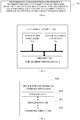
- the radio frequency system includes a radio frequency transceiver, a radio frequency processing circuit, and at least two antenna groups. As illustrated in FIG. 4 , the method begins at 401.
- the electronic device switches on a transmitting path between a transmitting port in a target band of the radio frequency transceiver and a target antenna group in the radio frequency system, to transmit a signal through an antenna in the target antenna group.
- the target band includes n79, n77, n41, and other bands in 5G NR, which is not limited herein.
- the transmitting port refers to the signal transmitting port of the radio frequency transceiver, and the target antenna group includes the first antenna group or the second antenna group or the third antenna group or the fourth antenna group.
- the signals include SRS TX signals or other signals.
- the electronic device can realize flexible switching of signal transmitting functions of the four antenna groups, meet 5G NR uplink switching requirements, and improve flexibility of signal transmission.
- the radio frequency system includes the radio frequency system of FIG. 3B .
- the electronic device including the foregoing radio frequency architecture performs SRS transmission with four antennas in turn or autonomous transmission switching as follows.
- the electronic device controls the first T port of the second channel selector-switch of the first transmitting module to be connected to a first P port of the second channel selector-switch of the first transmitting module, at the same time, controls the first T port of the second channel selector-switch of the first transmitting module to be connected to the fourth P port of the second channel selector-switch of the first transmitting module (corresponding to the tenth external port of the first transmitting module), and control an internal Bypass channel of the second receiving module to be switched on, to realize signal transmission through antennas in the first antenna group and the fourth antenna group.
- the electronic device controls the first T port of the second channel selector-switch of the second transmitting module to be connected to a first P port of the second channel selector-switch of the second transmitting module (corresponding to the seventh external port of the second transmitting module), at the same time, controls the first T port of the second channel selector-switch of the second transmitting module to be connected to the fourth T port of the second channel selector-switch of the second transmitting module, and controls an internal Bypass channel of the first receiving module to be switched on, to realize signal transmission through antennas in the second antenna group and the third antenna group.
- the electronic device determines a signal transmission link of the target antenna group and controls the signal transmission link to be switched on, to achieve signal transmission through the antenna in the target antenna group.
- the signals include SRS TX signals or other signals, where other signals include various types of service data signals.
- FIG. 5 is a schematic structural diagram illustrating the electronic device 500.
- the electronic device 500 includes an application processor 510, a memory 520 configured to store one or more programs 521, and a communication interface 530.
- the one or more programs 521 are configured to be executed by the application processor 510 and include instructions for performing the following.
- a transmitting path(s) between a transmitting port(s) in a target band of the radio frequency transceiver and a target antenna group(s) in the radio frequency system is switched on, to achieve signal transmission through an antenna(s) in the target antenna group(s).
- the electronic device can achieve switching between multiple transmit antennas, thus satisfying an antenna switching function in a multiple-antenna architecture.
- implementations provide a device for controlling antenna switching.
- the device for controlling antenna switching is applicable to the electronic device of the above implementations.
- the electronic device includes a radio frequency system.
- the radio frequency system includes a radio frequency transceiver, a radio frequency processing circuit, and at least two antenna groups.
- the device for controlling antenna switching includes a processing unit 601 and a communication unit 602.
- the processing unit 601 is configured to, through the communication unit 602, switch on a transmitting path between a transmitting port in a target band of the radio frequency transceiver and a target antenna group in the radio frequency system, to transmit a signal through an antenna in the target antenna group.
- the device for controlling antenna switching may further include a storage unit 603 for storing program codes and data of the electronic device.
- the processing unit 601 may be a processor.
- the communication unit 602 may be a touch screen display or a transceiver.
- the storage unit 603 may be a memory.
- the electronic device can achieve switching between multiple transmit antennas, thus satisfying an antenna switching function in a multiple-antenna architecture.
- Implementations also provide a computer readable storage medium.
- the computer readable storage medium is configured to store computer programs for electronic data interchange which, when executed, are operable with a computer to execute all or part of the operations of any of the methods described in the above-described method implementations.
- the computer may include an electronic device.
- Implementations also provide a computer program product.
- the computer program product includes a non-transitory computer readable storage medium that stores computer programs.
- the computer programs are operable with a computer to perform all or part of the operations of any of the methods described in the above method implementations.
- the computer program product may be a software installation package.
- the computer may include an electronic device.
- the apparatus disclosed in implementations provided herein may be implemented in other manners.
- the device/apparatus implementations described above are merely illustrative; for instance, the division of the unit is only a logical function division and there can be other manners of division during actual implementations, for example, multiple units or components may be combined or may be integrated into another system, or some features may be ignored, omitted, or not performed.
- coupling or communication connection between each illustrated or discussed component may be direct coupling or communication connection, or may be indirect coupling or communication among devices or units via some interfaces, and may be electrical connection, or other forms of connection.
- the units described as separate components may or may not be physically separated, the components illustrated as units may or may not be physical units, that is, they may be in the same place or may be distributed to multiple network elements. All or part of the units may be selected according to actual needs to achieve the purpose of the technical solutions of the implementations.
- the functional units in various implementations may be integrated into one processing unit, or each unit may be physically present, or two or more units may be integrated into one unit.
- the above-mentioned integrated unit can be implemented in the form of hardware or a software function unit.
- the integrated unit may be stored in a computer-readable memory when it is implemented in the form of a software functional unit and is sold or used as a separate product.
- the technical solutions essentially, or the part of the technical solutions that contributes to the related art, or all or part of the technical solutions may be embodied in the form of a software product which is stored in a memory and includes instructions for causing a computer device (which may be a personal computer, a server, or a network device and so on) to perform all or part of the steps described in the various implementations.
- the memory includes various medium capable of storing program codes, such as a USB (universal serial bus) flash disk, a read-only memory (ROM), a random-access memory (RAM), a removable hard disk, Disk, compact disc (CD), or the like.
Landscapes
- Engineering & Computer Science (AREA)
- Signal Processing (AREA)
- Computer Networks & Wireless Communication (AREA)
- Transceivers (AREA)
- Mobile Radio Communication Systems (AREA)
Applications Claiming Priority (3)
| Application Number | Priority Date | Filing Date | Title |
|---|---|---|---|
| CN201810811718 | 2018-07-23 | ||
| CN201810828093.5A CN108965533B (zh) | 2018-07-23 | 2018-07-25 | 射频系统、天线切换控制方法及相关产品 |
| PCT/CN2019/089887 WO2020019874A1 (zh) | 2018-07-23 | 2019-06-03 | 射频系统、天线切换控制方法及相关产品 |
Publications (2)
| Publication Number | Publication Date |
|---|---|
| EP3820124A1 true EP3820124A1 (de) | 2021-05-12 |
| EP3820124A4 EP3820124A4 (de) | 2021-08-18 |
Family
ID=64322639
Family Applications (1)
| Application Number | Title | Priority Date | Filing Date |
|---|---|---|---|
| EP19841769.3A Pending EP3820124A4 (de) | 2018-07-23 | 2019-06-03 | Funkfrequenzsystem, verfahren zur antennenumschaltung und entsprechendes produkt |
Country Status (4)
| Country | Link |
|---|---|
| US (1) | US11431356B2 (de) |
| EP (1) | EP3820124A4 (de) |
| CN (21) | CN108988875B (de) |
| WO (5) | WO2020019877A1 (de) |
Cited By (3)
| Publication number | Priority date | Publication date | Assignee | Title |
|---|---|---|---|---|
| EP4142164A4 (de) * | 2020-05-26 | 2023-10-25 | Guangdong Oppo Mobile Telecommunications Corp., Ltd. | Hochfrequenz-pa-mid-vorrichtung, hochfrequenz-sendeempfangssystem und kommunikationsvorrichtung |
| EP4258562A4 (de) * | 2020-12-16 | 2024-05-01 | Guangdong Oppo Mobile Telecommunications Corp., Ltd. | Funkfrequenzsendeempfangssystem und kommunikationsvorrichtung |
| EP4401321A4 (de) * | 2021-09-30 | 2024-11-13 | Huawei Technologies Co., Ltd. | Funkfrequenz-frontendmodul, funkfrequenzvorrichtung und kommunikationsvorrichtung |
Families Citing this family (67)
| Publication number | Priority date | Publication date | Assignee | Title |
|---|---|---|---|---|
| CN108988875B (zh) * | 2018-07-23 | 2020-12-08 | Oppo广东移动通信有限公司 | 射频系统、天线切换控制方法及相关产品 |
| CN109634513A (zh) * | 2018-12-29 | 2019-04-16 | 出门问问信息科技有限公司 | 触摸功能的控制方法及装置 |
| CN109951207A (zh) * | 2019-03-20 | 2019-06-28 | Oppo广东移动通信有限公司 | 射频系统及电子设备 |
| CN114665940B (zh) * | 2019-03-28 | 2025-11-11 | Oppo广东移动通信有限公司 | 射频系统、天线切换控制方法、相关设备及存储介质 |
| CN112054312B (zh) * | 2019-06-06 | 2022-10-18 | 北京小米移动软件有限公司 | 天线结构和电子设备 |
| CN110176940B (zh) * | 2019-06-14 | 2021-04-13 | Oppo广东移动通信有限公司 | 射频电路及电子设备 |
| CN112152643B (zh) | 2019-06-28 | 2022-03-11 | 华为技术有限公司 | 一种天线的切换电路和电子设备 |
| CN110224712B (zh) * | 2019-07-08 | 2021-04-23 | Oppo广东移动通信有限公司 | 射频电路、电子设备及射频电路控制方法 |
| CN110149132B (zh) * | 2019-07-08 | 2021-07-20 | 维沃移动通信有限公司 | 一种发射天线的切换方法及终端设备 |
| CN110535483B (zh) * | 2019-07-26 | 2021-01-15 | 华为技术有限公司 | 通信模块及终端 |
| CN110830055B (zh) * | 2019-10-30 | 2021-11-16 | 西安广和通无线通信有限公司 | 天线模组及天线适配方法 |
| CN111064491B (zh) * | 2019-12-03 | 2021-06-15 | 青岛海信移动通信技术股份有限公司 | 一种移动终端设备及其收发信号的方法 |
| JP7556966B2 (ja) * | 2019-12-31 | 2024-09-26 | 華為技術有限公司 | 通信装置およびネットワークデバイス |
| CN116761281A (zh) * | 2020-01-21 | 2023-09-15 | Oppo广东移动通信有限公司 | 客户前置设备 |
| CN111277299A (zh) * | 2020-01-21 | 2020-06-12 | Oppo广东移动通信有限公司 | 用户终端设备 |
| CN111277314B (zh) * | 2020-01-21 | 2023-12-19 | Oppo广东移动通信有限公司 | 一种天线选路方法及相关装置 |
| CN111277298B (zh) * | 2020-01-21 | 2021-11-09 | Oppo广东移动通信有限公司 | 客户前置设备 |
| CN111245482B (zh) * | 2020-01-21 | 2021-11-05 | Oppo广东移动通信有限公司 | 一种天线选路方法及相关装置 |
| CN111294081B (zh) | 2020-01-22 | 2022-01-11 | Oppo广东移动通信有限公司 | 射频系统和电子设备 |
| CN111342847B (zh) * | 2020-02-13 | 2021-11-30 | 芯朴科技(上海)有限公司 | 调整输出功率的方法 |
| CN113746496B (zh) * | 2020-03-03 | 2022-07-08 | Oppo广东移动通信有限公司 | 射频系统及电子设备 |
| CN111600625A (zh) * | 2020-05-14 | 2020-08-28 | 锐石创芯(深圳)科技有限公司 | 射频前端电路和射频前端装置 |
| WO2021238430A1 (zh) * | 2020-05-26 | 2021-12-02 | Oppo广东移动通信有限公司 | 射频PA Mid器件、射频系统和通信设备 |
| CN113726357A (zh) * | 2020-05-26 | 2021-11-30 | Oppo广东移动通信有限公司 | 射频PA Mid器件、射频收发系统和通信设备 |
| CN111682885B (zh) * | 2020-06-09 | 2022-10-04 | 芯朴科技(上海)有限公司 | 1t2r射频电路、无线通信设备 |
| CN111756388B (zh) * | 2020-06-28 | 2022-06-07 | 维沃移动通信有限公司 | 一种射频电路及电子设备 |
| CN111800161B (zh) * | 2020-06-30 | 2022-08-19 | 联想(北京)有限公司 | 一种电子设备 |
| CN113972940B (zh) * | 2020-07-22 | 2025-08-05 | 中兴通讯股份有限公司 | 频分双工系统的探测参考信号传输方法及终端 |
| CN111817745B (zh) * | 2020-07-28 | 2022-08-05 | 惠州Tcl移动通信有限公司 | 射频装置及移动终端 |
| CN112152649B (zh) * | 2020-09-16 | 2022-04-12 | Oppo广东移动通信有限公司 | 射频电路、终端设备、信号传输方法及存储介质 |
| CN112152690B (zh) * | 2020-09-18 | 2024-02-09 | Oppo广东移动通信有限公司 | 分集接收装置、设备、方法和计算机可读存储介质 |
| CN112187311B (zh) * | 2020-09-27 | 2022-08-09 | Oppo广东移动通信有限公司 | 射频系统和通信设备 |
| CN112383321B (zh) * | 2020-11-12 | 2022-05-13 | Oppo广东移动通信有限公司 | 射频系统、天线切换控制方法和客户前置设备 |
| CN112468178B (zh) * | 2020-11-27 | 2022-08-09 | Oppo广东移动通信有限公司 | 射频系统、天线切换方法和客户前置设备 |
| CN112564731B (zh) * | 2020-12-03 | 2022-03-25 | 维沃移动通信有限公司 | 信号处理电路、方法和电子设备 |
| CN114640369B (zh) * | 2020-12-16 | 2023-03-24 | Oppo广东移动通信有限公司 | 射频收发系统及通信设备 |
| CN114640359B (zh) * | 2020-12-16 | 2023-08-29 | Oppo广东移动通信有限公司 | 射频PA Mid器件、射频收发系统和通信设备 |
| CN114640358B (zh) * | 2020-12-16 | 2023-10-03 | Oppo广东移动通信有限公司 | 射频PA Mid器件、射频收发系统和通信设备 |
| CN114759943B (zh) * | 2020-12-29 | 2023-06-02 | 华为技术有限公司 | 射频前端模块、以及控制射频前端模块的方法和装置 |
| CN112751578B (zh) * | 2021-01-06 | 2023-05-05 | Oppo广东移动通信有限公司 | 射频elna器件和射频系统 |
| CN112886980B (zh) * | 2021-01-22 | 2022-06-10 | 维沃移动通信有限公司 | 射频电路和电子设备 |
| CN114915301B (zh) * | 2021-02-09 | 2023-09-05 | 北京小米移动软件有限公司 | 天线模组、终端设备、天线调节方法及装置 |
| CN115118297B (zh) * | 2021-03-18 | 2023-11-10 | Oppo广东移动通信有限公司 | 射频前端模组、射频收发系统和通信设备 |
| CN115765762B (zh) * | 2021-03-30 | 2024-02-13 | Oppo广东移动通信有限公司 | 射频组件和通信设备 |
| CN113472386A (zh) * | 2021-06-30 | 2021-10-01 | 展讯通信(上海)有限公司 | 天线模组、控制方法和装置 |
| CN113765527A (zh) * | 2021-07-23 | 2021-12-07 | 上海闻泰信息技术有限公司 | 一种分频器和分频器的控制方法 |
| CN113489555B (zh) * | 2021-08-10 | 2023-04-18 | 上海闻泰信息技术有限公司 | 信道质量检测终端及电子设备 |
| CN113676193B (zh) * | 2021-08-12 | 2022-11-11 | Oppo广东移动通信有限公司 | 发射模组、射频系统及通信设备 |
| CN113676212B (zh) * | 2021-08-12 | 2022-07-15 | Oppo广东移动通信有限公司 | 放大器模组、射频系统及通信设备 |
| CN113676210B (zh) * | 2021-08-12 | 2022-07-15 | Oppo广东移动通信有限公司 | 放大器模组、射频系统及通信设备 |
| CN113676192B (zh) * | 2021-08-12 | 2023-01-06 | Oppo广东移动通信有限公司 | 发射模组、射频系统及通信设备 |
| CN113676207B (zh) * | 2021-08-12 | 2022-12-27 | Oppo广东移动通信有限公司 | 发射模组、射频系统及通信设备 |
| CN113676213B (zh) * | 2021-08-12 | 2022-07-15 | Oppo广东移动通信有限公司 | 放大器模组、射频系统及通信设备 |
| CN113676191B (zh) * | 2021-08-12 | 2022-12-27 | Oppo广东移动通信有限公司 | 发射模组、射频系统及通信设备 |
| CN113938152B (zh) * | 2021-11-30 | 2022-12-13 | Oppo广东移动通信有限公司 | 射频系统及通信设备 |
| CN114244394B (zh) * | 2021-11-30 | 2022-10-21 | 荣耀终端有限公司 | 射频前端模块、终端设备以及射频前端模块的控制方法 |
| CN114675245B (zh) * | 2022-04-21 | 2024-11-15 | 中国科学院空天信息创新研究院 | 一种收发定标组件的设计装置及方法 |
| CN115065379A (zh) * | 2022-05-18 | 2022-09-16 | Oppo广东移动通信有限公司 | 射频开关、射频系统和通信设备 |
| CN114745034B (zh) * | 2022-06-13 | 2022-09-20 | 合肥龙旗智能科技有限公司 | 射频模组、信号收发方法及无线通信设备 |
| CN115037317B (zh) * | 2022-06-24 | 2023-11-10 | Oppo广东移动通信有限公司 | 射频lfem器件、射频系统和通信设备 |
| CN115133950B (zh) * | 2022-06-29 | 2024-03-26 | 联想(北京)有限公司 | 一种信号收发电路、测量方法及装置 |
| CN115499041A (zh) * | 2022-11-14 | 2022-12-20 | 深圳芯盛思技术有限公司 | 一种采用相控阵技术的客户端设备 |
| CN115776304B (zh) * | 2023-02-07 | 2023-05-12 | 唯捷创芯(天津)电子技术股份有限公司 | 一种低损耗的射频收发前端模块及电子设备 |
| US20240322992A1 (en) * | 2023-03-23 | 2024-09-26 | Wilson Electronics, Llc | Repeater Switchable Between a Duplex Mode and a Simplex Mode |
| CN118868995B (zh) * | 2024-07-10 | 2025-06-13 | 睿思微系统(烟台)有限公司 | 一种通信装置,射频系统以及射频前端模块 |
| CN119051695B (zh) * | 2024-07-12 | 2025-02-25 | 北京唯得科技有限公司 | 基站天线和5g mimo移频双路双天线系统 |
| CN118764044B (zh) * | 2024-09-06 | 2025-03-14 | 荣耀终端股份有限公司 | 射频电路、功率控制方法和电子设备 |
Family Cites Families (48)
| Publication number | Priority date | Publication date | Assignee | Title |
|---|---|---|---|---|
| US6819938B2 (en) * | 2001-06-26 | 2004-11-16 | Qualcomm Incorporated | System and method for power control calibration and a wireless communication device |
| CN101854198B (zh) * | 2009-03-30 | 2014-01-01 | 中兴通讯股份有限公司南京分公司 | 一种多天线发射分集的方法和装置 |
| CN101572939B (zh) * | 2009-05-27 | 2011-12-21 | 上海华为技术有限公司 | 射频模块、收发信机及收发信机切换控制的方法 |
| CN101800566B (zh) | 2010-01-06 | 2015-09-09 | 华为终端有限公司 | 一种射频前端系统 |
| US8838042B2 (en) * | 2010-05-21 | 2014-09-16 | Marvell World Trade Ltd. | RF front-end with integrated T/R switch |
| US8666328B2 (en) * | 2010-07-12 | 2014-03-04 | Apple Inc. | Wireless circuitry with reduced harmonic interference |
| CN202103661U (zh) | 2011-07-15 | 2012-01-04 | 惠州市正源微电子有限公司 | 多模多频手机射频前端模块 |
| JP6032543B2 (ja) * | 2012-10-19 | 2016-11-30 | パナソニックIpマネジメント株式会社 | アンテナ切り替え受信システム及びそれに対応する送信システム |
| US9468022B2 (en) * | 2012-12-26 | 2016-10-11 | Samsung Electronics Co., Ltd. | Method and apparatus for random access in communication system with large number of antennas |
| US20140334564A1 (en) | 2013-05-09 | 2014-11-13 | Samsung Electronics Co., Ltd | Method and system for providing low-complexity hybrid precoding in wireless communication systems |
| US9049664B2 (en) * | 2013-06-24 | 2015-06-02 | Mediatek Inc. | Wireless communications circuit for improving current consumption and RF performance |
| CN104753553B (zh) | 2013-12-26 | 2019-02-12 | 中兴通讯股份有限公司 | 一种提高射频链路收发性能的装置、移动终端及方法 |
| EP3089262B1 (de) * | 2014-02-17 | 2020-03-18 | Huawei Device Co., Ltd. | Antennenschaltsystem und -verfahren |
| US9326171B2 (en) * | 2014-03-10 | 2016-04-26 | Qualcomm Incorporated | Enhancing data throughput using multiple receivers |
| JP6084184B2 (ja) * | 2014-08-08 | 2017-02-22 | 株式会社Nttドコモ | ユーザ端末、無線通信システム及び無線通信方法 |
| JP6029728B2 (ja) * | 2014-10-31 | 2016-11-24 | スカイワークス ソリューションズ,インコーポレイテッドSkyworks Solutions,Inc. | 位相シフト部品を備えたダイバーシティ受信器フロントエンドシステム |
| CN105553505B (zh) * | 2015-06-29 | 2018-10-26 | 宇龙计算机通信科技(深圳)有限公司 | 载波聚合射频电路及通信终端 |
| US10594355B2 (en) * | 2015-06-30 | 2020-03-17 | Skyworks Solutions, Inc. | Devices and methods related to radio-frequency filters on silicon-on-insulator substrate |
| US9882693B2 (en) * | 2015-09-10 | 2018-01-30 | Qualcomm, Incorporated | Short training time for MIMO systems |
| CN105827269B (zh) * | 2015-09-24 | 2017-08-15 | 维沃移动通信有限公司 | 一种射频信号收发装置及电子设备 |
| CN106559277A (zh) * | 2015-09-25 | 2017-04-05 | 中兴通讯股份有限公司 | 探测参考信号的发送方法及装置、信令配置方法及装置 |
| US10075209B2 (en) * | 2015-11-16 | 2018-09-11 | Telefonaktiebolaget Lm Ericsson (Publ) | Radio system antenna connector arrangement |
| US9673847B1 (en) * | 2015-11-25 | 2017-06-06 | Analog Devices, Inc. | Apparatus and methods for transceiver calibration |
| KR102468952B1 (ko) * | 2016-03-07 | 2022-11-22 | 삼성전자주식회사 | 신호를 송수신하는 전자 장치 및 방법 |
| US10135482B2 (en) * | 2016-03-23 | 2018-11-20 | Avago Technologies General Ip (Singapore) Pte. Ltd. | Wireless transceiver with remote frontend |
| EP3244488B1 (de) * | 2016-05-13 | 2019-09-25 | Nxp B.V. | Mehrstrahlformer |
| US10103772B2 (en) * | 2016-08-10 | 2018-10-16 | Skyworks Solutions, Inc. | Apparatus and methods for filter bypass for radio frequency front-ends |
| WO2018043207A1 (ja) * | 2016-08-31 | 2018-03-08 | 株式会社村田製作所 | 無線通信装置 |
| CN106209124A (zh) * | 2016-09-09 | 2016-12-07 | 桂林电子科技大学 | 一种集成射频前端电路的天线装置 |
| CN206195770U (zh) * | 2016-11-21 | 2017-05-24 | 深圳市金立通信设备有限公司 | 一种射频收发装置及终端 |
| US9866259B1 (en) * | 2016-11-23 | 2018-01-09 | Infineon Technologies Ag | Transmitter/receiver module for millimeter wave 5G MIMO communication systems |
| CN106792938B (zh) | 2016-12-08 | 2020-09-04 | 北京邮电大学 | 一种面向5g用户为中心网络的基于双连接设计的移动性增强方案 |
| WO2018107068A1 (en) * | 2016-12-09 | 2018-06-14 | Qualcomm Incorporated | Uplink transmit diversity and precoding |
| CN206498399U (zh) * | 2016-12-15 | 2017-09-15 | 江苏安其威微电子科技有限公司 | WiFi射频前端装置 |
| US10771123B2 (en) * | 2017-02-01 | 2020-09-08 | Yiming Huo | Distributed phased arrays based MIMO (DPA-MIMO) for next generation wireless user equipment hardware design and method |
| CN206451812U (zh) * | 2017-02-27 | 2017-08-29 | 广东欧珀移动通信有限公司 | 电路板结构及终端 |
| CN206472169U (zh) * | 2017-02-27 | 2017-09-05 | 广东欧珀移动通信有限公司 | 电路板结构、天线装置及移动终端 |
| CN106876874B (zh) * | 2017-02-27 | 2024-02-23 | Oppo广东移动通信有限公司 | 电路板结构及终端 |
| CN106878502B (zh) * | 2017-02-27 | 2023-04-18 | Oppo广东移动通信有限公司 | 电路板结构、天线装置及移动终端 |
| EP3639508B1 (de) * | 2017-06-28 | 2022-12-21 | Huawei Technologies Co., Ltd. | Kommunikationsvorrichtung und verfahren zum zusammenbau einer kommunikationsvorrichtung |
| CN107612596A (zh) * | 2017-08-30 | 2018-01-19 | 努比亚技术有限公司 | 一种多天线终端 |
| CN108282182B (zh) * | 2017-12-25 | 2020-08-21 | 惠州Tcl移动通信有限公司 | 一种天线的射频前端电路及其电路板、终端 |
| CN108199728B (zh) * | 2018-03-16 | 2020-05-19 | Oppo广东移动通信有限公司 | 多路选择开关、射频系统和无线通信设备 |
| CN108199727A (zh) * | 2018-03-16 | 2018-06-22 | 广东欧珀移动通信有限公司 | 多路选择开关及相关产品 |
| CN108199726B (zh) | 2018-03-16 | 2020-08-28 | Oppo广东移动通信有限公司 | 多路选择开关及相关产品 |
| CN108462497B (zh) | 2018-03-16 | 2020-09-01 | Oppo广东移动通信有限公司 | 多路选择开关及相关产品 |
| CN108199729B (zh) * | 2018-03-16 | 2020-09-04 | Oppo广东移动通信有限公司 | 多路选择开关、射频系统和无线通信设备 |
| CN108988875B (zh) * | 2018-07-23 | 2020-12-08 | Oppo广东移动通信有限公司 | 射频系统、天线切换控制方法及相关产品 |
-
2018
- 2018-07-25 CN CN201810829132.3A patent/CN108988875B/zh active Active
- 2018-07-25 CN CN201810826754.0A patent/CN108988904B/zh active Active
- 2018-07-25 CN CN201810826752.1A patent/CN108964677B/zh active Active
- 2018-07-25 CN CN201810828093.5A patent/CN108965533B/zh active Active
- 2018-08-30 CN CN201811006072.1A patent/CN109039370B/zh active Active
- 2018-08-30 CN CN201811005156.3A patent/CN109150204B/zh active Active
- 2018-08-30 CN CN201811005134.7A patent/CN109274398B/zh active Active
- 2018-08-31 CN CN201811013431.6A patent/CN109167611B/zh active Active
- 2018-08-31 CN CN201811013839.3A patent/CN109040371B/zh active Active
- 2018-08-31 CN CN201811013432.0A patent/CN108880600B/zh active Active
- 2018-08-31 CN CN201811012155.1A patent/CN109274408A/zh active Pending
- 2018-09-11 CN CN201811058579.1A patent/CN109274788B/zh active Active
- 2018-09-11 CN CN201811058582.3A patent/CN109274379B/zh active Active
- 2018-09-11 CN CN202010910733.4A patent/CN112055105B/zh active Active
- 2018-09-15 CN CN201811077485.9A patent/CN109004942B/zh active Active
- 2018-09-28 CN CN201811143295.2A patent/CN109412657B/zh active Active
- 2018-09-28 CN CN201811143217.2A patent/CN109088643B/zh active Active
- 2018-09-28 CN CN202110731146.3A patent/CN113364497B/zh active Active
- 2018-09-28 CN CN201811141973.1A patent/CN109150261B/zh active Active
- 2018-09-28 CN CN201811141964.2A patent/CN109245779B/zh active Active
- 2018-10-22 CN CN201811231562.1A patent/CN108988877B/zh active Active
-
2019
- 2019-06-03 WO PCT/CN2019/089890 patent/WO2020019877A1/zh not_active Ceased
- 2019-06-03 WO PCT/CN2019/089889 patent/WO2020019876A1/zh not_active Ceased
- 2019-06-03 WO PCT/CN2019/089887 patent/WO2020019874A1/zh not_active Ceased
- 2019-06-03 WO PCT/CN2019/089888 patent/WO2020019875A1/zh not_active Ceased
- 2019-06-03 EP EP19841769.3A patent/EP3820124A4/de active Pending
- 2019-06-29 WO PCT/CN2019/093970 patent/WO2020019942A1/zh not_active Ceased
-
2021
- 2021-01-22 US US17/156,501 patent/US11431356B2/en active Active
Cited By (3)
| Publication number | Priority date | Publication date | Assignee | Title |
|---|---|---|---|---|
| EP4142164A4 (de) * | 2020-05-26 | 2023-10-25 | Guangdong Oppo Mobile Telecommunications Corp., Ltd. | Hochfrequenz-pa-mid-vorrichtung, hochfrequenz-sendeempfangssystem und kommunikationsvorrichtung |
| EP4258562A4 (de) * | 2020-12-16 | 2024-05-01 | Guangdong Oppo Mobile Telecommunications Corp., Ltd. | Funkfrequenzsendeempfangssystem und kommunikationsvorrichtung |
| EP4401321A4 (de) * | 2021-09-30 | 2024-11-13 | Huawei Technologies Co., Ltd. | Funkfrequenz-frontendmodul, funkfrequenzvorrichtung und kommunikationsvorrichtung |
Also Published As
Similar Documents
| Publication | Publication Date | Title |
|---|---|---|
| US11431356B2 (en) | Radio frequency system, method for controlling antenna switching, and related products | |
| US11165484B2 (en) | Radio frequency system, method for controlling antenna switching, and related products | |
| US11799527B2 (en) | Transmitting module, electronic device, and method for controlling antenna switching | |
| US10715201B2 (en) | Receiving module, transmitting module, and radio frequency system |
Legal Events
| Date | Code | Title | Description |
|---|---|---|---|
| STAA | Information on the status of an ep patent application or granted ep patent |
Free format text: STATUS: THE INTERNATIONAL PUBLICATION HAS BEEN MADE |
|
| PUAI | Public reference made under article 153(3) epc to a published international application that has entered the european phase |
Free format text: ORIGINAL CODE: 0009012 |
|
| STAA | Information on the status of an ep patent application or granted ep patent |
Free format text: STATUS: REQUEST FOR EXAMINATION WAS MADE |
|
| 17P | Request for examination filed |
Effective date: 20210208 |
|
| AK | Designated contracting states |
Kind code of ref document: A1 Designated state(s): AL AT BE BG CH CY CZ DE DK EE ES FI FR GB GR HR HU IE IS IT LI LT LU LV MC MK MT NL NO PL PT RO RS SE SI SK SM TR |
|
| A4 | Supplementary search report drawn up and despatched |
Effective date: 20210715 |
|
| RIC1 | Information provided on ipc code assigned before grant |
Ipc: H04M 1/02 20060101AFI20210709BHEP |
|
| DAV | Request for validation of the european patent (deleted) | ||
| DAX | Request for extension of the european patent (deleted) | ||
| STAA | Information on the status of an ep patent application or granted ep patent |
Free format text: STATUS: EXAMINATION IS IN PROGRESS |
|
| 17Q | First examination report despatched |
Effective date: 20230825 |