EP3821232B1 - Verfahren und vorrichtung zur detektion von extrazellulären vesikeln - Google Patents
Verfahren und vorrichtung zur detektion von extrazellulären vesikeln Download PDFInfo
- Publication number
- EP3821232B1 EP3821232B1 EP19833944.2A EP19833944A EP3821232B1 EP 3821232 B1 EP3821232 B1 EP 3821232B1 EP 19833944 A EP19833944 A EP 19833944A EP 3821232 B1 EP3821232 B1 EP 3821232B1
- Authority
- EP
- European Patent Office
- Prior art keywords
- microfluid
- layer
- detection system
- dielectric waveguide
- active sensing
- Prior art date
- Legal status (The legal status is an assumption and is not a legal conclusion. Google has not performed a legal analysis and makes no representation as to the accuracy of the status listed.)
- Active
Links
Images


Classifications
-
- G—PHYSICS
- G01—MEASURING; TESTING
- G01N—INVESTIGATING OR ANALYSING MATERIALS BY DETERMINING THEIR CHEMICAL OR PHYSICAL PROPERTIES
- G01N21/00—Investigating or analysing materials by the use of optical means, i.e. using sub-millimetre waves, infrared, visible or ultraviolet light
- G01N21/17—Systems in which incident light is modified in accordance with the properties of the material investigated
- G01N21/55—Specular reflectivity
- G01N21/552—Attenuated total reflection
- G01N21/553—Attenuated total reflection and using surface plasmons
-
- G—PHYSICS
- G01—MEASURING; TESTING
- G01N—INVESTIGATING OR ANALYSING MATERIALS BY DETERMINING THEIR CHEMICAL OR PHYSICAL PROPERTIES
- G01N21/00—Investigating or analysing materials by the use of optical means, i.e. using sub-millimetre waves, infrared, visible or ultraviolet light
- G01N21/17—Systems in which incident light is modified in accordance with the properties of the material investigated
- G01N21/55—Specular reflectivity
- G01N21/552—Attenuated total reflection
- G01N21/553—Attenuated total reflection and using surface plasmons
- G01N21/554—Attenuated total reflection and using surface plasmons detecting the surface plasmon resonance of nanostructured metals, e.g. localised surface plasmon resonance
-
- G—PHYSICS
- G01—MEASURING; TESTING
- G01N—INVESTIGATING OR ANALYSING MATERIALS BY DETERMINING THEIR CHEMICAL OR PHYSICAL PROPERTIES
- G01N21/00—Investigating or analysing materials by the use of optical means, i.e. using sub-millimetre waves, infrared, visible or ultraviolet light
- G01N21/62—Systems in which the material investigated is excited whereby it emits light or causes a change in wavelength of the incident light
- G01N21/63—Systems in which the material investigated is excited whereby it emits light or causes a change in wavelength of the incident light optically excited
- G01N21/64—Fluorescence; Phosphorescence
- G01N21/645—Specially adapted constructive features of fluorimeters
- G01N21/648—Specially adapted constructive features of fluorimeters using evanescent coupling or surface plasmon coupling for the excitation of fluorescence
-
- G—PHYSICS
- G02—OPTICS
- G02B—OPTICAL ELEMENTS, SYSTEMS OR APPARATUS
- G02B6/00—Light guides; Structural details of arrangements comprising light guides and other optical elements, e.g. couplings
- G02B6/10—Light guides; Structural details of arrangements comprising light guides and other optical elements, e.g. couplings of the optical waveguide type
- G02B6/12—Light guides; Structural details of arrangements comprising light guides and other optical elements, e.g. couplings of the optical waveguide type of the integrated circuit kind
- G02B6/122—Basic optical elements, e.g. light-guiding paths
- G02B6/1226—Basic optical elements, e.g. light-guiding paths involving surface plasmon interaction
Definitions
- Extracellular vesicles such as exosomes and small microvesicles (herein abbreviated MVs)
- EVs Extracellular vesicles
- Exosomes may range in size from 40-160 nanometers and are derivatives of the endosomal system.
- Small microvesicles may range in size from 100-1000 nanometers and are produced by outward budding of the plasma membrane.
- EVs are assembled by specific sets of molecules including proteins, lipids, metabolites and nucleic acids. EVs contain specific signatures of their cell-type of origins and have thus been proposed as biomarkers for a variety of diseases.
- EVs are ideal candidates to serve as biomarkers, nanometer-sized drug-delivery vehicles and mediators for a variety of therapeutics in oncology, immune therapy and regenerative medicine. EVs thus have the potential for great clinical impact in nanomedicine.
- the dual potential of EVs as a diagnostic tool and also as a therapeutic agent makes them very promising in the emerging field of theranostics.
- Tumor-derived EVs are being proposed to contain a tumor-specific molecular signature qualifying them as potential biomarkers in tumor diagnostics.
- Such EVs can be harvested from biofluids such as blood and, for some cancer types, urine, saliva and amniotic fluid.
- NMR nuclear magnetic resonance
- the MVs are introduced onto a microfluidic chip and labeled with target-specific magnetic nanoparticles.
- photosensitizers-beads-conjugated antibodies can be used for the detection of colorectal cancer using the antigen CD147 which is embedded in cancer-linked EVs. Plasmonic structures can also be used in tumor-derived EV detection.
- a hole-array having a hole size of tens of microns can be used to analyze ascites samples from ovarian cancer patients.
- the hole diameter is around 200-300 nanometers and the period is approximately twice the diameter, namely 400-600 nanometers, with the entire hole-array having a size around tens of microns.
- focused ion beam techniques are required.
- the size of the hole-array increases, the preparation time required to use the hole-array to analyze samples also increases.
- an increase in hole-array size leads to a decrease in analysis precision of the holes because the electron beams used in such systems need to be focused on a larger area.
- exosomes derived from ovarian cancer cells can be identified by their expression of CD24 and EpCAM, demonstrating the potential of exosomes for diagnostics.
- a relatively highly-concentrated sample of the required EVs for sensing is needed due to the limited sensitivity of these systems and methods.
- these prior art techniques are both bulky and expensive.
- plasmonic structures have been proposed for sensing EVs, such systems still lack the required sensitivity and penetration depth in order to differentiate between exosomes and macrovesicles.
- using hole-arrays as a platform to excite plasmonic fields is rather sophisticated and requires high-level techniques for fabricating the hole-arrays. This can normally be achieved by techniques such as focused ion beam patterning or electron beam lithography.
- US 2018/003619 discloses an optical sensor including a flow cell permitting flow of a hydrocarbon-based analyte therethrough.
- Shalabney and Abdulhalim Optic letters, optical society of America, vol. 37 n°7 p. 1175-1177 ) disclose adding a dielectric layer with high refractive index on top of the metallic layer in surface plasmon resonance sensors.
- a detection system for detecting at least one extracellular vesicle in a microfluid.
- the detection system includes a broadband light source, collimating optics, focusing optics, a coupler, a spectrophotometer, a microfluid apparatus and an active sensing element.
- the microfluid apparatus includes an inlet and an outlet.
- the active sensing element includes a substrate, a thin metal layer deposited on the substrate and a dielectric waveguide layer deposited on the thin metal layer.
- the thin metal layer and the dielectric waveguide layer may each include a plurality of waveguides.
- the coupler is positioned between the collimating optics and the focusing optics and the active sensing element is positioned inside the microfluid apparatus.
- the broadband light source generates at least one incident beam of light in the near infrared region.
- the collimating optics collimates the incident beam of light on the substrate via the coupler and the focusing optics receives at least one reflection of the incident beam of light and provides the reflection to the spectrophotometer.
- the active sensing element causes surface plasmon waves in the microfluid when the microfluid is injected into the microfluid apparatus and the spectrophotometer detects resonance wavelength shifts in the reflection according to the surface plasmon waves thereby detecting the presence of the extracellular vesicle in the microfluid.
- the active sensing element in the detection system of claim 1 is prepared by cleaning said substrate, which is a glass substrate, depositing a thin metallic layer on the glass substrate, dissolving a polymer in an appropriate solvent to form a polymer solution to prepare the dielectric waveguide layer, applying the polymer solution to the top of the thin metallic layer and annealing the active sensing element, thereby chemically stabilizing the dielectric waveguide layer.
- the disclosed technique overcomes the disadvantages of the prior art by providing a novel system and method for detecting and recognizing EVs such as exosomes.
- the EV detector of the disclosed technique has an increased sensitivity and accuracy by at least one order of magnitude over the prior art, is cost effective to fabricate and also simple to use thus making it practical for clinical settings and experimental schemes.
- the disclosed technique thus presents a wide scale EV detector that can be used in settings requiring high throughput, wherein sample sizes might be small and wherein EV detection and recognition is simplified.
- cancer cells can be detected with high sensitivity and specificity that enables early-stage tumor recognition, the high sensing capability being possible with small EV sample amounts and diagnosis times being very short (on the range of minutes).
- the disclosed technique can be used to also detect autoimmune diseases and any other body state that has a specific exosome signature.
- the EV detector of the disclosed technique is simple to fabricate and easy to use thereby enabling practical clinical applications.
- One use of the disclosed technique is the detection of cancer biomarkers.
- a hybrid structure is implemented in which a plasmon-waveguide is excited which is coupled with optical modes having extremely high sensitivity in the near infrared (herein abbreviated NIR) region and the mid infrared (herein abbreviated MIR) region.
- NIR near infrared
- MIR mid infrared
- Highly sensitive structures representing different types of EVs can be detected based on optical detection.
- the structures are based on probing the optical properties of an analyte (i.e., the medium to be sensed) when it is attached to the hybrid structures.
- the ultra-high sensitivity of the detector enables the use of raw body fluids without purifications or further concentration of the EVs contained in the samples, which might be blood, urine, saliva, cerebrospinal fluid and/or amniotic fluid. Since optical measurements are used to detect the EV, detection times for the EV detector of the disclosed technique are extremely short (i.e., at most a matter of minutes). Furthermore, the disclosed technique uses broadband light sources which do not require powerful light sources that may deteriorate a measured EV sample or limit its use. Also according to the disclosed technique, target-specific EV binding can be used and thus different types of tumor cells can be probed simultaneously, thereby increasing the specificity of the EV detector and the possible throughput.
- the material costs and fabrication costs of the disclosed technique are low compared to the systems of the prior art, comprising homogeneous planar films made from metals and dielectrics, making it easy for fabrication, characterization and calibration, thus leading to an EV detector system and method which is cost effective.
- a thin metallic surface is used as the base upon which an analyte containing an EV sample is placed and then excited via surface plasmon waves (herein abbreviated SPW) through a plasmon-waveguide structure.
- SPWs are collective oscillations of electrons on the surface of thin metallic films that can be efficiently excited by light in the visible to the MIR region.
- EM propagating electromagnetic
- SPWs are excited evanescently and exhibit high intensities on a metal-analyte interface.
- the high EM intensities inside the medium adjacent to the metal are extremely sensitive to their optical properties, making them a powerful tool for molecular sensing and detection.
- SPR surface plasmon resonance
- a multilayer system is engineered causing the dispersion of a plurality of optical modes and thereby significantly enhancing their sensitivity for molecular detection.
- the hybrid structure of the disclosed technique couples plasmonic layers with dielectric waveguides and provides optical modes in the NIR region.
- Transverse electric (herein abbreviated TE) and transverse magnetic (herein abbreviated TM) polarization states can be excited in the hybrid structure thereby enabling anisotropic sensing to be performed.
- TE Transverse electric
- TM transverse magnetic
- the disclosed technique is not limited to the detection of exosomes as biomarkers for the detection of cancer but can also be used to detect disease states in the body having a specific exosome signature.
- Active layer structure 100 includes a substrate 106, a thin metallic layer 104 and a dielectric waveguide layer 102.
- Thin metallic layer 104 may be 15-50 nanometers in thickness whereas dielectric waveguide layer 102 may be 500-1500 nanometers in thickness.
- thin metallic layer 104 is sandwiched between dielectric waveguide layer 102 and substrate 106.
- Substrate 106 may be a glass substrate.
- Substrate 106 may have a high index of refraction.
- Thin metallic layer 104 may be made from silver.
- Active layer structure 100 is composed of a thin metallic film (which can be made from silver, gold or other metals) and a thick dielectric waveguide.
- the specific choice of material for the thin metallic film is a matter of design choice and system optimization and might depend on the type of analyte being probed on the active layer structure. All the layers as shown in Figure 1 are deposited on top of substrate 106 which is compatible in the working spectral region.
- Thin metallic layer 104 and dielectric waveguide layer 102 may be prepared first as a double-layered structure which is then deposited on substrate 106 using known physical vapor deposition techniques.
- Dielectric waveguide layer 102 is made from a compatible polymer with thin metallic layer 104.
- dielectric waveguide layer 102 can be made from either silicon dioxide (herein abbreviated SiO 2 ) or a standard polymer such as poly(methyl methacrylate) (herein abbreviated PMMA).
- the waveguides in dielectric waveguide layer 102 can be made from silica.
- dielectric waveguide layer 102 is made from a polymer which is initially a powder. In this embodiment, the powder is dissolved, made into a gel and is then coated on thin metallic layer 104, finally being annealed onto the thin metallic layer.
- the deposition of the silver can be performed using standard thermal evaporation or sputtering techniques as is known in the art.
- Dielectric waveguide layer 102 can be sputtered if it's made from SiO 2 or can be spin coated and baked on if it's made from a polymer.
- the final thicknesses of the layers can be optimized according to the working spectral region and is a matter of design choice. Standard cleaning procedures may be used in the preparation of active layer structure 100.
- An example of the preparation of active layer structure 100 according to the disclosed technique may be as follows.
- a glass substrate is taken and is thoroughly cleaned using a precise cleaning procedure.
- the thin metallic layer is deposited on the glass substrate either via sputtering or by a technique of thermal evaporation under high vacuum.
- an appropriate polymer is dissolved in an appropriate solvent to prepare dielectric waveguide layer 102.
- PMMA a polymer
- the thickness of the attainable waveguide layer can be adjusted by modifying the viscosity of the polymer solution.
- a fourth step (4) the polymer solution is applied to the top of the thin metallic layer with its thickness being fine-tuned by a technique of spin coating.
- a fifth step (5) the whole active layer structure is annealed in an oven with a temperature ranging from 100-120 degrees Celsius for about one hour, thereby making the dielectric waveguide layer chemically stable. It is noted that prior art techniques may fabricate the dielectric waveguide layer from SiO 2 which requires thermal evaporation of SiO 2 under ultra-high vacuum conditions. Such techniques are complicated and expensive as compared to the disclosed technique using a polymer.
- FIG. 2 is a schematic illustration of an EV detection system, generally referenced 120, constructed and operative in accordance with another embodiment of the disclosed technique.
- EV detection system 120 includes collimating optics 128 and focusing optics 132, an active sensing layer 124, a prism coupler 126 and an inlet (not labeled) and an outlet (not labeled) for introducing a microfluid 122 comprising an analyte sample containing EVs.
- Microfluid 122 may be a bodily fluid such as blood, urine, saliva, cerebrospinal fluid and/or amniotic fluid, and including more than one type of exosome in which tumor-derived EVs are embedded.
- Prism coupler 126 may be a high index of refraction coupler. Prism coupler 126 can be embodied as a coupler or as a diffraction grating. It is noted that according to the disclosed technique, microfluid 122 does not require any complex processing and is injected into the inlet as a raw sample.
- Active sensing layer 124 is an embodiment of active layer structure 100 ( Figure 1 ) and includes a high index of refraction substrate, a thin metal layer and a dielectric waveguide layer (all not labeled). The composition and thicknesses of these layers allow exciting a confined optical mode on the upper interface (i.e., where microfluid 122 impinges on active sensing layer 124) with high intensity.
- the waveguides in the dielectric waveguide layer enable incident light used for sensing on the upper interface to have a high intensity with the sensed medium (i.e., microfluid 122).
- the optical guided modes are excited inside the waveguides and are engineered to have a large intensity at the analyte interface, having a long tail inside the analyte region.
- the incident light is confined into small regions in the waveguides and as mentioned above, the waveguides are engineered such that the optical guided modes have an intense tail inside the medium to be sensed. This enhances the interaction of the guided modes with the medium to be sensed and consequently boosts the sensitivity of the active sensing layer to very small variations in the analyte.
- the interaction between the guided mode and the medium to be sensed is very strong.
- the structure of these layers can confine the light energy of an incident beam of light 130 in a very narrow region in the interface space and therefore enhance light-matter interactions which significantly amplify molecular optical signatures.
- the thin metallic layer (not labeled) of active sensing layer 124 enables the tunneling of energy of the incident light into each waveguide and therefore the waveguides cannot be excited without the presence of the thin metallic layer.
- the presence of metal on one side of the waveguide and the analyte (i.e., microfluid 122) on the other side creates an asymmetric environment for the waveguide.
- this asymmetry enables a distinct distortion of the dispersion properties of the guided modes and forces them into the analyte region. Furthermore, this enables a large penetration depth of the guided modes inside the analyte. According to the disclosed technique, this asymmetry can account for the increased sensitivity obtainable by active sensing layer 124.
- dispersion of optical modes is the most intrinsic fundamental physical property that determines all the features of the optical mode. With the aforementioned asymmetry, the dispersion of the guided modes enables a distortion causing a "hybrid" guided mode. Without the aforementioned asymmetry, having only a standard waveguide, a large interaction volume and sensitivity between the guided modes and the analyte region would not be obtained.
- Microfluid 122 is injected into EV detection system 120 via the inlet and attaches to the upper surface of active sensing layer 124.
- EV detection system includes a microfluidic apparatus which can be fabricated by standard photolithography techniques.
- a microfluidic mold can be made of polydimethylsiloxane (herein abbreviated PDMS) with a depth of sub-millimeters having an integrated inlet and outlet.
- Incident beam of light 130 is collimated, via collimating optics 128, to the substrate layer (not labeled) of active sensing layer 124 which then travels through the dielectric waveguide layer (not labeled) of active sensing layer 124, thereby causing SPR of the EVs in microfluid 122.
- PDMS polydimethylsiloxane
- Guided optical modes in the dielectric waveguide layer (not labeled) of active sensing layer 124 are excited and are used for sensing EVs on the upper interface.
- the guided optical modes are then detected in a reflected beam of light 134 which is received via focusing optics 132 into a fiber probe (not shown).
- the spectrum of reflected beam of light 134 is recorded on a spectrophotometer (not shown) with maximum sensitivity in the working spectral region.
- the optical intensity reflected from the EVs and targets which adsorb on the active sensing layer structure is a function of wavelength. Upon adsorption of the target to an antibody on the upper layer of the active sensing layer, the optical intensity reflected from the specific region will change gradually which can be detected by a spectrophotometer.
- the reflected beam of light can be analyzed, as described below, for the presence of specific EVs which may be disease markers.
- the upper surface of active sensing layer 124 can be functionalized with a suitable antibody to capture a relevant EV in different sensing regions.
- SPW can also be used to excite in the active sensing layer structure, however such waves will have an extremely low sensitivity to any variations in the medium to be sensed. This is because SPW will decay rapidly inside the waveguides and will not reach the analyte region. Even though according to the disclosed technique SPW is not used for sensing and therefore a thin metallic layer may seem unnecessary, the thin metallic layer of the active sensing layer is required in order to tunnel the energy of the incident light to the waveguides through the evanescent field that is generated inside the thin metallic layer.
- microfluid 122 can be prepared as follows. First a microfluidic cover mold is made from a polymer, such as PDMS, which is a commercially available material that is cost effective and is commonly used for preparing microfluids having varying sizes from microns to millimeters. Other commercially available materials can also be used. Second, after preparing the microfluidic cover mold, both the microfluidic cover mold and the active sensing layer (i.e., the sensing element) are cleaned by a plasma treatment. A compact microwave generator with high intensity can be used to clean the mold and the sensing element after which adhesion of microfluid 122 is straightforward.
- PDMS polymer
- the active sensing layer i.e., the sensing element
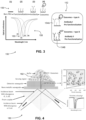
- FIG. 3 is a schematic illustration showing the functionalization of an active sensing layer, generally referenced 150, constructed and operative in accordance with a further embodiment of the disclosed technique.
- a target is to concentrate the EVs and exosomes subject for detection on the interface of the active sensing element (as shown in Figure 2 ) where the optical field intensity is largest. Since exosomes in general are characterized by protein-cargo on their membranes and inside the vesicles, a binding process of the exosomes in a microfluid sample can be executed using an appropriate antibody functionalization.
- a section 156 shows the various steps how an active sensing layer can be functionalized to a specific EV, for example a specific exosome.
- a section 152 shows how many sensing regions with different antibodies can be included in the active sensing layer to detect more than one target exosome.
- a section 154A shows antibodies for a first kind of exosome
- a section 154B shows antibodies for a second kind of exosome.
- PWCR plasmon-waveguide coupled resonance
- the hybrid modes of PWCR are coupled with pure highly sensitive plasmon modes to guided optical modes with high resolution.
- the outcome of this hybridization is plasmon-waveguide coupled (herein abbreviated PWC) modes with very high sensitivity and FOM.
- PWC plasmon-waveguide coupled
- the optical reflectance as a function of wavelength changes depending on what is adsorbed on the surface of the bare film. These differences can be used to detect and recognize the presence of an exosome.
- different types of exosomes will have varying amounts of optical reflectance.
- a shown dip 160 in the reflection modes represents the existence of a leaky-guided mode on the interface between the upper interface of the active sensing layer and the sensing region which is the space just above the upper interface.
- Shifts in the resonance wavelength reflect change in the local density near the upper interface thereby correlating with the accumulation rates on the upper surface of the interface. Consequently, according to the disclosed technique, changes in the resonance wavelength can be used to quantify the variations in the exosome concentrations in the sensed region.
- extracted bodily fluid from a patient is injected through a suitable microfluidic cavity (i.e., the inlet) that is attached on top of a sensing head (not labeled).
- the active region (active sensing layer 124) is composed of multiple layers in order to excite the required optical modes at the upper interface.
- the sensitivity of the optical modes to variations on the upper interface depends on the spectral region and the physical features of the EV structure. This sensitivity can be probed, as mentioned, using a broadband light source in the NIR region where the spectral signature of the reflected light correlates with the material adsorbed on the upper interface. These modes are very sensitive to small variation in the medium close to the interface.
- the optical reflectance will substantially change and can be recorded via reflected beam 134 on a spectrometer (not shown) in the output optical path.
- a spectrometer not shown
- multiple regions on the upper surface of the active region are functionalized with different antibodies and thus more than one EV target can be simultaneously detected according to the disclosed technique.
- Incident beam of light 130 emerges from a broadband source (not shown) that covers the working spectral region.
- the broadband source can be a white light source with low intensity thereby not deteriorating the tested sample of microfluid and not limiting the user.
- the detection mechanism is based on a weak probing of the reflected beam spectrum. As shown in graph 158 ( Figure 3 ), a distinct dip in the spectrum is obtained for the bare structure, reflecting the excitation of an optical guided mode in the dielectric waveguide. The successive adsorption of the antibody and the target EV entities subject for sensing will shift the dip, which can be detected by a standard spectrophotometer.
- the configuration of the disclosed technique does not make use of functionalized magnetic beads, electrochemical schemes, optical coherence tomography two photon luminescence or conventional fluorescence techniques for the detection of exosomes.
- the detection scheme of the disclosed technique as described above relates to surface plasmon waves and surface plasmon resonance and does not relate to surface enhanced Raman scattering (herein abbreviated SERS).
- SERS surface enhanced Raman scattering
- the disclosed technique does not make use of nanoparticle arrays nor functionalized nanoparticles with supramolecular sequences for the detection of biomarkers.
- nanoparticle arrays are substrates that require sophisticated fabrication techniques such as focused ion beam (herein abbreviated FIB) systems or electron beam lithography means.
- the active sensing element of the disclosed technique is composed of a number of two-dimensional (herein abbreviated 2D) layers not requiring any patterning.
- the metal layer in the active sensing element is very thin and can be prepared by sputtering with high quality which is a process that takes a number of minutes to fabricate.
- the disclosed technique provides for a cost effective EV detector which is inexpensive to fabricate and operate.
- Prior art systems for detecting EVs which use nanoparticle arrays e.g., hole-arrays
- Such detection requires the use of a cooled CCD spectrometer.
- Such systems are expensive and also need to be cooled to suppress or lower any possible thermal noise during use, which can be significant when the optical signal is very weak.
- reflectivity of an incident beam of light is measured from a 2D active sensing element thereby leading to a signal that is averaged over an entire area of a sensed region.
- a regular spectrometer in the visible or NIR regions, or in the EM spectrum, which significantly simplifies the measuring system as compared to a cooled CCD spectrometer.
- an SPR sensor having increased sensitivity by at least one to two orders of magnitude thereby enabling the detection of EVs such as microvesicles and exosomes.
- the increased sensitivity is achieved according to a coupling between a thin metal layer combined with a dielectric layer made from a polymer. This was shown above in Figure 1 .
- Both the thin metal layer and the dielectric layer have waveguides for generating optical guided modes from the incident light onto an analyte (i.e., a microfluid sample containing EVs) and receiving a reflection.
- the mode that is used for sensing the analyte is the guided mode inside the dielectric waveguides.
- SPW is only used to facilitate the excitation of the guided modes and to enable control of their sensitivity on the analyte.
- the disclosed technique has been described as a system and method for measuring changes in wavelength based on differences in reflectance which comes about through surface plasmon resonance coupled to highly-sensitive optical guided modes.
- the disclosed technique can also be embodied via a system and method for measuring changes in intensity as an indication of the presence of an exosome.
- the sensitivity of the system of the disclosed technique can be embodied as a measure of minute changes in intensity of the analyte (i.e., the microfluid sample containing the EVs).
- intensity of the reflected beam is the measured quantity for detecting the presence of specific exosomes and EVs.
- the light source would be a coherent light source in the very NIR region, for example a laser diode having an operational wavelength of 785 nanometers.
- the light source could also operate at other wavelengths according to the required sensitivity and detection dynamic range. This embodiment is explained in greater detail below in reference to Figure 7 .
- FIG. 4 is a schematic illustration of another EV detection system, generally referenced 180, constructed and operative in accordance with another embodiment of the disclosed technique.
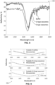
- EV detection system 180 is similar to EV detection system 120 ( Figure 2 ) however the detection system in Figure 4 shows the sensing region, delineated by a dotted line 182, wherein reflectance from resonance with exosomes in the sensing region can be detected.
- the penetration depth of the electromagnetic intensity inside the sensing medium determines the sensing range.
- the penetration depth of the field as shown in Figure 4 is on the order of 2 microns, thus in the example of the system shown, about 2% of the exosomes per unit area interacts with the incident beam of light.
- the percent weight of the exosomes in the buffer is about 10 -4 .
- the lowest detection limit of EV detection system 180 can be estimated as reaching 1.6 ⁇ 10 -5 percent weight.
- FIG. 5 is a graph showing a shift in the spectral profile of TE-polarized guided modes due to exosomes of types U and S, generally referenced 200, constructed and operative in accordance with a further embodiment of the disclosed technique.
- Graph 200 shows the reflectivity spectrum of U (i.e., urine-derive exosomes) and S (i.e., serum-derived exosomes) with respect to a reference measure only from the buffer medium. The shallow and broad dips originate from an incidence angle divergence effect.
- U i.e., urine-derive exosomes
- S i.e., serum-derived exosomes
- a distinct shift in the spectral profile of the TE-polarized guided modes due to exosomes of types U and S is clearly visible and achieved using the EV detection system of the disclosed technique. It is noted that in this embodiment, the presence of exosomes in a bulk medium can be detected without any functionalization of the sensing element with antibodies (as opposed to what was shown
- Figure 6 is a set of graphs showing reflectivity of the TE-polarized guided modes of Figure 5 in the vicinity of the resonance region fitted to a second-order polynomial profile, generally referenced 220, constructed and operative in accordance with another embodiment of the disclosed technique.
- the resonance wavelength of the reference buffer, U-type exosomes and S-type exosomes were 1489 nanometers, 1508 nanometers and 1501.3 nanometers respectively. These resonance wavelengths yield shifts of 19 nanometers for U-type exosomes and 12.9 nanometers for S-type exosomes.
- coupled plasmon-waveguide optical modes can be used to detect exosomes with a sensitivity of at least 10 -4 percent weight in a bulk medium, which is at least one order of magnitude higher in sensitivity than the sensitivity reported by the prior art.
- the EV detection system of the disclosed technique can not only detect the presence of exosomes with high sensitivity but can also distinguish between different exosomes from different sources.
- the disclosed technique can be used to detect exosomes and other EVs as biomarkers to detect the presence of cancers and other diseases of the body that exhibit a specific and unique exosome and/or EV signature.
- FIG. 7 is a schematic illustration showing the functionalization of an active sensing layer using an angular interrogation mode, generally referenced 240, constructed and operative in accordance with a further embodiment of the disclosed technique.
- a section 242 shows the functionalization steps as described above in section 156 ( Figure 3 ).
- a graph 244 shows the optical response along the functionalization process showing the shift in the resonance angle upon the adsorption of exosomes. This is illustrated on a line 246.
- the presence of exosomes is sensed by using an optical detector positioned at a fixed angle to the EV detection system (not shown) which tracks changes in the intensity of the reflected light.
- the optical detector may have a fixed angle in relation to the coupler (not shown) of the EV detection system.
- the numbers on the curves in graph 244 represent the optical intensity that is acquired at each of the functionalization steps.
- the calibration of the reflected intensity as a function of the coupling of the target exosomes sets the sensing mechanism.
- the incident wavelength is fixed and the reflectivity of the incident light versus the incident angle is scanned and measured.
- the detector is fixed at a given angle and detection is achieved according to intensity changes as a function of adsorption of the analyte.
- the observation plane represents the angle at which the detector is set and can be optimized for maximum sensitivity.
Landscapes
- Physics & Mathematics (AREA)
- Health & Medical Sciences (AREA)
- Chemical & Material Sciences (AREA)
- General Physics & Mathematics (AREA)
- Immunology (AREA)
- Life Sciences & Earth Sciences (AREA)
- Analytical Chemistry (AREA)
- Biochemistry (AREA)
- General Health & Medical Sciences (AREA)
- Pathology (AREA)
- Engineering & Computer Science (AREA)
- Optics & Photonics (AREA)
- Nuclear Medicine, Radiotherapy & Molecular Imaging (AREA)
- Microelectronics & Electronic Packaging (AREA)
- Nanotechnology (AREA)
- Investigating Or Analysing Materials By Optical Means (AREA)
Claims (11)
- Detektionssystem zum Detektieren mindestens eines extrazellulären Vesikels in einem Mikrofluid (122), umfassend:eine Breitbandlichtquelle, die mindestens einen einfallenden Lichtstrahl (130) im Bereich nahen Infrarots (NIR) erzeugt;Kollimationsoptik (128);Fokussieroptik (132);einen Koppler;ein Spektralphotometer; undein aktives Sensorelement (124), umfassend:ein Substrat (106);eine Metallschicht mit einer Stärke von 15-50 Nanometern, die auf dem Substrat (106) abgeschieden ist; undeine dielektrische Wellenleiterschicht (102), die auf der dünnen Metallschicht abgeschieden ist, wobei die dünne Metallschicht und die dielektrische Wellenleiterschicht (102) einen Wellenleiter umfassen;wobei die Kollimationsoptik (132) den Lichtstrahl (130) kollimiert, der über den Koppler mit dem Substrat gekoppelt ist; wobei die Fokussierungsoptik (132) über den Koppler mindestens eine Reflexion des mindestens einen einfallenden Lichtstrahls (130) von dem Substrat empfängt und die mindestens eine Reflexion an das Spektrophotometer bereitstellt;wobei das aktive Sensorelement (124) Oberflächenplasmonwellen in dem Mikrofluid (122) verursacht, wenn das Mikrofluid (122) in die Mikrofluidvorrichtung injiziert wird; undwobei das Spektrophotometer Resonanzwellenlängenverschiebungen in der mindestens einen Reflexion gemäß den Oberflächenplasmonwellen erfasst, wodurch das Vorhandensein des mindestens einen extrazellulären Vesikels in dem Mikrofluid (122) detektiert wird;wobei das Detektionssystem dadurch gekennzeichnet ist, dass es ferner eine mikrofluidische Vorrichtung umfasst, umfassend einen Einlass und einen Auslass, wobei das aktive Sensorelement (124) innerhalb der mikrofluidischen Vorrichtung angeordnet ist, und dass die dielektrische Wellenleiterschicht (102) eine polymere dielektrische Wellenleiterschicht mit einer Stärke zwischen 500-1500 Nanometern ist.
- Detektionssystem nach Anspruch 1, wobei der Koppler ausgewählt ist aus der Liste, bestehend aus:einem Prismenkoppler (126), der einen hohen Brechungsindex aufweist; undeinem Beugungsgitter.
- Detektionssystem nach Anspruch 1 oder 2, wobei das Spektralphotometer die mindestens eine Reflexion in einem Wellenlängenspektrum detektieren kann, das ausgewählt ist aus der Liste, bestehend aus:dem sichtbaren Wellenlängenspektrum;Spektrum für Nahinfrarot (NIR); unddem elektromagnetischen (EM) Spektrum.
- Detektionssystem nach einem der Ansprüche 1 bis 3, wobei die dünne Metallschicht ermöglicht, dass Energie des mindestens einen einfallenden Lichtstrahls (130) in den Wellenleiter getunnelt wird.
- Detektionssystem nach einem der Ansprüche 1 bis 4, wobei die Vielzahl von Wellenleitern eine Plasmonwellenleiterstruktur aufweisen.
- Detektionssystem nach einem der Ansprüche 1 bis 5, wobei die dünne Metallschicht und das Mikrofluid (122) in der mikrofluidischen Vorrichtung eine asymmetrische Umgebung für die Vielzahl von Wellenleitern erzeugen, wodurch eine Empfindlichkeit des aktiven Sensorelements erhöht wird.
- Detektionssystem nach einem der Ansprüche 1 bis 6, wobei eine obere Oberfläche des aktiven Sensorelements mit mindestens einem Antikörper funktionalisiert ist.
- Verfahren zum Herstellen des Detektionssystems nach einem der Ansprüche 1 bis 7 zum Detektieren mindestens eines extrazellulären Vesikels in einem Mikrofluid (122), wobei das aktive Sensorelement (124) hergestellt wird durch:Reinigen des Substrats (106), das ein Glassubstrat (106) ist;Abscheiden der dünnen Metallschicht auf dem Glassubstrat (106);Auflösen eines Polymers in einem geeigneten Lösungsmittel, um eine Polymerlösung zum Herstellen der dielektrischen Wellenleiterschicht (102) zu bilden;Aufbringen der Polymerlösung auf die Oberseite der dünnen Metallschicht; undGlühen des aktiven Sensorelements (124), wodurch die dielektrische Wellenleiterschicht (102) chemisch stabilisiert wird.
- Verfahren nach Anspruch 8, der Vorgang eines Auflösens umfassend den Teilvorgang eines Einstellens einer Stärke der dielektrischen Wellenleiterschicht (102) durch Modifizieren einer Viskosität der Polymerlösung.
- Verfahren nach Anspruch 8 oder 9, der Vorgang eines Aufbringens umfassend den Teilvorgang eines Feineinstellens einer Stärke der dielektrischen Wellenleiterschicht (102) unter Verwendung einer Spin-Coating-Technik.
- Verfahren nach einem der Ansprüche 8 bis 10, wobei der Vorgang eines Glühens unter Verwendung eines Ofens mit einer Temperatur in einem Bereich von 100-120 Grad Celsius ausgeführt wird.
Applications Claiming Priority (2)
| Application Number | Priority Date | Filing Date | Title |
|---|---|---|---|
| US201862696391P | 2018-07-11 | 2018-07-11 | |
| PCT/IL2019/050778 WO2020012482A1 (en) | 2018-07-11 | 2019-07-11 | Method and device for detecting extracellular vesicles |
Publications (3)
| Publication Number | Publication Date |
|---|---|
| EP3821232A1 EP3821232A1 (de) | 2021-05-19 |
| EP3821232A4 EP3821232A4 (de) | 2022-07-06 |
| EP3821232B1 true EP3821232B1 (de) | 2024-09-11 |
Family
ID=69141679
Family Applications (1)
| Application Number | Title | Priority Date | Filing Date |
|---|---|---|---|
| EP19833944.2A Active EP3821232B1 (de) | 2018-07-11 | 2019-07-11 | Verfahren und vorrichtung zur detektion von extrazellulären vesikeln |
Country Status (4)
| Country | Link |
|---|---|
| US (2) | US11513074B2 (de) |
| EP (1) | EP3821232B1 (de) |
| IL (1) | IL279961B2 (de) |
| WO (1) | WO2020012482A1 (de) |
Families Citing this family (2)
| Publication number | Priority date | Publication date | Assignee | Title |
|---|---|---|---|---|
| US11639895B2 (en) * | 2021-03-09 | 2023-05-02 | Globalfoundries U.S. Inc. | Device including optofluidic sensor with integrated photodiode |
| CN121633059B (zh) * | 2026-02-04 | 2026-04-07 | 中国科学院长春光学精密机械与物理研究所 | 基于sers基底的光流控拉曼传感芯片及其制备方法 |
Family Cites Families (30)
| Publication number | Priority date | Publication date | Assignee | Title |
|---|---|---|---|---|
| CA1321488C (en) * | 1987-08-22 | 1993-08-24 | Martin Francis Finlan | Biological sensors |
| SE462408B (sv) | 1988-11-10 | 1990-06-18 | Pharmacia Ab | Optiskt biosensorsystem utnyttjande ytplasmonresonans foer detektering av en specific biomolekyl, saett att kalibrera sensoranordningen samt saett att korrigera foer baslinjedrift i systemet |
| US5485277A (en) | 1994-07-26 | 1996-01-16 | Physical Optics Corporation | Surface plasmon resonance sensor and methods for the utilization thereof |
| DE59912658D1 (de) * | 1998-11-20 | 2005-11-17 | Graffinity Pharmaceuticals Ag | Messanordnung und messmethode zum parallelen auslesen von spr-sensoren |
| US7177515B2 (en) * | 2002-03-20 | 2007-02-13 | The Regents Of The University Of Colorado | Surface plasmon devices |
| KR101168654B1 (ko) | 2004-05-19 | 2012-07-25 | 브이피 호울딩 엘엘씨 | 표면 증강 라만 산란에 의한 화학기의 증강된 검출을 위한 층상의 플라즈몬 구조를 가진 광센서 |
| TWI247886B (en) * | 2005-01-06 | 2006-01-21 | Univ Nat Taiwan | Improved linear wave-guide type surface plasmon resonance micro sensor |
| US8355136B2 (en) * | 2005-12-16 | 2013-01-15 | Indiana University Research And Technology Corporation | Sub-micron surface plasmon resonance sensor systems |
| AU2006329841A1 (en) | 2005-12-16 | 2007-07-05 | Indiana University Research & Technology Corporation | Sub-micron surface plasmon resonance sensor systems |
| US20090097022A1 (en) | 2007-08-24 | 2009-04-16 | Dynamic Throughput Inc. | Discovery tool with integrated microfluidic biomarker optical detection array device and methods for use |
| WO2009030071A1 (en) * | 2007-09-06 | 2009-03-12 | National Center For Nanoscience And Technology, China | Wave-guide coupling spr sensor chip and sensor chip array thereof |
| US20110188043A1 (en) | 2007-12-26 | 2011-08-04 | Yissum, Research Development Company of The Hebrew University of Jerusalem, Ltd. | Method and apparatus for monitoring processes in living cells |
| JP5180703B2 (ja) * | 2008-06-27 | 2013-04-10 | 富士フイルム株式会社 | 検出方法、検出用試料セルおよび検出用キット |
| JP5621983B2 (ja) * | 2008-09-01 | 2014-11-12 | 日立化成株式会社 | Sprセンサー |
| WO2010091293A1 (en) | 2009-02-06 | 2010-08-12 | The Regents Of The University Of California | Plasmonic system for detecting binding of biological molecules |
| US20140170024A1 (en) * | 2011-07-15 | 2014-06-19 | National Institute Of Advanced Industrial Science And Technology | Target substance detection chip, target substance detection plate, target substance detection device and target substance detection method |
| JP2013061301A (ja) * | 2011-09-15 | 2013-04-04 | Nitto Denko Corp | Sprセンサセルおよびsprセンサ |
| JP2013181753A (ja) * | 2012-02-29 | 2013-09-12 | Nitto Denko Corp | Sprセンサセルおよびsprセンサ |
| JP5946330B2 (ja) * | 2012-06-01 | 2016-07-06 | 日東電工株式会社 | Sprセンサセルおよびsprセンサ |
| US20140094383A1 (en) | 2012-10-02 | 2014-04-03 | Ohio State Innovation Foundation | Tethered Lipoplex nanoparticle Biochips And Methods Of Use |
| US9482513B2 (en) | 2013-03-14 | 2016-11-01 | Research Development Foundation | Apparatus and methods for optical coherence tomography and two-photon luminescence imaging |
| EP3028033B1 (de) * | 2013-08-04 | 2020-10-07 | Photonicsys Ltd. | Optischer sensor auf der basis einer mehrschichtigen plasmonischen struktur mit nanoporöser metallschicht |
| WO2015084800A1 (en) | 2013-12-02 | 2015-06-11 | The General Hospital Corporation | Nano-plasmonic sensor for exosome detection |
| WO2015168776A1 (en) * | 2014-05-08 | 2015-11-12 | The Governing Council Of The University Of Toronto | Multimode spectroscopy apparatuses and methods |
| KR101758428B1 (ko) | 2014-06-02 | 2017-07-18 | 인천대학교 산학협력단 | 분자 비컨을 이용한 엑소좀 miRNA의 검출 방법 |
| JP2016038395A (ja) * | 2014-08-05 | 2016-03-22 | 日東電工株式会社 | 光導波路への光の入射方法 |
| US10801956B2 (en) * | 2015-08-26 | 2020-10-13 | Photonicsys Ltd. | Resonant periodic structures and methods of using them as filters and sensors |
| WO2017165800A2 (en) | 2016-03-25 | 2017-09-28 | The Board Of Regents Of The University Of Texas System | Nanosensors and methods for detection of biological markers |
| CN105974122B (zh) | 2016-05-04 | 2018-09-28 | 华东医药(杭州)基因科技有限公司 | 一种检测外泌体gpc1蛋白的方法 |
| US10254216B2 (en) | 2016-06-30 | 2019-04-09 | Schlumberger Technology Corporation | Systems, methods and apparatus for analysis of reservoir fluids using surface plasmon resonance |
-
2019
- 2019-07-11 EP EP19833944.2A patent/EP3821232B1/de active Active
- 2019-07-11 IL IL279961A patent/IL279961B2/en unknown
- 2019-07-11 WO PCT/IL2019/050778 patent/WO2020012482A1/en not_active Ceased
- 2019-07-11 US US17/257,451 patent/US11513074B2/en active Active
-
2022
- 2022-10-18 US US17/968,456 patent/US20230043792A1/en not_active Abandoned
Also Published As
| Publication number | Publication date |
|---|---|
| IL279961B1 (en) | 2024-11-01 |
| EP3821232A4 (de) | 2022-07-06 |
| IL279961A (en) | 2021-03-01 |
| US20230043792A1 (en) | 2023-02-09 |
| WO2020012482A1 (en) | 2020-01-16 |
| US11513074B2 (en) | 2022-11-29 |
| US20210293703A1 (en) | 2021-09-23 |
| IL279961B2 (en) | 2025-03-01 |
| EP3821232A1 (de) | 2021-05-19 |
Similar Documents
| Publication | Publication Date | Title |
|---|---|---|
| Konopsky et al. | Photonic crystal surface waves for optical biosensors | |
| Ricciardi et al. | Lab-on-fiber technology: a new vision for chemical and biological sensing | |
| Haider et al. | Multi-analyte detection based on integrated internal and external sensing approach | |
| Chen et al. | Review of surface plasmon resonance and localized surface plasmon resonance sensor | |
| TWI364533B (en) | A method for improving surface plasmon resonance by using conducting metal oxide as adhesive layer | |
| US7271914B2 (en) | Biomolecular sensor system utilizing a transverse propagation wave of surface plasmon resonance (SPR) | |
| Sreekanth et al. | Hyperbolic metamaterials-based plasmonic biosensor for fluid biopsy with single molecule sensitivity | |
| EP3524351A1 (de) | Biomarker-erfassungsvorrichtung | |
| US20230043792A1 (en) | Method and device for detecting extracellular vesicles | |
| US12078595B2 (en) | Nanoplasmonic devices and applications thereof | |
| Jian et al. | Enhancement of the volume refractive index sensing by ROTE and its application on cancer and normal cells discrimination | |
| Zhao et al. | Extreme sensitivity biosensing platform based on Fano resonance and graphene oxide | |
| CN117470777A (zh) | 光学传感器、检测方法及用途 | |
| Esinesco et al. | SU-8 micro-biosensor based on Mach-Zehnder interferometer | |
| Jha et al. | Design of a silicon-based plasmonic biosensor chip for human blood-group identification | |
| Thawany et al. | Detection of circulating tumor cells using D-optical fiber SPR sensor | |
| Liu et al. | Optical integrated chips with micro and nanostructures for refractive index and SERS‐based optical label‐free sensing | |
| Yasar et al. | Advancement in Breast Cancer Diagnosis: Detecting CA15-3 Antigen Using Surface Plasmon Resonance in Photonic Crystal Fiber | |
| Beffara | SERS biosensors based on special optical fibers for clinical diagnosis | |
| WO2019049817A1 (ja) | センサチップ、目的物質検出装置及び目的物質検出方法 | |
| Konopsky et al. | Optical biosensors based on photonic crystal surface waves | |
| Perotto | On chip optical sensing | |
| Chatzianagnostou | Design and Optimization of Integrated Plasmo-photonic Sensors | |
| Bode et al. | Multilayer Plasmonic Biosensor with Enhanced Evanescent Field Confinement for Early Detection of Blood Cancer | |
| Othman | Methods for Infrared Spectral Sensing of Chemical and Biological Matter at the Microscale: Theory and Experiments |
Legal Events
| Date | Code | Title | Description |
|---|---|---|---|
| STAA | Information on the status of an ep patent application or granted ep patent |
Free format text: STATUS: THE INTERNATIONAL PUBLICATION HAS BEEN MADE |
|
| PUAI | Public reference made under article 153(3) epc to a published international application that has entered the european phase |
Free format text: ORIGINAL CODE: 0009012 |
|
| STAA | Information on the status of an ep patent application or granted ep patent |
Free format text: STATUS: REQUEST FOR EXAMINATION WAS MADE |
|
| 17P | Request for examination filed |
Effective date: 20210129 |
|
| AK | Designated contracting states |
Kind code of ref document: A1 Designated state(s): AL AT BE BG CH CY CZ DE DK EE ES FI FR GB GR HR HU IE IS IT LI LT LU LV MC MK MT NL NO PL PT RO RS SE SI SK SM TR |
|
| DAV | Request for validation of the european patent (deleted) | ||
| DAX | Request for extension of the european patent (deleted) | ||
| RIC1 | Information provided on ipc code assigned before grant |
Ipc: G02B 6/122 20060101ALI20220208BHEP Ipc: G01N 21/64 20060101ALI20220208BHEP Ipc: G01N 29/24 20060101ALI20220208BHEP Ipc: G01N 29/02 20060101ALI20220208BHEP Ipc: G01N 21/552 20140101AFI20220208BHEP |
|
| A4 | Supplementary search report drawn up and despatched |
Effective date: 20220608 |
|
| RIC1 | Information provided on ipc code assigned before grant |
Ipc: G02B 6/122 20060101ALI20220601BHEP Ipc: G01N 21/64 20060101ALI20220601BHEP Ipc: G01N 29/24 20060101ALI20220601BHEP Ipc: G01N 29/02 20060101ALI20220601BHEP Ipc: G01N 21/552 20140101AFI20220601BHEP |
|
| STAA | Information on the status of an ep patent application or granted ep patent |
Free format text: STATUS: EXAMINATION IS IN PROGRESS |
|
| 17Q | First examination report despatched |
Effective date: 20230717 |
|
| GRAP | Despatch of communication of intention to grant a patent |
Free format text: ORIGINAL CODE: EPIDOSNIGR1 |
|
| STAA | Information on the status of an ep patent application or granted ep patent |
Free format text: STATUS: GRANT OF PATENT IS INTENDED |
|
| INTG | Intention to grant announced |
Effective date: 20240426 |
|
| GRAS | Grant fee paid |
Free format text: ORIGINAL CODE: EPIDOSNIGR3 |
|
| GRAA | (expected) grant |
Free format text: ORIGINAL CODE: 0009210 |
|
| STAA | Information on the status of an ep patent application or granted ep patent |
Free format text: STATUS: THE PATENT HAS BEEN GRANTED |
|
| AK | Designated contracting states |
Kind code of ref document: B1 Designated state(s): AL AT BE BG CH CY CZ DE DK EE ES FI FR GB GR HR HU IE IS IT LI LT LU LV MC MK MT NL NO PL PT RO RS SE SI SK SM TR |
|
| REG | Reference to a national code |
Ref country code: GB Ref legal event code: FG4D |
|
| REG | Reference to a national code |
Ref country code: CH Ref legal event code: EP |
|
| P01 | Opt-out of the competence of the unified patent court (upc) registered |
Free format text: CASE NUMBER: APP_46264/2024 Effective date: 20240809 |
|
| REG | Reference to a national code |
Ref country code: DE Ref legal event code: R096 Ref document number: 602019058834 Country of ref document: DE |
|
| REG | Reference to a national code |
Ref country code: IE Ref legal event code: FG4D |
|
| REG | Reference to a national code |
Ref country code: LT Ref legal event code: MG9D |
|
| PG25 | Lapsed in a contracting state [announced via postgrant information from national office to epo] |
Ref country code: NO Free format text: LAPSE BECAUSE OF FAILURE TO SUBMIT A TRANSLATION OF THE DESCRIPTION OR TO PAY THE FEE WITHIN THE PRESCRIBED TIME-LIMIT Effective date: 20241211 |
|
| REG | Reference to a national code |
Ref country code: NL Ref legal event code: MP Effective date: 20240911 |
|
| PG25 | Lapsed in a contracting state [announced via postgrant information from national office to epo] |
Ref country code: GR Free format text: LAPSE BECAUSE OF FAILURE TO SUBMIT A TRANSLATION OF THE DESCRIPTION OR TO PAY THE FEE WITHIN THE PRESCRIBED TIME-LIMIT Effective date: 20241212 Ref country code: FI Free format text: LAPSE BECAUSE OF FAILURE TO SUBMIT A TRANSLATION OF THE DESCRIPTION OR TO PAY THE FEE WITHIN THE PRESCRIBED TIME-LIMIT Effective date: 20240911 |
|
| PG25 | Lapsed in a contracting state [announced via postgrant information from national office to epo] |
Ref country code: BG Free format text: LAPSE BECAUSE OF FAILURE TO SUBMIT A TRANSLATION OF THE DESCRIPTION OR TO PAY THE FEE WITHIN THE PRESCRIBED TIME-LIMIT Effective date: 20240911 |
|
| PG25 | Lapsed in a contracting state [announced via postgrant information from national office to epo] |
Ref country code: LV Free format text: LAPSE BECAUSE OF FAILURE TO SUBMIT A TRANSLATION OF THE DESCRIPTION OR TO PAY THE FEE WITHIN THE PRESCRIBED TIME-LIMIT Effective date: 20240911 |
|
| PG25 | Lapsed in a contracting state [announced via postgrant information from national office to epo] |
Ref country code: HR Free format text: LAPSE BECAUSE OF FAILURE TO SUBMIT A TRANSLATION OF THE DESCRIPTION OR TO PAY THE FEE WITHIN THE PRESCRIBED TIME-LIMIT Effective date: 20240911 |
|
| PG25 | Lapsed in a contracting state [announced via postgrant information from national office to epo] |
Ref country code: RS Free format text: LAPSE BECAUSE OF FAILURE TO SUBMIT A TRANSLATION OF THE DESCRIPTION OR TO PAY THE FEE WITHIN THE PRESCRIBED TIME-LIMIT Effective date: 20241211 Ref country code: ES Free format text: LAPSE BECAUSE OF FAILURE TO SUBMIT A TRANSLATION OF THE DESCRIPTION OR TO PAY THE FEE WITHIN THE PRESCRIBED TIME-LIMIT Effective date: 20240911 |
|
| PG25 | Lapsed in a contracting state [announced via postgrant information from national office to epo] |
Ref country code: RS Free format text: LAPSE BECAUSE OF FAILURE TO SUBMIT A TRANSLATION OF THE DESCRIPTION OR TO PAY THE FEE WITHIN THE PRESCRIBED TIME-LIMIT Effective date: 20241211 Ref country code: NO Free format text: LAPSE BECAUSE OF FAILURE TO SUBMIT A TRANSLATION OF THE DESCRIPTION OR TO PAY THE FEE WITHIN THE PRESCRIBED TIME-LIMIT Effective date: 20241211 Ref country code: LV Free format text: LAPSE BECAUSE OF FAILURE TO SUBMIT A TRANSLATION OF THE DESCRIPTION OR TO PAY THE FEE WITHIN THE PRESCRIBED TIME-LIMIT Effective date: 20240911 Ref country code: HR Free format text: LAPSE BECAUSE OF FAILURE TO SUBMIT A TRANSLATION OF THE DESCRIPTION OR TO PAY THE FEE WITHIN THE PRESCRIBED TIME-LIMIT Effective date: 20240911 Ref country code: GR Free format text: LAPSE BECAUSE OF FAILURE TO SUBMIT A TRANSLATION OF THE DESCRIPTION OR TO PAY THE FEE WITHIN THE PRESCRIBED TIME-LIMIT Effective date: 20241212 Ref country code: FI Free format text: LAPSE BECAUSE OF FAILURE TO SUBMIT A TRANSLATION OF THE DESCRIPTION OR TO PAY THE FEE WITHIN THE PRESCRIBED TIME-LIMIT Effective date: 20240911 Ref country code: ES Free format text: LAPSE BECAUSE OF FAILURE TO SUBMIT A TRANSLATION OF THE DESCRIPTION OR TO PAY THE FEE WITHIN THE PRESCRIBED TIME-LIMIT Effective date: 20240911 Ref country code: BG Free format text: LAPSE BECAUSE OF FAILURE TO SUBMIT A TRANSLATION OF THE DESCRIPTION OR TO PAY THE FEE WITHIN THE PRESCRIBED TIME-LIMIT Effective date: 20240911 |
|
| REG | Reference to a national code |
Ref country code: AT Ref legal event code: MK05 Ref document number: 1723107 Country of ref document: AT Kind code of ref document: T Effective date: 20240911 |
|
| PG25 | Lapsed in a contracting state [announced via postgrant information from national office to epo] |
Ref country code: NL Free format text: LAPSE BECAUSE OF FAILURE TO SUBMIT A TRANSLATION OF THE DESCRIPTION OR TO PAY THE FEE WITHIN THE PRESCRIBED TIME-LIMIT Effective date: 20240911 |
|
| PG25 | Lapsed in a contracting state [announced via postgrant information from national office to epo] |
Ref country code: IS Free format text: LAPSE BECAUSE OF FAILURE TO SUBMIT A TRANSLATION OF THE DESCRIPTION OR TO PAY THE FEE WITHIN THE PRESCRIBED TIME-LIMIT Effective date: 20250111 Ref country code: PT Free format text: LAPSE BECAUSE OF FAILURE TO SUBMIT A TRANSLATION OF THE DESCRIPTION OR TO PAY THE FEE WITHIN THE PRESCRIBED TIME-LIMIT Effective date: 20250113 |
|
| PG25 | Lapsed in a contracting state [announced via postgrant information from national office to epo] |
Ref country code: RO Free format text: LAPSE BECAUSE OF FAILURE TO SUBMIT A TRANSLATION OF THE DESCRIPTION OR TO PAY THE FEE WITHIN THE PRESCRIBED TIME-LIMIT Effective date: 20240911 Ref country code: SM Free format text: LAPSE BECAUSE OF FAILURE TO SUBMIT A TRANSLATION OF THE DESCRIPTION OR TO PAY THE FEE WITHIN THE PRESCRIBED TIME-LIMIT Effective date: 20240911 |
|
| PG25 | Lapsed in a contracting state [announced via postgrant information from national office to epo] |
Ref country code: EE Free format text: LAPSE BECAUSE OF FAILURE TO SUBMIT A TRANSLATION OF THE DESCRIPTION OR TO PAY THE FEE WITHIN THE PRESCRIBED TIME-LIMIT Effective date: 20240911 Ref country code: AT Free format text: LAPSE BECAUSE OF FAILURE TO SUBMIT A TRANSLATION OF THE DESCRIPTION OR TO PAY THE FEE WITHIN THE PRESCRIBED TIME-LIMIT Effective date: 20240911 |
|
| PG25 | Lapsed in a contracting state [announced via postgrant information from national office to epo] |
Ref country code: CZ Free format text: LAPSE BECAUSE OF FAILURE TO SUBMIT A TRANSLATION OF THE DESCRIPTION OR TO PAY THE FEE WITHIN THE PRESCRIBED TIME-LIMIT Effective date: 20240911 Ref country code: PL Free format text: LAPSE BECAUSE OF FAILURE TO SUBMIT A TRANSLATION OF THE DESCRIPTION OR TO PAY THE FEE WITHIN THE PRESCRIBED TIME-LIMIT Effective date: 20240911 |
|
| PG25 | Lapsed in a contracting state [announced via postgrant information from national office to epo] |
Ref country code: SK Free format text: LAPSE BECAUSE OF FAILURE TO SUBMIT A TRANSLATION OF THE DESCRIPTION OR TO PAY THE FEE WITHIN THE PRESCRIBED TIME-LIMIT Effective date: 20240911 Ref country code: IT Free format text: LAPSE BECAUSE OF FAILURE TO SUBMIT A TRANSLATION OF THE DESCRIPTION OR TO PAY THE FEE WITHIN THE PRESCRIBED TIME-LIMIT Effective date: 20240911 |
|
| REG | Reference to a national code |
Ref country code: DE Ref legal event code: R097 Ref document number: 602019058834 Country of ref document: DE |
|
| PG25 | Lapsed in a contracting state [announced via postgrant information from national office to epo] |
Ref country code: DK Free format text: LAPSE BECAUSE OF FAILURE TO SUBMIT A TRANSLATION OF THE DESCRIPTION OR TO PAY THE FEE WITHIN THE PRESCRIBED TIME-LIMIT Effective date: 20240911 |
|
| PLBE | No opposition filed within time limit |
Free format text: ORIGINAL CODE: 0009261 |
|
| STAA | Information on the status of an ep patent application or granted ep patent |
Free format text: STATUS: NO OPPOSITION FILED WITHIN TIME LIMIT |
|
| 26N | No opposition filed |
Effective date: 20250612 |
|
| PG25 | Lapsed in a contracting state [announced via postgrant information from national office to epo] |
Ref country code: SE Free format text: LAPSE BECAUSE OF FAILURE TO SUBMIT A TRANSLATION OF THE DESCRIPTION OR TO PAY THE FEE WITHIN THE PRESCRIBED TIME-LIMIT Effective date: 20240911 |
|
| REG | Reference to a national code |
Ref country code: DE Ref legal event code: R119 Ref document number: 602019058834 Country of ref document: DE |
|
| REG | Reference to a national code |
Ref country code: CH Ref legal event code: H13 Free format text: ST27 STATUS EVENT CODE: U-0-0-H10-H13 (AS PROVIDED BY THE NATIONAL OFFICE) Effective date: 20260224 |
|
| PG25 | Lapsed in a contracting state [announced via postgrant information from national office to epo] |
Ref country code: LU Free format text: LAPSE BECAUSE OF NON-PAYMENT OF DUE FEES Effective date: 20250711 |
|
| GBPC | Gb: european patent ceased through non-payment of renewal fee |
Effective date: 20250711 |
|
| REG | Reference to a national code |
Ref country code: BE Ref legal event code: MM Effective date: 20250731 |
|
| PG25 | Lapsed in a contracting state [announced via postgrant information from national office to epo] |
Ref country code: GB Free format text: LAPSE BECAUSE OF NON-PAYMENT OF DUE FEES Effective date: 20250711 |
|
| PG25 | Lapsed in a contracting state [announced via postgrant information from national office to epo] |
Ref country code: DE Free format text: LAPSE BECAUSE OF NON-PAYMENT OF DUE FEES Effective date: 20260203 |
|
| PG25 | Lapsed in a contracting state [announced via postgrant information from national office to epo] |
Ref country code: BE Free format text: LAPSE BECAUSE OF NON-PAYMENT OF DUE FEES Effective date: 20250731 |
|
| PG25 | Lapsed in a contracting state [announced via postgrant information from national office to epo] |
Ref country code: FR Free format text: LAPSE BECAUSE OF NON-PAYMENT OF DUE FEES Effective date: 20250731 |