EP3821574B1 - Digitaler isolator - Google Patents
Digitaler isolator Download PDFInfo
- Publication number
- EP3821574B1 EP3821574B1 EP19736393.0A EP19736393A EP3821574B1 EP 3821574 B1 EP3821574 B1 EP 3821574B1 EP 19736393 A EP19736393 A EP 19736393A EP 3821574 B1 EP3821574 B1 EP 3821574B1
- Authority
- EP
- European Patent Office
- Prior art keywords
- equal
- signal
- node
- equals
- sawtooth
- Prior art date
- Legal status (The legal status is an assumption and is not a legal conclusion. Google has not performed a legal analysis and makes no representation as to the accuracy of the status listed.)
- Active
Links
Images



Classifications
-
- H—ELECTRICITY
- H04—ELECTRIC COMMUNICATION TECHNIQUE
- H04L—TRANSMISSION OF DIGITAL INFORMATION, e.g. TELEGRAPHIC COMMUNICATION
- H04L25/00—Baseband systems
- H04L25/02—Details ; arrangements for supplying electrical power along data transmission lines
- H04L25/0264—Arrangements for coupling to transmission lines
- H04L25/0266—Arrangements for providing Galvanic isolation, e.g. by means of magnetic or capacitive coupling
-
- G—PHYSICS
- G08—SIGNALLING
- G08C—TRANSMISSION SYSTEMS FOR MEASURED VALUES, CONTROL OR SIMILAR SIGNALS
- G08C19/00—Electric signal transmission systems
-
- H—ELECTRICITY
- H03—ELECTRONIC CIRCUITRY
- H03K—PULSE TECHNIQUE
- H03K19/00—Logic circuits, i.e. having at least two inputs acting on one output; Inverting circuits
- H03K19/0175—Coupling arrangements; Interface arrangements
- H03K19/0185—Coupling arrangements; Interface arrangements using field effect transistors only
- H03K19/018507—Interface arrangements
- H03K19/01855—Interface arrangements synchronous, i.e. using clock signals
-
- H—ELECTRICITY
- H04—ELECTRIC COMMUNICATION TECHNIQUE
- H04L—TRANSMISSION OF DIGITAL INFORMATION, e.g. TELEGRAPHIC COMMUNICATION
- H04L25/00—Baseband systems
- H04L25/02—Details ; arrangements for supplying electrical power along data transmission lines
- H04L25/0264—Arrangements for coupling to transmission lines
- H04L25/0272—Arrangements for coupling to multiple lines, e.g. for differential transmission
-
- H—ELECTRICITY
- H03—ELECTRONIC CIRCUITRY
- H03K—PULSE TECHNIQUE
- H03K4/00—Generating pulses having essentially a finite slope or stepped portions
- H03K4/06—Generating pulses having essentially a finite slope or stepped portions having triangular shape
- H03K4/08—Generating pulses having essentially a finite slope or stepped portions having triangular shape having sawtooth shape
- H03K4/48—Generating pulses having essentially a finite slope or stepped portions having triangular shape having sawtooth shape using as active elements semiconductor devices
- H03K4/50—Generating pulses having essentially a finite slope or stepped portions having triangular shape having sawtooth shape using as active elements semiconductor devices in which a sawtooth voltage is produced across a capacitor
Definitions
- the present invention generally relates to the field of capacitive isolation links.
- the invention relates to the field of capacitive isolation systems for use in isolating electrical circuits from one another while transmitting digital information data. More particularly, this invention relates to isolation systems having capacitor-coupled isolation barriers. This is useful in, for example, industrial process control application, telephony, medical electronics, data communication.
- Isolators are generally implemented to separate circuits or circuit sections of the electrical circuit to one another from undesired influence of, as for example but not limiting, other circuits or circuit sections, to minimize the influence of common mode transients (CMT), influence of radiation or electromagnetic interferences, cross talk, between circuits or circuit sections.
- CMT common mode transients
- Capacitive isolation links are also used to minimize the transmission of interferences introduced by the environment from one circuit to another or from one section of a circuit to one another. It is also used in galvanic isolation, to isolate high voltages from one another or to isolate low voltage command circuits to high voltage power circuits. Capacitive isolation links also allow better integration compared to other systems based for example on electromagnetic isolators.
- Capacitive isolation links usually make use of a dielectric in order to block direct current between isolated circuits sections of the electrical circuits or to block lowest-frequency currents between the circuits sections while allowing transfer of a higher frequency data signal.
- the isolation barrier usually includes one or more capacitors or transformers. For this reason, information data shape commonly used is square signals with very fast transients used for the edges of the signal followed by a maintained information level (no transient information) allowing to transmit only the edge variation of the signal through the capacitive barrier.
- CMT common mode transients
- a decision logic (DCL) at the driving output of the flip-flop measures the durations between signal transients. If the duration between two consecutive transients exceeds a certain time limit (as in the case of a low-frequency signal) the DCL forces the output-multiplexer to switch from the high-frequency to the low-frequency channel. Because low-frequency input signals require the internal capacitors to assume prohibitively large values, these signals are pulse-width modulated (PWM) with the carrier frequency of an internal oscillator, thus creating a sufficiently high frequency, capable of passing the capacitive barrier. As the input is modulated, a low-pass filter (LPF) is needed to remove the high-frequency carrier from the actual data before passing it on to the output multiplexer.
- PWM pulse-width modulated
- LPF low-pass filter
- Document US2017/0302225A1 discloses a system where the input circuit includes an on-off keying (OOK) modulator configured to generate a modulated data signal in response to the input data signal and the carrier signal.
- the output circuit includes a frequency shift keying (FSK) demodulator configured to detect a presence of the carrier signal in the modulated differential data signal and generate a demodulated data signal in response to the presence of the carrier signal.
- OOK on-off keying
- FSK frequency shift keying
- Patent EP0973305A1 discloses a capacitive insulating barrier system with a sawtooth signal as a carrier to generate a Pulse Width Modulation (PWM) signal as an input signal of the capacitive insulation barrier. There are two capacitors between input and output circuit which provide isolation between input and output circuits. A square pulse width modulated signal is used as transmitted signal from one side of the isolation barrier to the other.
- PWM Pulse Width Modulation
- US-6144326-B1 discloses digital isolation in a public telephony system.
- the analog input is sigma delta converted to a digital signal, modulated with a pulse density modulation and transmitted via capacitors in a differential mode through two lines.
- a clock is recovered from the differential signal, the signal decoded and converted to analog output.
- the modulated signal further needs to be demodulated. This adds delay and jitter. This can be critical or not, depending on the final application.
- a square or sinusoidal signal is applied at the input of a capacitive link.
- a specific demodulator is required, leading to some delay and jitter. It can also require some magnetics to generate such waveforms.
- the capacitor In case of square waves, the capacitor will always transmit a rising edge followed by a constant state and then by a falling edge.
- the capacitive link is a high pass filter.
- the invention is defined by the appended independent claims. Additional embodiments are defined by the dependent claims.
- the invention provides a digital isolator for receiving a digital signal D, with reference to a first ground G1, and providing corresponding signals to output node R and output node S with reference to a second ground G2.
- the digital isolator may comprise at least one logic module for receiving said digital signal D.
- Said at least one logic module may comprise a clock generator generating a clock signal CLK having a period T0 and, in a preferred embodiment, a pulse width shorter than T0/3.
- Said logic module is configured to provide first and second command signals to at least one sawtooth modulator.
- Said clock signal is used together with said input signal D to generate through said logic module, said logic commands to said sawtooth modulators.
- a first sawtooth modulator STM1 for receiving said first command signals is configured for providing a first sawtooth signal at a node A1, output of STM1.
- Said first sawtooth signal is composed of a fast rising edge triggered by a rising edge of the clock signal CLK, followed by a slow falling edge, when D equals 1 and is composed of a fast falling edge triggered by a rising edge of the clock signal CLK, followed by a slow rising edge, when D equals 0.
- a second sawtooth modulator STM2 is configured for receiving said second command signals, and for providing a second sawtooth signal at a node A2, output of STM2.
- Said second sawtooth signal is composed of a fast falling edge triggered by a rising edge of the clock signal CLK, followed by a slow rising edge, when D equals 1 and a fast rising edge triggered by a rising edge of the clock signal CLK, followed by a slow falling edge, when D equals 0 such that the two said sawtooth signals generated respectively by STM1 and STM2 provide data information of inversed logic.
- Said node A1 is the input node of a first isolation capacitor used for isolating the circuit sections of the system on a first channel of the differential circuit.
- B1 is the second node of the said first isolation capacitor.
- B1 is used as output of the first isolation capacitor for the said first channel of the differential link.
- the first isolation capacitor used as isolation barrier is also used as part of a high-pass filter together with dipole Z1.
- Z1 is connected between said node B1 and a bias voltage source with reference to a second ground G2.
- Said node A2 is the input node of a second isolation capacitor used for isolating the circuit sections of the system on the second channel of the said differential link.
- B2 is the second node of the said second isolation capacitor.
- B2 is used as output of the capacitive barrier for the second channel of the differential link.
- the second isolation capacitor used as isolation barrier is also used as part of a high-pass filter together with dipole Z2.
- Z2 is connected between said node B2 and said bias voltage source with reference to a second ground G2.
- a first threshold comparator having a first input connected to said node B1, and a second input connected to said node B2, produces a logical 1 output S when the difference between the value of its first input exceeds its second input by a threshold Th1, and logical 0 output otherwise.
- a second threshold comparator having a first input connected to said node B2, and a second input connected to said node B1, produce a logical 1 output R when its first input exceeds its second input by a threshold Th2, and a logical 0 output otherwise.
- the dipoles Z1, Z2 may be resistors.
- the bias voltage source may have a zero bias, i.e. be a short circuit.
- the durations of the slow rising edges and/or of the slow falling edges at said nodes A1 and/or A2 are at least two times, four times, or more preferably ten times the durations of the corresponding fast falling edges and/or fast rising edges, respectively.
- the duration of the slow or fast riding edges may be determined as being the time needed for reaching a ratio such as 80% of a power supply voltage.
- the duration of the slow or fast falling edges may be determined as being the time needed for falling down to a ratio such as 20% of a power supply voltage.
- said logic module may comprise means for disabling the clock generator at a transition of the digital signal D, and for re-enabling the clock generator after a delay larger than or equal to 0.8*T0 afterwards. This provides an anti-jitter solution.
- an additional digital signal D1 with reference to said first ground G1 may be used as input digital signal, said logic module comprising additional means for disabling the clock generator when additional digital signal D1 is equal to logical 0.
- Said input signal D, with reference to said first ground G1 may then be used as a selector for sending a signal corresponding signal to additional digital signal D1 on output R or output S, with reference to said second ground G2, depending on the logic value of said signal D.
- Signal D acts as a selector for sending signal D1 either to output S or output R.
- said logic module may be configured for providing first command signals to said first sawtooth modulator STM1, said first command signals comprising logical signals SU1, SD1 and W1.
- Said logic module may also be configured for providing second command signals to said second sawtooth modulator STM2, said second command signals comprising logical signals SU2, SD2 and W2
- the digital isolator may then comprise an SR latch, said signals at output nodes R and S being connected to corresponding inputs of said SR latch.
- the output of the SR latch is then a signal corresponding to digital signal D, having some delay and some jitter, and isolated from the input digital signal.
- said logic module may be configured for providing first command signals to said first sawtooth modulator STM1, said first command signals comprising logical signals SU1, SD1 and W1, and for providing second command signals to said second sawtooth modulator STM2, said second command signals comprising logical signals SU2, SD2 and W2.
- Said logical module comprising means for determining a digital signal Ddelayed, being digital signal D delayed by a duration equal to or longer than 0.8*T0,
- said logic module may be configured for providing first command signals to said first sawtooth modulator STM1, said first command signals comprising logical signals SU1, SD1 and W1, and for providing second command signals to said second sawtooth modulator STM2, said second command signals comprising logical signals SU2, SD2 and W2, said logical module comprising means for determining a digital signal Ddelayed, being digital signal D delayed by a duration equal to or longer than 0.8*T0;
- Said first sawtooth modulator STM1 advantageously comprise
- Said second sawtooth modulator STM2 may advantageously comprise
- the invention provides a method for isolating a digital signal D, with reference to a first ground G1, and providing corresponding signals to output node R and output node S with reference to a second ground G2, comprising the steps of
- the method may advantageously comprise the step of feeding said signals at output nodes R and S to corresponding inputs of an SR latch.
- Fig.3a depicts a block diagram of a digital isolator 10 according to the invention.
- the digital isolator 10 is for receiving a digital signal D, with reference to a first ground G1, and for providing corresponding output signals S and R with reference to a second ground G2.
- Signals S and R may for example be sent to an SR latch, as depicted on Fig.3b , in order to regenerate said input signal D as signal OUT.
- signals S and R may be sent to low-pass filters or peak detectors in order to regenerate said input signal D as signal OUT.
- a logic module 20 for receiving said digital signal D may comprise a clock generator 30 generating a clock signal CLK having a period T0.
- Said logic module is configured to provide command signals (41, 42) to at least one sawtooth modulator.
- Said logic module provides first command signals 41 and second command signals 42 to respectively sawtooth modulators STM1 51 and STM2 52, in order to generate said sawtooth signals comprising a fast rising edge followed by a slow falling edge or a fast falling edge followed by a slow rising edge.
- a plateau may be present between a falling and a rising edge or between a rising and a falling edge.
- Said logic module can be also implemented in two parts, one for STM1 and one for STM2 at the condition that the same clock signal is used for both logic module blocks or that the signal clocks for the two blocks are synchronized.
- the invention is based on producing and transmitting through the isolation capacitors 61 and 62 of respectively first channel 71 and second channel 72 of the differential link 80, specific shaped waveform that are called in the present disclosure sawtooth signals, sent to respectively the input node A1 of the isolation capacitors 61 and the input node A2 of the isolation capacitors 62.
- Signals at node A1 comprise a sequence of fast rising edges followed by slow falling edges, when D equals 1, and a sequence of fast falling edges followed by slow rising edges when D equals 0.
- Signals at node A2 comprise a sequence of slow falling edges followed by fast rising edges when D equals 0, and a sequence slow rising edges followed by fast falling edges when D equals 1.
- Edges of sawtooth signals may be either curves or linear segments.
- Said node A1 is the input node of the isolation capacitor 61 used for isolating the circuit sections of the system on a first channel 71 of the differential circuit 80.
- Node B1 is the second node of the said first isolation capacitor 61.
- Node B1 is used as output of the capacitive barrier.
- Said node A2 is the input node of the isolation capacitor 62 used for isolating the circuit sections of the system on a second channel 72 of the differential circuit 80.
- Node B2 is the second node of the said second isolation capacitor 62.
- Node B2 is used as output of the capacitive barrier for the second channel 62 of the differential circuit.
- the isolation capacitors 61 and 62 are also used as part of, respectively, high pass filters 91 and 92 together with impedances 101 and 102 both connected to the same bias voltage source 110 with reference to ground G2.
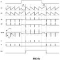
- High pass filters 91 and 92 allow to obtain respectively at each output nodes B1 and B2 of the isolation capacitors 61 and 62 successive peak pulses of same orientations while the data signal D remains constant as shown in Fig.4b .
- To obtain such pulses after a capacitive isolation is impossible when using square or sinusoidal pulses. Indeed, when using square pulses, the high pass filter will always transmit a fast rising edge followed by a fast falling edge and so on, making it impossible to transmit successive data peaks of same orientation.
- the sawtooth signal's logic value is defined by the orientation of the fast edge of the sawtooth signal. For example, a fast rising edge will define a logical 1 when a fast falling edge will define a logical 0.
- the sawtooth signal On a first channel 71 the sawtooth signal has the same logic value than said input signal D, such that said sawtooth signal at node A1 has a fast falling edge followed by a slow rising edge when input signal D is 0 and a fast rising edge followed by a slow falling edge when input signal D is 1.
- the sawtooth signal On a second channel 72 the sawtooth signal has an opposite logic value than said input signal D, such that said sawtooth signal at node A2 has a fast rising edge followed by a slow falling edge when input signal D is 0 and a fast falling edge followed by a slow rising edge when input signal D is 1.
- said first sawtooth signal When said first sawtooth signal is applied to node A1, said first sawtooth signal is filtered such that, at node B1, only fast transients of the said first sawtooth signal will form short pulses with large magnitude with orientation corresponding to the derivative of the input pulse.
- a fast rising curve slope occurs at input node A1
- a short positive pulse with large magnitude occurs at node B1.
- a fast falling curve slope occurs at input node A1
- a short negative pulse with large magnitude occurs at node B1.
- the input signal is composed of sawtooth pulses, all fast edges are of same variation until the value of D is changed.
- sawtooth signal at node A1 will be composed of fast rising edges followed by slow falling slopes such that at node B1, the filtering will produce successive short positive pulses with large magnitude followed by long and very small pulses of negative values as represented in Fig.4b .
- the sawtooth signal at A1 is composed of fast falling edges followed by slow rising slopes such that at node B1, the filtering will produce successive short negative pulses with large magnitude followed by long and very small pulses of positive values.
- the ratio of the duration of the fast falling/fast rising edges to the corresponding slow rising/slow falling edges is selected in order that the corresponding filtered pulse have sufficiently different amplitudes in order for the threshold comparators to transmit only when the differences between signals at nodes B1 and B2 are larger than a threshold.
- This ratio may be smaller than 1/2, 1/5 or even 1/10.
- the differential link 80 comprises two channels 71 and 72 of inversed logic, when a logic signal 1 is sent to the first line of the differential link, a logic signal 0 is sent to the second line of the differential link and when a logic signal 0 is sent to the first line of the differential link, a logic signal 1 is sent to the second line of the differential link.
- nodes A1 and A2, respectively B1 and B2 will receive signals of complementary logic values.
- the system will auto correct itself after a maximum time delay of one modulated signal period of time T0 which is also the time between two fast edges of the sawtooth signals. This allows to drastically reduce the time during which the system may provide a wrong information.
- Said sawtooth modulators STM1 51 receives said first command signals 41. It is configured for providing a first sawtooth signal at a node A1, output of STM1.
- Said first sawtooth signal at node A1 is composed of a fast rising edge triggered by a rising edge of the clock signal CLK, followed by a slow falling edge when D equals 1 and is composed of a fast falling edge triggered by a rising edge of the clock signal CLK, followed by a slow rising edge, when D equals 0.
- the said second sawtooth modulator STM2 52 is configured for receiving said second command signals 42, and for providing a second sawtooth signal at a node A2, output of STM2.
- Said second sawtooth signal is composed of a fast falling edge triggered by a rising edge of the clock signal CLK, followed by a slow rising edge, when D equals 1 and a fast rising edge triggered by a rising edge of the clock signal CLK, followed by a slow falling edge, when D equals 0 such that the two said sawtooth signals provide data information of inversed logic.
- Sawtooth modulators 51 and 52 can be classically implemented for example but non exclusively, in CMOS technology, making use of transistors or micro-electromechanical switches as gates.
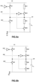
- a generic implementation using ideal switches or low-impedance switches is presented on figure Fig.6a and 6b .
- said first sawtooth modulator STM1 51 may comprise
- the current limiting dipoles ILU1 and ILD1 may either be current sources or resistors or a combination thereof.
- the values of these components and of the capacitor Cp1 are such that within the slow rising or falling edge, the sawtooth signals reaches at least 80% of V1 or reaches less than 20% of V1 respectively.
- Cp1 can be either a specific capacitor or a parasitic capacitance resulting from the technology used. A parasitic capacitance may result, e.g. from the circuit layout, the assembly such as bonding or connection.
- SU1 is set to close said switch LU1 such that the capacitance Cp1 is promptly charged to V1 through LU1, while SD1 is set to open switch LD1.
- W1 is set to close said switch MU1 such that the capacitance Cp1 is charged to V1 through MU1 and ILU1, while SD1 is set to open LD1 and SU1 is set to open LU1.
- SD1 is set to close said switch LD1 such that the capacitance Cp1 promptly discharge to ground G1 through LD1 while SU1 is set to open switch LU1.
- W1 is set to close said switch MD1 such that the capacitance Cp1 is discharged to G1 through MD1 and ILD1, while SD1 is set to open LD1 and SU1 is set to open LU1.
- said second sawtooth modulator STM2 52 may comprise
- the current limiting dipoles ILU2 and ILD2 may either be current sources or resistors or a combination thereof.
- the values of these components and of the capacitor Cp2 are such that within the slow rising or falling edge, the sawtooth signals reaches at least 80% of V1 or is less than 20% of V1 respectively.
- Cp2 can be either a specific capacitor or a parasitic capacitance from a technology. A parasitic capacitance may result, e.g. from the circuit layout, the assembly such as bonding or connection.
- SU2 is set to close said switch LU2 such that the capacitance Cp2 is promptly charged to V1 through LU2, while SD2 set to open switch LD2.
- W2 is set to close said switch MU2 such that the capacitance Cp2 is charged to V1 through MU2 and ILU2, while SD2 is set to open LD2 and SU2 is set to open LU2.
- SD2 is set to close said switch LD2 such that the capacitance Cp2 promptly discharge to ground G1 through LD2 while SU2 is set to open switches LU2.
- W2 is set to close said switch MD2 such that the capacitance Cp2 is discharged to G1 through MD2 and ILD2, while SD2 is set to open LD2 and SU2 is set to open LU2.
- a first threshold comparator 121 having a first input connected to said node B1, and a second input connected to said node B2, produces a logical 1 output S when the difference between the value of its first input exceeds its second input by a threshold Th1, and logical 0 output otherwise such that only positive B1-B2 pulses larger than the threshold Th1 will generate a logical 1 pulse at output S.
- a second threshold comparator 122 having a first input connected to said node B2, and a second input connected to said node B1, produces a logical 1 output R when its first input exceeds its second input by a threshold Th2, and a logical 0 output otherwise such that only positive B2-B1 pulses larger than the threshold Th2 will generate la logical 1 pulse at the output R.
- These two threshold comparators allow to obtain non interleaved successive digital pulses at a frequency of the clock signal CLK, only on output S when input signal D is set to logic 1 and only on output R when input signal is set to 0. This allows the system to be set in the correct mode according to the channel S or R from where the fast output signal comes from.
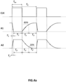
- Fig.4a represents typical signals at nodes A1 and A2 of the isolator of Fig. 3a or 3b , in dependence of the clock signal CLK, when digital signal D equals 0.
- the duration T1 of this down transition is very short because the resistance of the discharge circuit, including LD1 is low.
- T on the clock signal remains on
- A1 remains low (Ground G1) in a plateau for a duration T2.
- the parameters of these circuits are selected in order that the durations of the fast falling edge T1, fast rising edge T1' are significantly shorter than the durations of the slow rising edge T3 and slow falling edge T3', respectively. This may be performed by adjusting the value of a resistor for ILU1 and ILU2 or of capacitors C p1 and C p2 . Also the period of the clock T 0 and the pulse width T on may be selected in order that enough time is given during period T3 for the signal A1 to rise to at least 80% of V1 before the next clock pulse occurs.
- Fig.4b represents typical data pulses used to carry information at specific nodes of the circuit of Fig.3 .
- the signals represented relate to a case where the rising/falling edges are very fast (T1 and T1' nearly zero), The clock pulse width Ton, very short (T2 nearly zero) and T4 nearly zero.
- Input signal D is a classical square digital signal carrying the information to be transmitted through the digital isolator.
- Specific sawtooth signal at node A1 is used to transmit information through the isolation capacitor 61 and sawtooth signal at node A2 is used to transmit information through the isolation capacitor 62.
- Particular signals are found at node B1 and B2 corresponding respectively to signals at node A1 and A2 filtered by the high pass filters 91 and 92.
- the signal at node B1 is composed of successive pulses with a frequency corresponding to the clock frequency of the clock signal CLK. These pulses are positive with large magnitude when digital signal D is set to logic 1 and negative with large magnitude when digital signal D is set to logical 0.
- the signal at node B2 is composed of successive pulses with a frequency corresponding to the clock frequency of the clock signal CLK. These pulses are negative with large magnitude when digital signal D is set to logic 1 and positive with large magnitude when digital signal D is set to logical 0.
- the threshold comparator 121 At the output of the threshold comparator 121, only the difference between signals at nodes B1 and B2 that is greater than the threshold Th1 is transmitted at node S and at the output of the threshold comparator 122, only the difference between signals at nodes B2 and B1 that is greater than the threshold Th2 is transmitted at node R such that pulses appear at node S only when said input signal D is set to logical 1 and pulses appear at node R only when said input signal D is set to logical 0 such that the two signals Sand R are not interleaved.
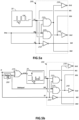
- Fig.5a, 5b , 5c are embodiments of said logic module 20 for use in a digital insulator according to embodiments of the invention.
- Said logic module 20 is composed of a clock generator 30 with an output delivering a clock signal CLK at node CK and a command interface CMD 190 for receiving digital signals at input nodes DD, CK and ID. Node ID is for receiving said input signal D.
- Said command interface CMD 190 is composed of:
- said nodes DD and ID are connected to the input of the digital isolator for receiving digital signal D.
- digital output signal S and R are not synchronized with the input signal D.
- the demodulated signal After demodulation of the output signals Sand R, for example by using an RS gate, the demodulated signal will present a small delay and a jitter.
- said logic module 20 is configured for providing first command signals to said first sawtooth modulator STM1 51, said first command signals comprising logical signals SU1, SD1 and W1, and for providing second command signals to said second sawtooth modulator STM2 52, said second command signals comprising logical signals SU2, SD2 and W2
- an anti-jitter solution is proposed characterized in that said logic module 20 comprises means for disabling the clock generator 30 at a transition of the digital signal D, and for re-enabling synchronously the clock generator after a delay TD afterwards. Such disabling is performed for downward and upward transitions of digital signal D.
- the delay TD is preferably larger than 0.5*T0, e.g. 0.6 or 0.7*T0, and more preferably larger than 0.8*T0.
- said logic module 20 is composed of:
- said logic module 20 is configured for providing first command signals to said first sawtooth modulator STM1 51, said first command signals comprising logical signals SU1, SD1 and W1, and for providing second command signals to said second sawtooth modulator STM2 52, said second command signals comprising logical signals SU2, SD2 and W2, said logical module comprising means for determining a digital signal Ddelayed, being digital signal D delayed by a duration equal to or longer than 0.8*T0
- input data D is internally delayed by a delay TD equal to or larger than T0 *0.8 to define a preset time lapse whenever the state of D is toggling.
- signals at node A1 and node A2 are preset to the correct initial state without applying any fast transition during this preset time lapse.
- the correct sawtooth signal fast transient can be applied on nodes A1 and A2. This introduces a constant delay of about TD in the transmission, but the jitter is reduced to close to zero on demodulated S and R signals with reference to the input data D.
- said logic module 20 is adapted for receiving a second digital signal D1 characterized in that said logic module 20 may comprise additional means for disabling the clock generator 30 when additional digital signal D1 is equal to logical 0.
- an additional digital signal D1 with reference to a first ground G1 is used as input digital signal, and said input signal D, with reference to said first ground G1, is used as a selector for sending a corresponding signal of said additional digital signal D1 on output R or output S, with reference to a second ground G2, depending on the logic value of said signal D.
- said logic module 20 is composed of:
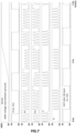
- Fig.7 show results of simulation of the anti-jitter embodiment of the invention.
- Input signal D between 0 V and 3 V with respect to ground G1, is transmitted without error to signal OUT, with constant delay TD, between 0 V and 3 V with respect to ground G2.
- the low impedance controllable switches, and medium impedance controllable switches used in the invention may be implemented in various ways, such, for example with MOSFETS, bipolar or any other kind of transistors or any kind of device that can modulate a conduction channel or any mechanical switching .
Landscapes
- Engineering & Computer Science (AREA)
- Power Engineering (AREA)
- Computer Networks & Wireless Communication (AREA)
- Signal Processing (AREA)
- Computer Hardware Design (AREA)
- Physics & Mathematics (AREA)
- Computing Systems (AREA)
- General Engineering & Computer Science (AREA)
- Mathematical Physics (AREA)
- General Physics & Mathematics (AREA)
- Dc Digital Transmission (AREA)
- Manipulation Of Pulses (AREA)
Claims (16)
- Digitaler Isolator (10) zum Empfangen eines digitalen Signals D unter Bezugnahme auf eine erste Masse G1 und Liefern entsprechender Signale an einen Ausgangsknoten R und Ausgangsknoten S unter Bezugnahme auf eine zweite Masse G2, umfassend- ein Logikmodul (20) zum Empfangen des digitalen Signals D und zum Liefern eines ersten (41) und zweiten (42) Befehlssignals, wobei das Logikmodul (20) einen Taktgenerator (30) umfasst, der ein Taktsignal CLK mit einer Periode T0 generiert;- einen ersten Sägezahnmodulator (51) STM1 zum Empfangen der ersten Befehlssignale (41) und konfiguriert zum Liefern eines ersten Sägezahnsignals an einen Knoten A1, wobei das erste Sägezahnsignal eine durch eine steigende Flanke des Taktsignals CLK ausgelöste schnell ansteigende Flanke aufweist, gefolgt von einer langsam fallenden Flanke, wenn D gleich 1 ist und das erste Sägezahnsignal eine durch eine steigende Flanke des Taktsignals CLK ausgelöste schnell fallende Flanke aufweist, gefolgt von einer langsam ansteigenden Flanke, wenn D gleich 0 ist;- einen zweiten Sägezahnmodulator (52) STM2 zum Empfangen der zweiten Befehlssignale (42) und konfiguriert zum Liefern eines zweiten Sägezahnsignals an einen Knoten A2, wobei das zweite Sägezahnsignal eine durch eine steigende Flanke des Taktsignals CLK ausgelöste schnell fallende Flanke aufweist, gefolgt von einer langsam ansteigenden Flanke, wenn D gleich 1 ist, und eine durch eine steigende Flanke des Taktsignals CLK ausgelöste schnell ansteigende Flanke, gefolgt von einer langsam fallenden Flanke, wenn D gleich 0 ist;- einen ersten Trennkondensator (61), der an den Knoten A1 und an einen Knoten B1 angeschlossen ist;- einen ersten Dipol (101) Z1, der zwischen den Knoten B1 und eine Vorspannungsquelle (110) unter Bezugnahme auf eine zweite Masse G2 geschaltet ist;- einen zweiten Trennkondensator (62), der an den Knoten A2 und an einen Knoten B2 angeschlossen ist;- einen zweiten Dipol (102) Z2, der zwischen den Knoten B2 und die Vorspannungsquelle (110) geschaltet ist;- einen ersten Schwellwertvergleicher (121) mit einem an den Knoten B1 angeschlossenen ersten Eingang und einem an den Knoten B2 angeschlossenen zweiten Eingang,
Erzeugen eines Ausgangs S mit einer logischen 1, wenn sein erster Eingang seinen zweiten Eingang um einen Schwellwert Th1 übersteigt, und ansonsten einen Ausgang mit einer logischen 0;- einen zweiten Schwellwertvergleicher (122) mit einem an den Knoten B2 angeschlossenen ersten Eingang und einem an den Knoten B1 angeschlossenen zweiten Eingang,
Erzeugen eines Ausgangs R mit einer logischen 1, wenn sein erster Eingang seinen zweiten Eingang um einen Schwellwert Th2 übersteigt, und ansonsten einem Ausgang mit einer logischen 0. - Digitaler Isolator (10) nach Anspruch 1, dadurch gekennzeichnet, dass die Dauern der langsam steigenden Flanken und/oder der langsam fallenden Flanken an den Knoten A1 und/oder A2 jeweils mindestens das Doppelte der Dauern der entsprechenden schnell fallenden Flanken und/oder schnell ansteigenden Flanken sind.
- Digitaler Isolator (10) nach Anspruch 1 oder 2, dadurch gekennzeichnet, dass das Taktsignal CLK eine Impulsbreite aufweist, die kürzer ist als T0/3.
- Digitaler Isolator (10) nach einem der Ansprüche 1 bis 3, dadurch gekennzeichnet, dass das Logikmodul (20) Mittel zum Deaktivieren des Taktgenerators (30) bei einem Übergang des digitalen Signals D und zum Reaktivieren des Taktgenerators nach einer Verzögerung größer TD umfasst.
- Digitaler Isolator (10) nach Anspruch 4, dadurch gekennzeichnet, dass die Verzögerung TD größer ist als 0,5*T0, 0,6*T0, 0,7*T0, 0,8*T0 oder T0.
- Digitaler Isolator (10) nach Anspruch 4 oder 5, dadurch gekennzeichnet, dass er ausgelegt ist zum Empfangen eines zusätzlichen digitalen Signals D1 unter Bezugnahme auf die erste Masse G1, dadurch gekennzeichnet, dass das Logikmodul (20) zusätzliche Mittel zum Deaktivieren des Taktgenerators (30), wenn das zusätzliche digitale Signal D1 gleich einer logischen 0 ist, umfasst.
- Digitaler Isolator (10) nach einem der Ansprüche 1 bis 3, dadurch gekennzeichnet, dass das Logikmodul (20) konfiguriert ist zum Liefern erster Befehlssignale (41) an den ersten Sägezahnmodulator (51) STM1, wobei die ersten Befehlssignale (41) logische Signale SU1, SD1 und W1 umfassen, und zum Liefern zweiter Befehlssignale (42) an den zweiten Sägezahnmodulator (52) STM2, wobei die zweiten Befehlssignale Logiksignale SU2, SD2 und W2 umfassen, wobei- SU1 gleich 1 ist, wenn D gleich 0 ist, und ansonsten gleich dem Kehrwert des Taktsignals;- SD1 gleich dem Taktsignal CLK ist, wenn D gleich 0 ist, und ansonsten gleich 0;- W1 gleich 0 oder gleich CLK ist, wenn D gleich 0, und gleich 1 oder gleich not(CLK) ist, wenn D gleich 1,- SU2 gleich not(SD1) ist;- SD2 gleich not(SU1) ist;- W2 gleich not(W1) ist.
- Digitaler Isolator (10) nach Anspruch 7, dadurch gekennzeichnet, dass er einen SR-Zwischenspeicher umfasst, wobei die Signale an Ausgangsknoten R und S an entsprechende Eingänge des SR-Zwischenspeichers angeschlossen sind.
- Digitaler Isolator (10) nach Ansprüchen 4 oder 5, dadurch gekennzeichnet, dass das Logikmodul (20) konfiguriert ist zum Liefern erster Befehlssignale (41) an den ersten Sägezahnmodulator (51) STM1, wobei die ersten Befehlssignale (41) logische Signale SU1, SD1 und W1 umfassen, und zum Liefern zweiter Befehlssignale (42) an den zweiten Sägezahnmodulator (52) STM2, wobei die zweiten Befehlssignale (42) Logiksignale SU2, SD2 und W2 umfassen, wobei das Logikmodul (20) Mittel zum Bestimmen eines digitalen Signals Ddelayed umfasst, wobei das digitale Signal D um eine Dauer länger oder gleich 0,8*T0 verzögert ist, wobei- SU1 gleich not(CLK) ist, wenn D gleich 1 und Ddelayed gleich 1 ist, und ansonsten SU1 gleich 1 ist;- SD1 gleich dem Taktsignal CLK ist, wenn D gleich 0 ist und Ddelayed gleich 0 ist, und ansonsten SD1 gleich 0 ist;- W1 gleich 0 oder gleich CLK ist, wenn D gleich 0 und Ddelayed gleich 0 ist, W1 gleich 1 oder gleich not(CLK) ist, wenn D gleich 1 und Ddelayed gleich 1, W1 gleich 0, wenn D gleich 0 und Ddelayed gleich 1 ist, W1 gleich 1 ist, wenn D gleich 1 und Ddelayed gleich 0 ist; wobei- SU2 gleich not(SD1) ist;- SD2 gleich not(SU1) ist;- W2 gleich not(W1) ist.
- Digitaler Isolator (10) nach Anspruch 6, dadurch gekennzeichnet, dass das Logikmodul (20) konfiguriert ist zum Liefern erster Befehlssignale (41) an den ersten Sägezahnmodulator (51) STM1, wobei die ersten Befehlssignale (41) logische Signale SU1, SD1 und W1 umfassen, und zum Liefern zweiter Befehlssignale (42) an den zweiten Sägezahnmodulator (52) STM2, wobei die zweiten Befehlssignale (42) Logiksignale SU2, SD2 und W2 umfassen, wobei das Logikmodul Mittel zum Bestimmen eines digitalen Signals Ddelayed umfasst, wobei das digitale Signal D um eine Dauer länger oder gleich 0,8*T0 verzögert ist, wobei- SU1 gleich not(CLK) ist, wenn D gleich 1, Ddelayed gleich 1 und D1 gleich 1, und ansonsten SU1 gleich 1 ist;- SD1 gleich dem Taktsignal CLK ist, wenn D gleich 0 ist, Ddelayed gleich 0 ist und D1 gleich 1, und ansonsten SD1 gleich 0 ist;- W1 gleich 0 oder gleich CLK ist, wenn D gleich 0, Ddelayed gleich 0 und D1 gleich 1, wobei W1 gleich 1 oder gleich not(CLK) ist, wenn D gleich 1, Ddelayed gleich 1 und D1 gleich 1, wobei W1 gleich 0 ist, wenn D gleich 0 ist, Ddelayed gleich 0 und D1 gleich 0, wobei W1 gleich 1 ist, wenn D gleich 1, Ddelayed gleich 1 und D1 gleich 0; wobei- SU2 gleich not(SD1) ist;- SD2 gleich not(SU1) ist;- W2 gleich not(W1) ist.
- Digitaler Isolator nach einem der vorhergehenden Ansprüche, dadurch gekennzeichnet, dass der erste Sägezahnmodulator STM1 51 umfasst- einen ersten niederimpedanten steuerbaren Schalter LU1, der zwischen eine erste Stromversorgungsspannung V1 und den Ausgangsknoten A1 geschaltet ist, der geschlossen ist, wenn das Befehlssignal SU1 gleich 0 ist, und ansonsten offen ist;- einen zweiten niederimpedanten steuerbaren Schalter LD1, der zwischen den Knoten A1 und die erste Masse G1 geschaltet ist, der geschlossen ist, wenn das Befehlssignal SD1 gleich 1 ist, und ansonsten offen ist;- einen ersten steuerbaren Schalter MU1, der in Reihe mit einem strombegrenzenden Dipol ILU1 zwischen die erste Stromversorgungsspannung V1 und den Knoten A1 geschaltet ist, wobei der erste steuerbare Schalter MU1 offen ist, wenn das Befehlssignal W1 gleich 1 ist, und ansonsten geschlossen ist;- einen zweiten steuerbaren Schalter MD1, der in Reihe mit einem strombegrenzenden Dipol ILD1 zwischen den Knoten A1 und die erste Masse G1 geschaltet ist, wobei der zweite steuerbare Schalter geschlossen ist, wenn das Befehlssignal W1 gleich 1 ist, und ansonsten offen ist;- einen Kondensator Cp1 zwischen dem Knoten A1 und Masse G1.
- Digitaler Isolator nach einem der vorhergehenden Ansprüche, dadurch gekennzeichnet, dass der zweite Sägezahnmodulator STM2 52 umfasst- einen ersten niederimpedanten steuerbaren Schalter LU2, der zwischen eine erste Stromversorgungsspannung V1 und den Ausgangsknoten A2 geschaltet ist, der geschlossen ist, wenn das Befehlssignal SU2 gleich 0 ist, und ansonsten offen ist;- einen zweiten niederimpedanten steuerbaren Schalter LD2, der zwischen den Knoten A2 und die erste Masse G1 geschaltet ist, der geschlossen ist, wenn das Befehlssignal SD2 gleich 1 ist, und ansonsten offen ist;- einen ersten steuerbaren Schalter MU2, der in Reihe mit einem strombegrenzenden Dipol ILU2 zwischen die erste Stromversorgungsspannung V1 und den Knoten A2 geschaltet ist, wobei der erste steuerbare Schalter offen ist, wenn das Befehlssignal W2 gleich 1 ist, und ansonsten geschlossen ist;- einen zweiten steuerbaren Schalter MD2, der in Reihe mit einem strombegrenzenden Dipol ILD2 zwischen den Knoten A2 und die erste Masse G1 geschaltet ist, wobei der zweite steuerbare Schalter geschlossen ist, wenn das Befehlssignal W2 gleich 1 ist, und ansonsten offen ist;- einen Kondensator Cp2 zwischen dem Knoten A2 und Masse G1.
- Verfahren zum Isolieren eines digitalen Signals D unter Bezugnahme auf eine erste Masse G1 und Liefern entsprechender Signale an einen Ausgangsknoten R und einen Ausgangsknoten S unter Bezugnahme auf eine zweite Masse G2, umfassend die folgenden Schritte:- Empfangen des digitalen Signals D und Liefern eines ersten (41) und zweiten (42) Befehlssignals, Generieren eines Taktsignals CLK mit einer Periode T0;- Empfangen der ersten Befehlssignale (41) und Liefern eines ersten Sägezahnsignals an einen Knoten A1, wobei das erste Sägezahnsignal eine durch eine steigende Flanke des Taktsignals CLK ausgelöste schnell steigende Flanke aufweist, gefolgt von einer langsam fallenden Flanke, wenn D gleich 1, und das erste Sägezahnsignal eine durch eine steigende Flanke des Taktsignals CLK ausgelöste schnell fallende Flanke aufweist, gefolgt von einer langsam fallenden Flanke, wenn D gleich 0;- Empfangen der zweiten Befehlssignale (42) und Liefern eines zweiten Sägezahnsignals an einen Knoten A2, wobei das zweite Sägezahnsignal eine durch eine steigende Flanke des Taktsignals CLK ausgelöste schnell fallende Flanke aufweist, gefolgt von einer langsam steigenden Flanke, wenn D gleich 1 ist, und eine durch eine steigende Flanke des Taktsignals CLK ausgelöste schnell steigende Flanke, gefolgt von einer langsam fallenden Flanke, wenn D gleich 0;- Liefern des ersten Sägezahnsignals an einen an den Knoten A1 angeschlossen ersten Trennkondensator (61) und Erhalten eines ersten isolierten Signals an einem Knoten B1 des ersten Trennkondensators (61) ;- Hochpassfilterung des ersten isolierten Signals, wobei ein Hochpassfilter durch den ersten Trennkondensator und einen ersten Dipol (101) Z1 gebildet wird, geschaltet zwischen den Knoten B1 und eine Vorspannungsquelle (110) unter Bezugnahme auf eine zweite Masse G2;- Liefern des zweiten Sägezahnsignals an einen mit dem Knoten A2 verbundenen zweiten Trennkondensator (62) und Erhalten eines zweiten isolierten Signals an einem Knoten B2 des zweiten Trennkondensators (62);- Hochpassfilterung des zweiten isolierten Signals, wobei ein Hochpassfilter durch den zweiten Trennkondensator (62) und einen zweiten Dipol (102) Z2 gebildet ist, geschaltet zwischen den Knoten B2 und die Vorspannungsquelle (110) unter Bezugnahme auf eine zweite Masse G2;- Liefern des ersten und zweiten isolierten Signals an einen ersten Schwellwertvergleicher (121), der einen Ausgangs S produziert, der eine logische 1 ist, wenn das erste isolierte Signal das zweite isolierte Signal um einen Schwellwert Th1 übersteigt, und ansonsten eine logische 0;- Liefern des ersten und zweiten isolierten Signals an einen zweiten Schwellwertvergleicher (122), der einen Ausgang R produziert, der eine logische 1 ist, wenn das zweite isolierte Signal das erste isolierte Signal um einen Schwellwert Th2 übersteigt, und ansonsten einen Ausgang mit einer logischen 0.
- Verfahren nach Anspruch 13, dadurch gekennzeichnet, dass die Dauern der langsam steigenden Flanken und/oder der langsam fallenden Flanken an den Knoten A1 und/oder A2 jeweils mindestens das Doppelte der Dauern der entsprechenden schnell fallenden Flanken und/oder schnell ansteigenden Flanken sind.
- Verfahren nach Anspruch 13 oder 14, dadurch gekennzeichnet, dass das Taktsignal CLK eine Impulsbreite aufweist, die kürzer ist als T0/3.
- Verfahren nach einem der Ansprüche 13 bis 15, dadurch gekennzeichnet, dass es den Schritt des Lieferns der Signale an Ausgangsknoten R und S an entsprechende Eingänge eines SR-Zwischenspeichers umfasst.
Priority Applications (1)
| Application Number | Priority Date | Filing Date | Title |
|---|---|---|---|
| EP23179008.0A EP4254803B1 (de) | 2018-07-10 | 2019-07-09 | Digitaler isolator |
Applications Claiming Priority (2)
| Application Number | Priority Date | Filing Date | Title |
|---|---|---|---|
| EP18182754 | 2018-07-10 | ||
| PCT/EP2019/068444 WO2020011801A1 (en) | 2018-07-10 | 2019-07-09 | Digital isolator |
Related Child Applications (1)
| Application Number | Title | Priority Date | Filing Date |
|---|---|---|---|
| EP23179008.0A Division EP4254803B1 (de) | 2018-07-10 | 2019-07-09 | Digitaler isolator |
Publications (3)
| Publication Number | Publication Date |
|---|---|
| EP3821574A1 EP3821574A1 (de) | 2021-05-19 |
| EP3821574B1 true EP3821574B1 (de) | 2023-06-14 |
| EP3821574C0 EP3821574C0 (de) | 2023-06-14 |
Family
ID=63047100
Family Applications (2)
| Application Number | Title | Priority Date | Filing Date |
|---|---|---|---|
| EP19736393.0A Active EP3821574B1 (de) | 2018-07-10 | 2019-07-09 | Digitaler isolator |
| EP23179008.0A Active EP4254803B1 (de) | 2018-07-10 | 2019-07-09 | Digitaler isolator |
Family Applications After (1)
| Application Number | Title | Priority Date | Filing Date |
|---|---|---|---|
| EP23179008.0A Active EP4254803B1 (de) | 2018-07-10 | 2019-07-09 | Digitaler isolator |
Country Status (2)
| Country | Link |
|---|---|
| EP (2) | EP3821574B1 (de) |
| WO (1) | WO2020011801A1 (de) |
Families Citing this family (3)
| Publication number | Priority date | Publication date | Assignee | Title |
|---|---|---|---|---|
| EP3846345B1 (de) * | 2019-12-31 | 2022-08-03 | Vddtech | Schneller digitaler isolator |
| US11792051B2 (en) * | 2020-07-17 | 2023-10-17 | Texas Instruments Incorporated | Multi-channel digital isolator with integrated configurable pulse width modulation interlock protection |
| EP4113845A1 (de) * | 2021-06-29 | 2023-01-04 | STMicroelectronics S.r.l. | Senderschaltung, entsprechende isolierte treibervorrichtung, elektronisches system und verfahren zum codieren eines pulsbreitenmodulierten signals in ein differenzielles gepulstes signal |
Family Cites Families (5)
| Publication number | Priority date | Publication date | Assignee | Title |
|---|---|---|---|---|
| CN1258406A (zh) | 1997-03-31 | 2000-06-28 | 株式会社日立制作所 | 使用容性绝缘壁的调制解调器装置和绝缘耦合器以及调制解调器装置中使用的集成电略 |
| US6144326A (en) * | 1997-04-22 | 2000-11-07 | Silicon Laboratories, Inc. | Digital isolation system with ADC offset calibration |
| US8451032B2 (en) * | 2010-12-22 | 2013-05-28 | Silicon Laboratories Inc. | Capacitive isolator with schmitt trigger |
| US9698728B2 (en) | 2012-12-13 | 2017-07-04 | Texas Instruments Incorporated | Digital isolator |
| US9998301B2 (en) * | 2014-11-03 | 2018-06-12 | Analog Devices, Inc. | Signal isolator system with protection for common mode transients |
-
2019
- 2019-07-09 WO PCT/EP2019/068444 patent/WO2020011801A1/en not_active Ceased
- 2019-07-09 EP EP19736393.0A patent/EP3821574B1/de active Active
- 2019-07-09 EP EP23179008.0A patent/EP4254803B1/de active Active
Also Published As
| Publication number | Publication date |
|---|---|
| EP4254803B1 (de) | 2026-05-06 |
| EP4254803A3 (de) | 2024-01-03 |
| EP3821574C0 (de) | 2023-06-14 |
| EP4254803A2 (de) | 2023-10-04 |
| WO2020011801A1 (en) | 2020-01-16 |
| EP3821574A1 (de) | 2021-05-19 |
Similar Documents
| Publication | Publication Date | Title |
|---|---|---|
| US7923710B2 (en) | Digital isolator with communication across an isolation barrier | |
| US20240421820A1 (en) | Fast digital isolator | |
| US10840960B1 (en) | Demodulator/detector for digital isolators | |
| US10038403B2 (en) | Digital isolator | |
| EP3821574B1 (de) | Digitaler isolator | |
| KR102468237B1 (ko) | 디지털 격리기들을 위한 리시버 프론트 엔드 | |
| EP2798742B1 (de) | Schwankungsreduzierung ein einem weitergeleiteten takt | |
| EP3291446A1 (de) | Galvanische isolierungsschaltung, entsprechendes system und verfahren | |
| KR102422590B1 (ko) | 격리기 제품을 위한 수신기 중간 가변 이득 스테이지 | |
| CN108988831A (zh) | 电容式数字隔离芯片及其调制解调方法 | |
| US20220385258A1 (en) | Isolation communications channel using direct demodulation and data-edge encoding | |
| SI21435A (sl) | Izolacijski vmesnik s kapacitivno bariero in postopek prenosa signala s pomočjo takega izolacijskega vmesnika | |
| EP3248345B1 (de) | Verfahren und vorrichtung zur abschwächung von baseline-wandern bei einer wechselstromgekoppelten verbindung | |
| US8760225B1 (en) | BiCMOS gate driver for class-S radio frequency power amplifier | |
| TWI634767B (zh) | 通訊系統與資料通訊方法 | |
| EP2282405B1 (de) | Signalkommunikationsvorrichtung und entsprechender Empfänger | |
| KR20150014444A (ko) | 채널(베리언트) 내 왜곡을 보상하는 무선 용량 신호 수신 및 송신 시스템, 방법 및 장치 | |
| US7142014B1 (en) | High frequency XOR with peaked load stage | |
| US10044345B2 (en) | Circuit for improving clock rates in high speed electronic circuits using feedback based flip-flops | |
| Aggarwal | Low power analog front end design for 112 Gbps PAM-4 SERDES receiver | |
| US20260046174A1 (en) | Full duplex digital isolator | |
| EP2282406B1 (de) | Signalempfänger mit Störungsunterdrückung | |
| EP4664774A1 (de) | Galvanisch isolierte kommunikationsschaltung und verfahren zur übertragung eines datensignals über eine kapazitive isolationsbarriere | |
| US7733131B2 (en) | Signal presence detector | |
| CN107835013A (zh) | 一种用于脉冲码型发生器的定时电路 |
Legal Events
| Date | Code | Title | Description |
|---|---|---|---|
| STAA | Information on the status of an ep patent application or granted ep patent |
Free format text: STATUS: UNKNOWN |
|
| STAA | Information on the status of an ep patent application or granted ep patent |
Free format text: STATUS: THE INTERNATIONAL PUBLICATION HAS BEEN MADE |
|
| PUAI | Public reference made under article 153(3) epc to a published international application that has entered the european phase |
Free format text: ORIGINAL CODE: 0009012 |
|
| STAA | Information on the status of an ep patent application or granted ep patent |
Free format text: STATUS: REQUEST FOR EXAMINATION WAS MADE |
|
| 17P | Request for examination filed |
Effective date: 20210121 |
|
| AK | Designated contracting states |
Kind code of ref document: A1 Designated state(s): AL AT BE BG CH CY CZ DE DK EE ES FI FR GB GR HR HU IE IS IT LI LT LU LV MC MK MT NL NO PL PT RO RS SE SI SK SM TR |
|
| DAV | Request for validation of the european patent (deleted) | ||
| DAX | Request for extension of the european patent (deleted) | ||
| GRAP | Despatch of communication of intention to grant a patent |
Free format text: ORIGINAL CODE: EPIDOSNIGR1 |
|
| STAA | Information on the status of an ep patent application or granted ep patent |
Free format text: STATUS: GRANT OF PATENT IS INTENDED |
|
| INTG | Intention to grant announced |
Effective date: 20230111 |
|
| GRAS | Grant fee paid |
Free format text: ORIGINAL CODE: EPIDOSNIGR3 |
|
| GRAA | (expected) grant |
Free format text: ORIGINAL CODE: 0009210 |
|
| STAA | Information on the status of an ep patent application or granted ep patent |
Free format text: STATUS: THE PATENT HAS BEEN GRANTED |
|
| AK | Designated contracting states |
Kind code of ref document: B1 Designated state(s): AL AT BE BG CH CY CZ DE DK EE ES FI FR GB GR HR HU IE IS IT LI LT LU LV MC MK MT NL NO PL PT RO RS SE SI SK SM TR |
|
| REG | Reference to a national code |
Ref country code: CH Ref legal event code: EP |
|
| REG | Reference to a national code |
Ref country code: DE Ref legal event code: R096 Ref document number: 602019031035 Country of ref document: DE |
|
| REG | Reference to a national code |
Ref country code: AT Ref legal event code: REF Ref document number: 1580042 Country of ref document: AT Kind code of ref document: T Effective date: 20230715 |
|
| U01 | Request for unitary effect filed |
Effective date: 20230623 |
|
| U07 | Unitary effect registered |
Designated state(s): AT BE BG DE DK EE FI FR IT LT LU LV MT NL PT SE SI Effective date: 20230630 |
|
| U20 | Renewal fee for the european patent with unitary effect paid |
Year of fee payment: 5 Effective date: 20230629 |
|
| REG | Reference to a national code |
Ref country code: LT Ref legal event code: MG9D |
|
| PG25 | Lapsed in a contracting state [announced via postgrant information from national office to epo] |
Ref country code: NO Free format text: LAPSE BECAUSE OF FAILURE TO SUBMIT A TRANSLATION OF THE DESCRIPTION OR TO PAY THE FEE WITHIN THE PRESCRIBED TIME-LIMIT Effective date: 20230914 Ref country code: ES Free format text: LAPSE BECAUSE OF FAILURE TO SUBMIT A TRANSLATION OF THE DESCRIPTION OR TO PAY THE FEE WITHIN THE PRESCRIBED TIME-LIMIT Effective date: 20230614 |
|
| PG25 | Lapsed in a contracting state [announced via postgrant information from national office to epo] |
Ref country code: RS Free format text: LAPSE BECAUSE OF FAILURE TO SUBMIT A TRANSLATION OF THE DESCRIPTION OR TO PAY THE FEE WITHIN THE PRESCRIBED TIME-LIMIT Effective date: 20230614 Ref country code: HR Free format text: LAPSE BECAUSE OF FAILURE TO SUBMIT A TRANSLATION OF THE DESCRIPTION OR TO PAY THE FEE WITHIN THE PRESCRIBED TIME-LIMIT Effective date: 20230614 Ref country code: GR Free format text: LAPSE BECAUSE OF FAILURE TO SUBMIT A TRANSLATION OF THE DESCRIPTION OR TO PAY THE FEE WITHIN THE PRESCRIBED TIME-LIMIT Effective date: 20230915 |
|
| PG25 | Lapsed in a contracting state [announced via postgrant information from national office to epo] |
Ref country code: SK Free format text: LAPSE BECAUSE OF FAILURE TO SUBMIT A TRANSLATION OF THE DESCRIPTION OR TO PAY THE FEE WITHIN THE PRESCRIBED TIME-LIMIT Effective date: 20230614 |
|
| PG25 | Lapsed in a contracting state [announced via postgrant information from national office to epo] |
Ref country code: IS Free format text: LAPSE BECAUSE OF FAILURE TO SUBMIT A TRANSLATION OF THE DESCRIPTION OR TO PAY THE FEE WITHIN THE PRESCRIBED TIME-LIMIT Effective date: 20231014 |
|
| PG25 | Lapsed in a contracting state [announced via postgrant information from national office to epo] |
Ref country code: SM Free format text: LAPSE BECAUSE OF FAILURE TO SUBMIT A TRANSLATION OF THE DESCRIPTION OR TO PAY THE FEE WITHIN THE PRESCRIBED TIME-LIMIT Effective date: 20230614 Ref country code: SK Free format text: LAPSE BECAUSE OF FAILURE TO SUBMIT A TRANSLATION OF THE DESCRIPTION OR TO PAY THE FEE WITHIN THE PRESCRIBED TIME-LIMIT Effective date: 20230614 Ref country code: RO Free format text: LAPSE BECAUSE OF FAILURE TO SUBMIT A TRANSLATION OF THE DESCRIPTION OR TO PAY THE FEE WITHIN THE PRESCRIBED TIME-LIMIT Effective date: 20230614 Ref country code: IS Free format text: LAPSE BECAUSE OF FAILURE TO SUBMIT A TRANSLATION OF THE DESCRIPTION OR TO PAY THE FEE WITHIN THE PRESCRIBED TIME-LIMIT Effective date: 20231014 Ref country code: CZ Free format text: LAPSE BECAUSE OF FAILURE TO SUBMIT A TRANSLATION OF THE DESCRIPTION OR TO PAY THE FEE WITHIN THE PRESCRIBED TIME-LIMIT Effective date: 20230614 |
|
| PG25 | Lapsed in a contracting state [announced via postgrant information from national office to epo] |
Ref country code: PL Free format text: LAPSE BECAUSE OF FAILURE TO SUBMIT A TRANSLATION OF THE DESCRIPTION OR TO PAY THE FEE WITHIN THE PRESCRIBED TIME-LIMIT Effective date: 20230614 |
|
| REG | Reference to a national code |
Ref country code: CH Ref legal event code: PL |
|
| PG25 | Lapsed in a contracting state [announced via postgrant information from national office to epo] |
Ref country code: MC Free format text: LAPSE BECAUSE OF FAILURE TO SUBMIT A TRANSLATION OF THE DESCRIPTION OR TO PAY THE FEE WITHIN THE PRESCRIBED TIME-LIMIT Effective date: 20230614 |
|
| REG | Reference to a national code |
Ref country code: DE Ref legal event code: R097 Ref document number: 602019031035 Country of ref document: DE |
|
| PG25 | Lapsed in a contracting state [announced via postgrant information from national office to epo] |
Ref country code: MC Free format text: LAPSE BECAUSE OF FAILURE TO SUBMIT A TRANSLATION OF THE DESCRIPTION OR TO PAY THE FEE WITHIN THE PRESCRIBED TIME-LIMIT Effective date: 20230614 |
|
| PLBE | No opposition filed within time limit |
Free format text: ORIGINAL CODE: 0009261 |
|
| STAA | Information on the status of an ep patent application or granted ep patent |
Free format text: STATUS: NO OPPOSITION FILED WITHIN TIME LIMIT |
|
| REG | Reference to a national code |
Ref country code: IE Ref legal event code: MM4A |
|
| PG25 | Lapsed in a contracting state [announced via postgrant information from national office to epo] |
Ref country code: CH Free format text: LAPSE BECAUSE OF NON-PAYMENT OF DUE FEES Effective date: 20230731 |
|
| 26N | No opposition filed |
Effective date: 20240315 |
|
| GBPC | Gb: european patent ceased through non-payment of renewal fee |
Effective date: 20230914 |
|
| PG25 | Lapsed in a contracting state [announced via postgrant information from national office to epo] |
Ref country code: IE Free format text: LAPSE BECAUSE OF NON-PAYMENT OF DUE FEES Effective date: 20230709 |
|
| PG25 | Lapsed in a contracting state [announced via postgrant information from national office to epo] |
Ref country code: GB Free format text: LAPSE BECAUSE OF NON-PAYMENT OF DUE FEES Effective date: 20230914 |
|
| U20 | Renewal fee for the european patent with unitary effect paid |
Year of fee payment: 6 Effective date: 20240605 |
|
| PG25 | Lapsed in a contracting state [announced via postgrant information from national office to epo] |
Ref country code: IE Free format text: LAPSE BECAUSE OF NON-PAYMENT OF DUE FEES Effective date: 20230709 Ref country code: GB Free format text: LAPSE BECAUSE OF NON-PAYMENT OF DUE FEES Effective date: 20230914 |
|
| U1H | Name or address of the proprietor changed after the registration of the unitary effect |
Owner name: NAVITAS SEMICONDUCTOR LIMITED; IE |
|
| U20 | Renewal fee for the european patent with unitary effect paid |
Year of fee payment: 7 Effective date: 20250606 |
|
| PG25 | Lapsed in a contracting state [announced via postgrant information from national office to epo] |
Ref country code: CY Free format text: LAPSE BECAUSE OF FAILURE TO SUBMIT A TRANSLATION OF THE DESCRIPTION OR TO PAY THE FEE WITHIN THE PRESCRIBED TIME-LIMIT; INVALID AB INITIO Effective date: 20190709 |
|
| PG25 | Lapsed in a contracting state [announced via postgrant information from national office to epo] |
Ref country code: HU Free format text: LAPSE BECAUSE OF FAILURE TO SUBMIT A TRANSLATION OF THE DESCRIPTION OR TO PAY THE FEE WITHIN THE PRESCRIBED TIME-LIMIT; INVALID AB INITIO Effective date: 20190709 |
|
| PG25 | Lapsed in a contracting state [announced via postgrant information from national office to epo] |
Ref country code: TR Free format text: LAPSE BECAUSE OF FAILURE TO SUBMIT A TRANSLATION OF THE DESCRIPTION OR TO PAY THE FEE WITHIN THE PRESCRIBED TIME-LIMIT Effective date: 20230614 |