EP3823046B1 - Lichterfassendes modul und elektronische vorrichtung mit verwendung davon - Google Patents
Lichterfassendes modul und elektronische vorrichtung mit verwendung davon Download PDFInfo
- Publication number
- EP3823046B1 EP3823046B1 EP20207159.3A EP20207159A EP3823046B1 EP 3823046 B1 EP3823046 B1 EP 3823046B1 EP 20207159 A EP20207159 A EP 20207159A EP 3823046 B1 EP3823046 B1 EP 3823046B1
- Authority
- EP
- European Patent Office
- Prior art keywords
- light
- transmissive component
- light sensing
- sensing unit
- refractive index
- Prior art date
- Legal status (The legal status is an assumption and is not a legal conclusion. Google has not performed a legal analysis and makes no representation as to the accuracy of the status listed.)
- Active
Links
Images





Classifications
-
- H—ELECTRICITY
- H10—SEMICONDUCTOR DEVICES; ELECTRIC SOLID-STATE DEVICES NOT OTHERWISE PROVIDED FOR
- H10F—INORGANIC SEMICONDUCTOR DEVICES SENSITIVE TO INFRARED RADIATION, LIGHT, ELECTROMAGNETIC RADIATION OF SHORTER WAVELENGTH OR CORPUSCULAR RADIATION
- H10F55/00—Radiation-sensitive semiconductor devices covered by groups H10F10/00, H10F19/00 or H10F30/00 being structurally associated with electric light sources and electrically or optically coupled thereto
- H10F55/20—Radiation-sensitive semiconductor devices covered by groups H10F10/00, H10F19/00 or H10F30/00 being structurally associated with electric light sources and electrically or optically coupled thereto wherein the electric light source controls the radiation-sensitive semiconductor devices, e.g. optocouplers
- H10F55/25—Radiation-sensitive semiconductor devices covered by groups H10F10/00, H10F19/00 or H10F30/00 being structurally associated with electric light sources and electrically or optically coupled thereto wherein the electric light source controls the radiation-sensitive semiconductor devices, e.g. optocouplers wherein the radiation-sensitive devices and the electric light source are all semiconductor devices
- H10F55/255—Radiation-sensitive semiconductor devices covered by groups H10F10/00, H10F19/00 or H10F30/00 being structurally associated with electric light sources and electrically or optically coupled thereto wherein the electric light source controls the radiation-sensitive semiconductor devices, e.g. optocouplers wherein the radiation-sensitive devices and the electric light source are all semiconductor devices formed in, or on, a common substrate
-
- G—PHYSICS
- G01—MEASURING; TESTING
- G01J—MEASUREMENT OF INTENSITY, VELOCITY, SPECTRAL CONTENT, POLARISATION, PHASE OR PULSE CHARACTERISTICS OF INFRARED, VISIBLE OR ULTRAVIOLET LIGHT; COLORIMETRY; RADIATION PYROMETRY
- G01J1/00—Photometry, e.g. photographic exposure meter
- G01J1/02—Details
- G01J1/08—Arrangements of light sources specially adapted for photometry standard sources, also using luminescent or radioactive material
-
- F—MECHANICAL ENGINEERING; LIGHTING; HEATING; WEAPONS; BLASTING
- F21—LIGHTING
- F21V—FUNCTIONAL FEATURES OR DETAILS OF LIGHTING DEVICES OR SYSTEMS THEREOF; STRUCTURAL COMBINATIONS OF LIGHTING DEVICES WITH OTHER ARTICLES, NOT OTHERWISE PROVIDED FOR
- F21V17/00—Fastening of component parts of lighting devices, e.g. shades, globes, refractors, reflectors, filters, screens, grids or protective cages
- F21V17/10—Fastening of component parts of lighting devices, e.g. shades, globes, refractors, reflectors, filters, screens, grids or protective cages characterised by specific fastening means or way of fastening
- F21V17/101—Fastening of component parts of lighting devices, e.g. shades, globes, refractors, reflectors, filters, screens, grids or protective cages characterised by specific fastening means or way of fastening permanently, e.g. welding, gluing or riveting
-
- F—MECHANICAL ENGINEERING; LIGHTING; HEATING; WEAPONS; BLASTING
- F21—LIGHTING
- F21V—FUNCTIONAL FEATURES OR DETAILS OF LIGHTING DEVICES OR SYSTEMS THEREOF; STRUCTURAL COMBINATIONS OF LIGHTING DEVICES WITH OTHER ARTICLES, NOT OTHERWISE PROVIDED FOR
- F21V5/00—Refractors for light sources
- F21V5/007—Array of lenses or refractors for a cluster of light sources, e.g. for arrangement of multiple light sources in one plane
-
- G—PHYSICS
- G01—MEASURING; TESTING
- G01J—MEASUREMENT OF INTENSITY, VELOCITY, SPECTRAL CONTENT, POLARISATION, PHASE OR PULSE CHARACTERISTICS OF INFRARED, VISIBLE OR ULTRAVIOLET LIGHT; COLORIMETRY; RADIATION PYROMETRY
- G01J1/00—Photometry, e.g. photographic exposure meter
- G01J1/02—Details
- G01J1/04—Optical or mechanical part supplementary adjustable parts
- G01J1/0407—Optical elements not provided otherwise, e.g. manifolds, windows, holograms, gratings
- G01J1/0474—Diffusers
-
- G—PHYSICS
- G01—MEASURING; TESTING
- G01J—MEASUREMENT OF INTENSITY, VELOCITY, SPECTRAL CONTENT, POLARISATION, PHASE OR PULSE CHARACTERISTICS OF INFRARED, VISIBLE OR ULTRAVIOLET LIGHT; COLORIMETRY; RADIATION PYROMETRY
- G01J1/00—Photometry, e.g. photographic exposure meter
- G01J1/42—Photometry, e.g. photographic exposure meter using electric radiation detectors
-
- G—PHYSICS
- G01—MEASURING; TESTING
- G01J—MEASUREMENT OF INTENSITY, VELOCITY, SPECTRAL CONTENT, POLARISATION, PHASE OR PULSE CHARACTERISTICS OF INFRARED, VISIBLE OR ULTRAVIOLET LIGHT; COLORIMETRY; RADIATION PYROMETRY
- G01J1/00—Photometry, e.g. photographic exposure meter
- G01J1/42—Photometry, e.g. photographic exposure meter using electric radiation detectors
- G01J1/4257—Photometry, e.g. photographic exposure meter using electric radiation detectors applied to monitoring the characteristics of a beam, e.g. laser beam, headlamp beam
-
- G—PHYSICS
- G03—PHOTOGRAPHY; CINEMATOGRAPHY; ANALOGOUS TECHNIQUES USING WAVES OTHER THAN OPTICAL WAVES; ELECTROGRAPHY; HOLOGRAPHY
- G03B—APPARATUS OR ARRANGEMENTS FOR TAKING PHOTOGRAPHS OR FOR PROJECTING OR VIEWING THEM; APPARATUS OR ARRANGEMENTS EMPLOYING ANALOGOUS TECHNIQUES USING WAVES OTHER THAN OPTICAL WAVES; ACCESSORIES THEREFOR
- G03B21/00—Projectors or projection-type viewers; Accessories therefor
- G03B21/14—Details
- G03B21/145—Housing details, e.g. position adjustments thereof
-
- G—PHYSICS
- G03—PHOTOGRAPHY; CINEMATOGRAPHY; ANALOGOUS TECHNIQUES USING WAVES OTHER THAN OPTICAL WAVES; ELECTROGRAPHY; HOLOGRAPHY
- G03B—APPARATUS OR ARRANGEMENTS FOR TAKING PHOTOGRAPHS OR FOR PROJECTING OR VIEWING THEM; APPARATUS OR ARRANGEMENTS EMPLOYING ANALOGOUS TECHNIQUES USING WAVES OTHER THAN OPTICAL WAVES; ACCESSORIES THEREFOR
- G03B21/00—Projectors or projection-type viewers; Accessories therefor
- G03B21/14—Details
- G03B21/26—Projecting separately subsidiary matter simultaneously with main image
-
- H—ELECTRICITY
- H05—ELECTRIC TECHNIQUES NOT OTHERWISE PROVIDED FOR
- H05B—ELECTRIC HEATING; ELECTRIC LIGHT SOURCES NOT OTHERWISE PROVIDED FOR; CIRCUIT ARRANGEMENTS FOR ELECTRIC LIGHT SOURCES, IN GENERAL
- H05B35/00—Electric light sources using a combination of different types of light generation
-
- H—ELECTRICITY
- H10—SEMICONDUCTOR DEVICES; ELECTRIC SOLID-STATE DEVICES NOT OTHERWISE PROVIDED FOR
- H10F—INORGANIC SEMICONDUCTOR DEVICES SENSITIVE TO INFRARED RADIATION, LIGHT, ELECTROMAGNETIC RADIATION OF SHORTER WAVELENGTH OR CORPUSCULAR RADIATION
- H10F77/00—Constructional details of devices covered by this subclass
- H10F77/40—Optical elements or arrangements
- H10F77/413—Optical elements or arrangements directly associated or integrated with the devices, e.g. back reflectors
-
- H—ELECTRICITY
- H10—SEMICONDUCTOR DEVICES; ELECTRIC SOLID-STATE DEVICES NOT OTHERWISE PROVIDED FOR
- H10F—INORGANIC SEMICONDUCTOR DEVICES SENSITIVE TO INFRARED RADIATION, LIGHT, ELECTROMAGNETIC RADIATION OF SHORTER WAVELENGTH OR CORPUSCULAR RADIATION
- H10F77/00—Constructional details of devices covered by this subclass
- H10F77/50—Encapsulations or containers
-
- H—ELECTRICITY
- H10—SEMICONDUCTOR DEVICES; ELECTRIC SOLID-STATE DEVICES NOT OTHERWISE PROVIDED FOR
- H10W—GENERIC PACKAGES, INTERCONNECTIONS, CONNECTORS OR OTHER CONSTRUCTIONAL DETAILS OF DEVICES COVERED BY CLASS H10
- H10W90/00—Package configurations
-
- F—MECHANICAL ENGINEERING; LIGHTING; HEATING; WEAPONS; BLASTING
- F21—LIGHTING
- F21K—NON-ELECTRIC LIGHT SOURCES USING LUMINESCENCE; LIGHT SOURCES USING ELECTROCHEMILUMINESCENCE; LIGHT SOURCES USING CHARGES OF COMBUSTIBLE MATERIAL; LIGHT SOURCES USING SEMICONDUCTOR DEVICES AS LIGHT-GENERATING ELEMENTS; LIGHT SOURCES NOT OTHERWISE PROVIDED FOR
- F21K9/00—Light sources using semiconductor devices as light-generating elements, e.g. using light-emitting diodes [LED] or lasers
- F21K9/90—Methods of manufacture
-
- F—MECHANICAL ENGINEERING; LIGHTING; HEATING; WEAPONS; BLASTING
- F21—LIGHTING
- F21Y—INDEXING SCHEME ASSOCIATED WITH SUBCLASSES F21K, F21L, F21S and F21V, RELATING TO THE FORM OR THE KIND OF THE LIGHT SOURCES OR OF THE COLOUR OF THE LIGHT EMITTED
- F21Y2105/00—Planar light sources
- F21Y2105/10—Planar light sources comprising a two-dimensional [2D] array of point-like light-generating elements
- F21Y2105/14—Planar light sources comprising a two-dimensional [2D] array of point-like light-generating elements characterised by the overall shape of the two-dimensional [2D] array
- F21Y2105/16—Planar light sources comprising a two-dimensional [2D] array of point-like light-generating elements characterised by the overall shape of the two-dimensional [2D] array square or rectangular, e.g. for light panels
-
- F—MECHANICAL ENGINEERING; LIGHTING; HEATING; WEAPONS; BLASTING
- F21—LIGHTING
- F21Y—INDEXING SCHEME ASSOCIATED WITH SUBCLASSES F21K, F21L, F21S and F21V, RELATING TO THE FORM OR THE KIND OF THE LIGHT SOURCES OR OF THE COLOUR OF THE LIGHT EMITTED
- F21Y2113/00—Combination of light sources
- F21Y2113/10—Combination of light sources of different colours
-
- G—PHYSICS
- G03—PHOTOGRAPHY; CINEMATOGRAPHY; ANALOGOUS TECHNIQUES USING WAVES OTHER THAN OPTICAL WAVES; ELECTROGRAPHY; HOLOGRAPHY
- G03B—APPARATUS OR ARRANGEMENTS FOR TAKING PHOTOGRAPHS OR FOR PROJECTING OR VIEWING THEM; APPARATUS OR ARRANGEMENTS EMPLOYING ANALOGOUS TECHNIQUES USING WAVES OTHER THAN OPTICAL WAVES; ACCESSORIES THEREFOR
- G03B21/00—Projectors or projection-type viewers; Accessories therefor
- G03B21/14—Details
- G03B21/20—Lamp housings
- G03B21/2006—Lamp housings characterised by the light source
- G03B21/2033—LED or laser light sources
Definitions
- the present disclosure relates to a light sensing technique and applications thereof, and more particularly to a light sensing module and an electronic device using the same, such as a portable electronic device or a wearable electronic device.
- EP 3 059 765 A1 discloses a light sensing module comprising: a substrate; a light sensing unit being disposed on the substrate to sense an intensity of a working light beam; a first light-transmissive component covering the light sensing unit, wherein the first light-transmissive component has multiple refractive index layers, with the refractive index decreasing from lower layers to upper layers, between a refractive index of the light sensing unit and a refractive index of air; and a blocking wall being disposed on the substrate and surrounding the light sensing unit and the first light-transmissive component.
- the wearable devices Compared to mobile phones, the wearable devices have the advantages of being compact and lightweight, and are therefore suitable for use when exercising or being on the move. In addition to having the functions of displaying time and providing notifications, the wearable devices can also monitor instant physiological signals such as pulse signals in real time, such that consumers can be made aware of their own physiological states at all times.
- a common way of monitoring physiological signals is through a light sensor, although many inadequacies are still associated therewith in actual use.
- the quality of monitored physiological signals may be negatively affected by a user's skin color, a brightness of the environment, a proper or improper fit of wearing the device, and a user's exercise state. That is, the interference (crosstalk) resulted from such factors may affect the interpretation of weak physiological signals that are measured, and even completely cover over the measured weak physiological signals. For example, when a user is exercising vigorously in an outdoor environment, the monitoring performance of a light sensor of physiological signals would be negatively affected by the strong sunlight.
- a large range of motion or a vigorous degree of exercise can easily affect the fit between a wearable device and a human body, thus affecting the calculation of physiological values. If a user changes his/her exercise intensity according to an inaccurate physiological value, he/she may suffer serious injury.
- the wearable devices are generally designed to be multifunctional, lightweight, and handy, there are inevitable restrictions in size and location of a space required for arranging the light sensor. This may cause a light receiving area of the light sensor to be limited in range, thus affecting the calculation of the physiological values. As a result, it can be difficult to perform a complete assessment of a physiological state.
- the present disclosure provides a light sensing module having good sensitivity and accuracy, and an electronic device using the same.
- the blocking wall has a light transmittance of less than 2 % with respect to the working light beam.
- the blocking wall has a thickness between 50 ⁇ m and 200 ⁇ m.
- the first light-transmissive component has a thickness between 30 ⁇ m and 50 ⁇ m.
- the second light-transmissive component has a thickness between 10 ⁇ m and 30 ⁇ m.
- the first refractive index of the first light-transmissive component is between 1.45 and 1.5.
- the second refractive index of the second light-transmissive component is between 1.54 and 1.55.
- the light sensing unit has an upper light receiving surface and a lateral surface perpendicular to the upper light receiving surface.
- the lateral surface and the blocking wall has a gap therebetween that is filled with the light shielding layer.
- the light shielding layer has a light transmittance of less than 2 % with respect to the working light beam.
- the light sensing module further includes a third light-transmissive component, which surrounds the first light-transmissive component and has a third refractive index.
- the third refractive index is less than the first refractive index.
- the third light-transmissive component has a thickness between 10 ⁇ m and 30 ⁇ m.
- the third refractive index of the third light-transmissive component is between 1.35 and 1.45.
- the third light-transmissive component contains light diffusing particles.
- the light diffusing particles have an average particle diameter between 10 nm and 30 nm.
- the light diffusing particles are present in an amount between 0.01 wt % and 1 wt % based on 100 wt % of the third light-transmissive component.
- the light sensing unit has a first electrode at a bottom portion thereof and a second electrode at a top portion thereof.
- the substrate has a first contact pad and a second contact pad that are separate from each other.
- the first electrode is bonded to the first contact pad and the second electrode is electrically connected to the second contact pad via a wire.
- the present disclosure provides an electronic device, which includes a light emitting module and a light sensing module having the structure as described above.
- the light emitting module is configured to emit a working light beam.
- the light sensing module is configured to sense an intensity of the working light beam.
- the light sensing module of the present disclosure in which the first light-transmissive component covers the light sensing unit and has a first refractive index that is between a refractive index of the light sensing unit and a refractive index of air, and the blocking wall is disposed on the substrate and surrounds the light sensing unit and the first light-transmissive component, has the following beneficial effects.
- the sensing range can be expanded, the blind spot can be reduced, and the crosstalk of external lights on the light sensing unit can be reduced.
- an example not being part of the present invention provides a light sensing module Z1, which includes a substrate 1, a light sensing unit 2, a first light-transmissive component 3a and a blocking wall 4.
- the light sensing unit 2 is disposed on the substrate 1.
- the first light-transmissive component 3a covers the light sensing unit 2.
- the blocking wall 4 is disposed on the substrate 1 and surrounds the light sensing unit 2 and the first light-transmissive component 3a.
- the light sensing unit 2 can be arranged in an electronic device (e.g., a wearable electronic device) through the substrate 1 to sense an intensity of a working light beam. Accordingly, the electronic device can perform a desired action according to a sensing result, such as measuring a physiological signal of a user.
- the first light-transmissive component 3a has a first refractive index that is between a refractive index of the light sensing unit 2 and a refractive index of air, so as to realize a refractive index matching function. Therefore, a sensing range of the light sensing unit 2 can be expanded, and a blind spot of the light sensing unit 2 can be reduced.
- the blocking wall 4 has low light transmittance so as to reduce the crosstalk of external lights on the light sensing unit 2. Therefore, the sensitivity and accuracy of the light sensing unit 2 can be significantly improved.
- the term "refractive index of light sensing unit 2" refers to a matching refractive index of a portion of the light sensing unit 2 that is in contact with the first light-transmissive component 3a.
- the substrate 1 can be a circuit board with a plurality of inner connecting interfaces and a plurality of outer connecting interfaces.
- the light sensing unit 2 can be a photodetector chip and can work with a light emitting unit (not shown).
- the light emitting unit is configured to emit a working light beam such as a visible or invisible light beam.
- the light sensing unit 2 is configured to receive the working light beam, and to generate a current corresponding to the intensity of the working light beam.
- the first light-transmissive component 3a can be a layered structure that is formed of, for example, a silicone-based resin.
- the refractive index (i.e., the first refractive index) of the first light-transmissive component 3a can be between 1.45 and 1.5, and is preferably 1.5.
- the thickness of the first light-transmissive component 3a can be between 30 ⁇ m and 50 ⁇ m.
- the blocking wall 4 can be formed of a resin composition including a silicone-based resin and a black carbon powder (K Black).
- the blocking wall 4 can be fixed on the substrate 1 by an adhesive layer (not shown). In the present embodiment, a bottom portion of the blocking wall 4 extends into the substrate 1 so as to realize a better light blocking effect.
- the blocking wall 4 can be integrated on a surface of the substrate 1.
- the inner connecting interfaces of the substrate 1 include a first contact pad 11 and a second contact pad 12 which are separated from each other.
- the light sensing unit 2 can be electrically connected to the first contact pad 11 and the second contact pad 12 by any suitable means, which depends on the form of the light sensing unit 2.
- the light sensing unit 2 has a first electrode 21 at a bottom portion thereof and a second electrode 22 at a top portion thereof, as shown in FIG. 1 .
- the light sensing unit 2 can be bonded to the first contact pad 11 of the substrate 1 by a die attach adhesive or soldering material, in which the first electrode 21 is electrically connected to the first contact pad 11, and the second electrode 22 can be electrically connected to the second contact pad 12 by a wire W.
- the blocking wall 4 has a light transmittance to the working light beam of preferably less than 2 %, and has a thickness of preferably between 50 ⁇ m and 200 ⁇ m.
- a second example not being part of the present invention provides a light sensing module Z2, which includes a substrate 1, a light sensing unit 2, a first light-transmissive component 3a, a second light-transmissive component 3b and a blocking wall 4.
- the light sensing unit 2 is disposed on the substrate 1.
- the first light-transmissive component 3a covers the light sensing unit 2.
- the second light-transmissive component 3b is disposed between the light sensing unit 2 and the first light-transmissive component 3a.
- the blocking wall 4 is disposed on the substrate 1, and surrounds the light sensing unit 2, the first light-transmissive component 3a and the second light-transmissive component 3b.
- the first light-transmissive component 3a has a first refractive index that is between a refractive index of the light sensing unit 2 and a refractive index of air.
- the second light-transmissive component 3b has a second refractive index that is between the refractive index of the light sensing unit 2 and the first refractive index. Therefore, the first light-transmissive component 3a and the second light-transmissive component 3b can jointly realize a refractive index matching function to further increase the sensitivity of the light sensing unit 2.
- the second light-transmissive component 3b can be formed of a silicone-based resin.
- the refractive index (i.e., the second refractive index) of the second light-transmissive component 3b can be between 1.54 and 1.55, and is preferably 1.55.
- the thickness of the second light-transmissive component 3b can be between 10 ⁇ m and 30 ⁇ m.
- the light sensing unit 2 has an upper light receiving surface 201 and a lateral surface 202 perpendicular to the upper light receiving surface 201.
- the second light-transmissive component 3b is a film that is shaped in advance and then attached to the upper light receiving surface 201 of the light sensing unit 2.
- the second light-transmissive component 3b can be formed on the upper light receiving surface 201 of the light sensing unit 2 by coating and curing.
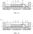
- an embodiment of the present invention provides a light sensing module Z3, which includes a substrate 1, a light sensing unit 2, a first light-transmissive component 3a, a second light-transmissive component 3b, a blocking wall 4 and a light shielding layer 5.
- the light sensing unit 2 is disposed on the substrate 1.
- the light shielding layer 5 is disposed on the substrate 1 and surrounds the light sensing unit 2.
- the first light-transmissive component 3a covers the light sensing unit 2 and the light shielding layer 5.
- the second light-transmissive component 3b is disposed between the light sensing unit 2 and the first light-transmissive component 3a.
- the blocking wall 4 is disposed on the substrate 1, and surrounds the light sensing unit 2, the first light-transmissive component 3a, the second light-transmissive component 3b and the light shielding layer 5.
- the technical details of the substrate 1, the light sensing unit 2, the first light-transmissive component 3a, the second light-transmissive component 3b and the blocking wall 4 have been described in the aforesaid examples, and will not be reiterated herein.
- the light shielding layer 5 is disposed between the light sensing unit 2 and the blocking wall 4.
- the light shielding layer 5 also has low light transmittance and can work with the blocking wall 4 to jointly realize an external light shielding function. Therefore, in the presence of the light shielding layer 5, the crosstalk of external lights on the light sensing unit 2 can be decreased. As a result, the light sensing unit 2 has a higher accuracy and can thus greatly reduce misjudgment rate.
- a lateral surface 202 of the light sensing unit 2 and the blocking wall 4 has a gap G therebetween, which can be completely or partially filled with the light shielding layer 5.
- the gap G is completely filled with the light shielding layer 5.
- the light shielding layer 5 can be formed of, for example, a resin composition including a silicone-based resin and a black carbon powder (K Black). The above-described details are merely exemplary, and are not intended to limit the present disclosure.
- a light sensing module Z4 which includes a substrate 1, a light sensing unit 2, a first light-transmissive component 3a, a second light-transmissive component 3b, a third light-transmissive component 3c, a blocking wall 4 and a light shielding layer 5.
- the light sensing unit 2 is disposed on the substrate 1.
- the light shielding layer 5 is disposed on the substrate 1 and surrounds the light sensing unit 2.
- the first light-transmissive component 3a covers the light sensing unit 2.
- the second light-transmissive component 3b is disposed between the light sensing unit 2 and the first light-transmissive component 3a.
- the third light-transmissive component 3c surrounds the first light-transmissive component 3a, and corresponds in position to the light shielding layer 5.
- the blocking wall 4 is disposed on the substrate 1, and surrounds the light sensing unit 2, the first light-transmissive component 3a, the second light-transmissive component 3b, the third light-transmissive component 3c and the light shielding layer 5.
- the technical details of the substrate 1, the light sensing unit 2, the first light-transmissive component 3a, the second light-transmissive component 3b, the blocking wall 4 and the light shielding layer 5 have been described in the aforesaid embodiments, and will not be reiterated herein.
- the first light-transmissive component 3a has a first refractive index that is between a refractive index of the light sensing unit 2 and a refractive index of air.
- the second light-transmissive component 3b has a second refractive index that is between the refractive index of the light sensing unit 2 and the first refractive index.
- the third light-transmissive component 3c has a third refractive index that is less than the first refractive index. Therefore, the first light-transmissive component 3a and the third light-transmissive component 3c can jointly realize a refractive index matching function to further increase the sensitivity of the light sensing unit 2, the related details of which are described below.
- the third light-transmissive component 3c can be a layered structure that is formed of, for example, a silicone-based resin.
- the refractive index (i.e., the third refractive index) of the third light-transmissive component 3c can be between 1.35 and 1.45, and preferably 1.4.
- the thickness of the third light-transmissive component 3c can be between 10 ⁇ m and 30 ⁇ m.
- the refractive index of the third light-transmissive component 3c is less than the refractive index of the first light-transmissive component 3a
- the working light beam L1 can undergo a total reflection at a boundary between the first light-transmissive component 3a and the third light-transmissive component 3c, so as to be received by the upper light receiving surface 201 or the lateral surface 202 of the light sensing unit 2. That is, the sensing range of the light sensing unit 2 can be increased by the refractive index matching function that is jointly realized by the first light-transmissive component 3a and the third light-transmissive component 3c.
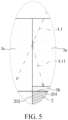
- FIG. 6 and FIG. 7 which is to be read in conjunction with FIG. 5 , another embodiment of the present invention provides a light sensing module Z5 having a structure that is the same as the structure of the light sensing module Z4 of the embodiment of FIG.4 .
- the third light-transmissive component 3c contains light diffusing particles P.
- the light diffusing particles P can result in a scattering effect of a working light beam L2, and a resulting scattered light beam L21 is able to be received by the upper light receiving surface 201 or the lateral surface 202 of the light sensing unit 2, as shown in FIG. 7 .
- the sensing range of the light sensing unit 2 can also be increased, thereby increasing sensing sensitivity.
- the light diffusing particles P can be inorganic particles, and preferably titanium dioxide particles.
- the light diffusing particles P have an average particle diameter between 10 nm and 30 nm, and are present in an amount between 0.01 wt % and 1 wt % based on 100 wt % of the third light-transmissive component 3c.
- the above-described details are merely exemplary, and are not intended to limit the present disclosure.
- the first light-transmissive component 3a can also contain light diffusing particles depending on particular implementations.
- the light sensing module Z5 of this embodiment can be manufactured by the following steps. Firstly, a substrate 1 is provided, having a first contact pad 11 and a second contact pad 12 that is separate from the first contact pad 11, and a blocking wall 4 that is formed on the substrate 1. Next, a light sensing unit 2 is attached to the first contact pad 11 of the substrate 1, and a wire W is used to connect the light sensing unit 2 to the second contact pad 12 of the substrate 1. Next, a first light-transmissive component 3a and a second light-transmissive component 3b are formed on the light sensing unit 2, in which the second light-transmissive component 3b is formed between the light sensing unit 2 and the first light-transmissive component 3a.
- a light shielding layer 5 is formed between the light sensing unit 2 and the blocking wall 4.
- a third light-transmissive component 3c with light diffusing particles P is formed on the light shielding layer 5 to surround the first light-transmissive component 3a.
- the present disclosure further provides an electronic device D, which includes a light emitting module E and a light sensing module Z1, Z2, Z3, Z4, Z5 having the structure as described above.
- the light emitting module E is configured to emit a working light beam L3.
- the light sensing module Z1, Z2, Z3, Z4, Z5 is configured to sense an intensity of the working light beam.
- the electronic device D of the present disclosure can serve as a wearable electronic device.
- the electronic device D can determine whether or not to start measuring a user's physiological signal according to the magnitude of a current generated by the light sensing unit 2.
- the light sensing module of the present disclosure in which the first light-transmissive component covers the light sensing unit and has a first refractive index that is between a refractive index of the light sensing unit and a refractive index of air, and the blocking wall is disposed on the substrate and surrounds the light sensing unit and the first light-transmissive component, has the following beneficial effects.
- the sensing range can be expanded, the blind spot can be reduced, and the crosstalk of external lights on the light sensing unit can be reduced.
- the first light-transmissive component, the combination of the first light-transmissive component and the second light-transmissive component, or the combination of the first light-transmissive component, the second light-transmissive component and the third light-transmissive component can realize a refractive index matching function individually or jointly to further increase the sensitivity of the light sensing unit.
- the light shielding layer can work with the blocking wall to jointly realize an external light shielding function. Therefore, the crosstalk of external lights on the light sensing unit can be decreased to greatly reduce misjudgment rate.
Landscapes
- Physics & Mathematics (AREA)
- General Physics & Mathematics (AREA)
- Spectroscopy & Molecular Physics (AREA)
- Engineering & Computer Science (AREA)
- General Engineering & Computer Science (AREA)
- Optics & Photonics (AREA)
- Photometry And Measurement Of Optical Pulse Characteristics (AREA)
- Led Device Packages (AREA)
Claims (14)
- Lichterfassungsmodul (Z3, Z4, Z5), welches aufweist:ein Substrat (1);eine Lichterfassungseinheit (2), die an dem Substrat (1) angeordnet ist, um eine Intensität eines Betriebslichtstrahls zu erfassen;eine erste lichtdurchlässige Komponente (3a), die die Lichterfassungseinheit (2) bedeckt, wobei die erste lichtdurchlässige Komponente (3a) einen ersten Brechungsindex hat, der zwischen einem Brechungsindex der Lichterfassungseinheit (2) und einem Brechungsindex von Luft ist; undeine Blockierwand (4), die an dem Substrat (1) angeordnet ist und die Lichterfassungseinheit (2) und die erste lichtdurchlässige Komponente (3a) umgibt;eine zweite lichtdurchlässige Komponente (3b), die zwischen der Lichterfassungseinheit (2) und der ersten lichtdurchlässigen Komponente (3a) angeordnet ist und einen zweiten Brechungsindex zwischen dem Brechungsindex der Lichterfassungseinheit (2) und dem ersten Brechungsindex hat; wobei das Lichterfassungsmodul (Z3, Z4, Z5) dadurch gekennzeichnet ist, dass es ferner aufweist:
eine Lichtschirmungsschicht (5), die zwischen der Lichterfassungseinheit (2) und der Blockierwand (4) angeordnet ist. - Lichterfassungsmodul (Z3, Z4, Z5) nach Anspruch 1, wobei die Blockierwand (4) eine Lichtdurchlässigkeit von weniger als 2 % in Bezug auf den Betriebslichtstrahl hat.
- Lichterfassungsmodul (Z3, Z4, Z5) nach Anspruch 2, wobei die Blockierwand (4) eine Dicke zwischen 50 µm und 200 µm hat.
- Lichterfassungsmodul (Z3, Z4, Z5) nach Anspruch 1, wobei die erste lichtdurchlässige Komponente (3a) eine Dicke zwischen 30 µm und 50 µm hat und die zweite lichtdurchlässige Komponente (3b) eine Dicke zwischen 10 µm und 30 µm hat.
- Lichterfassungsmodul (Z3, Z4, Z5) nach Anspruch 3 oder 4, wobei der erste Brechungsindex der ersten lichtdurchlässigen Komponente (3a) zwischen 1,45 und 1,5 ist und der zweite Brechungsindex der zweiten lichtdurchlässigen Komponente (3b) zwischen 1,54 und 1,55 ist.
- Lichterfassungsmodul (Z3) nach Anspruch 1, wobei die Lichterfassungseinheit (2) eine obere Lichtempfangsfläche (201) und eine seitliche Fläche (202), welche senkrecht zur oberen Lichtempfangsfläche (201) ist, hat, und wobei eine Lücke (G) zwischen der seitlichen Fläche (202) und der Blockierwand (4) ist, die mit der Lichtschirmungsschicht (5) gefüllt ist.
- Lichterfassungsmodul (Z3) nach Anspruch 1 oder 6, wobei die Lichtschirmungsschicht (5) eine Lichtdurchlässigkeit von weniger als 2 % in Bezug auf den Betriebslichtstrahl hat.
- Lichterfassungsmodul (Z4, Z5) nach Anspruch 1, welches ferner eine dritte lichtdurchlässige Komponente (3c) aufweist, welche die erste lichtdurchlässige Komponente (3a) umgibt und einen dritten Brechungsindex hat, der kleiner als der erste Brechungsindex ist.
- Lichterfassungsmodul (Z4, Z5) nach Anspruch 8, wobei die dritte lichtdurchlässige Komponente (3c) eine Dicke zwischen 10 µm und 30 µm hat.
- Lichterfassungsmodul (Z4, Z5) nach Anspruch 8 oder 9, wobei der dritte Brechungsindex der dritten lichtdurchlässigen Komponente (3c) zwischen 1,35 und 1,45 ist.
- Lichterfassungsmodul (Z5) nach Anspruch 8, 9 oder 10, wobei die dritte lichtdurchlässige Komponente (3c) lichtstreuende Teilchen (P) enthält.
- Lichterfassungsmodul (Z5) nach Anspruch 11, wobei die lichtstreuenden Teilchen (P) einen durchschnittlichen Teilchendurchmesser zwischen 10 nm und 30 nm haben und in einer Menge zwischen 0,01 Gew.-% und 1 Gew.-%, basierend auf 100 Gew.-% der dritten lichtdurchlässigen Komponente (3c), vorhanden sind.
- Lichterfassungsmodul (Z3, Z4, Z5) nach Anspruch 1, 2, 3, 4, 5, 6, 7, 8, 9, 10, 11 oder 12, wobei die Lichterfassungseinheit (2) eine erste Elektrode (21) an einem unteren Abschnitt davon und eine zweite Elektrode (22) an einem oberen Abschnitt davon hat, wobei das Substrat (1) eine erste Kontaktfläche (11) und eine zweite Kontaktfläche (12) hat, die voneinander getrennt sind, wobei die erste Elektrode (21) mit der ersten Kontaktfläche (11) verbunden ist und die zweite Elektrode (22) mit der zweiten Kontaktfläche (12) über einen Draht (W) elektrisch verbunden ist.
- Elektronische Vorrichtung (D), dadurch gekennzeichnet, dass sie ein lichtemittierendes Modul (E) und das Lichterfassungsmodul (Z3, Z4, Z5) nach Anspruch 1, 2, 3, 4, 5, 6, 7, 8, 9, 10, 11, 12 oder 13 aufweist, wobei das lichtemittierende Modul (E) konfiguriert ist, um einen Betriebslichtstrahl (L3) zu emittieren, und das Lichterfassungsmodul (Z3, Z4, Z5) konfiguriert ist, um eine Intensität des Betriebslichtstrahls (L3) zu erfassen.
Applications Claiming Priority (2)
| Application Number | Priority Date | Filing Date | Title |
|---|---|---|---|
| US201962935671P | 2019-11-15 | 2019-11-15 | |
| CN202011012537.1A CN112806960A (zh) | 2019-11-15 | 2020-09-23 | 光感测模块及其应用的电子装置 |
Publications (2)
| Publication Number | Publication Date |
|---|---|
| EP3823046A1 EP3823046A1 (de) | 2021-05-19 |
| EP3823046B1 true EP3823046B1 (de) | 2024-10-09 |
Family
ID=73401369
Family Applications (1)
| Application Number | Title | Priority Date | Filing Date |
|---|---|---|---|
| EP20207159.3A Active EP3823046B1 (de) | 2019-11-15 | 2020-11-12 | Lichterfassendes modul und elektronische vorrichtung mit verwendung davon |
Country Status (2)
| Country | Link |
|---|---|
| US (1) | US12072236B2 (de) |
| EP (1) | EP3823046B1 (de) |
Families Citing this family (1)
| Publication number | Priority date | Publication date | Assignee | Title |
|---|---|---|---|---|
| CN116503915B (zh) * | 2022-01-17 | 2025-06-20 | 群创光电股份有限公司 | 电子装置 |
Family Cites Families (5)
| Publication number | Priority date | Publication date | Assignee | Title |
|---|---|---|---|---|
| KR101201831B1 (ko) * | 2009-07-09 | 2012-11-15 | 제일모직주식회사 | 유-무기 하이브리드 조성물 및 이미지 센서 |
| DE102012104363A1 (de) * | 2012-05-21 | 2013-11-21 | Osram Opto Semiconductors Gmbh | Optoelektronisches Bauelement und Verfahren zu dessen Herstellung |
| US9696199B2 (en) * | 2015-02-13 | 2017-07-04 | Taiwan Biophotonic Corporation | Optical sensor |
| CA3045025A1 (en) * | 2016-12-15 | 2018-06-21 | Rhythm Diagnostic Systems, Inc. | Health monitoring systems and methods |
| CN108596096B (zh) * | 2018-04-24 | 2021-01-22 | 京东方科技集团股份有限公司 | 指纹识别装置、显示面板及其制作方法、显示装置 |
-
2020
- 2020-11-12 EP EP20207159.3A patent/EP3823046B1/de active Active
-
2023
- 2023-03-21 US US18/187,545 patent/US12072236B2/en active Active
Also Published As
| Publication number | Publication date |
|---|---|
| EP3823046A1 (de) | 2021-05-19 |
| US20230228620A1 (en) | 2023-07-20 |
| US12072236B2 (en) | 2024-08-27 |
Similar Documents
| Publication | Publication Date | Title |
|---|---|---|
| US11665310B2 (en) | Ambient light sensor windows for electronic devices comprising an optical sensor within an opening in the locally thinned area of an opaque layer | |
| US11644360B2 (en) | Light sensing module and electronic device using the same | |
| DE112018004941B4 (de) | Umgebungslichtsensoren für elektronische vorrichtungen | |
| US9891098B2 (en) | Diffuser and filter structures for light sensors | |
| CN111345013B (zh) | 一种终端 | |
| JP5715067B2 (ja) | 検出器表面 | |
| CN107480661B (zh) | 一种光学指纹传感器的光路和具有其的光学指纹传感器 | |
| US12317024B2 (en) | Electronic devices with skin sensors | |
| US10712197B2 (en) | Optical sensor package | |
| CN210199340U (zh) | 电子设备和装置 | |
| US11175700B1 (en) | Electronic devices with adjustable-appearance housing structures | |
| US10222256B2 (en) | Ambient light sensor system having light-scattering desiccant | |
| US10422876B2 (en) | Optical sensor arrangement | |
| EP3823046B1 (de) | Lichterfassendes modul und elektronische vorrichtung mit verwendung davon | |
| US10694607B1 (en) | Electronic devices with light sensor waveguides | |
| RU2765895C1 (ru) | Композитное стекло с интегрированным датчиком освещенности | |
| US12442953B2 (en) | Optical lens | |
| US20220386877A1 (en) | Proximity-temperature sensor package and earphone application | |
| EP4331475A1 (de) | Herzfrequenzdetektionsmodul und elektronische vorrichtung | |
| US20250216682A1 (en) | Electronic Device With Stray Light Redirection Structures | |
| CN119656605B (zh) | 一种具有识别压力的疼痛智能反馈系统 | |
| CN117234358B (zh) | 显示面板、显示模组及其制备方法和显示装置 | |
| EP4541276A1 (de) | Nichtinvasive blutzuckerüberwachungsvorrichtung mit verschleisspasserkennungsfunktion | |
| US20240192488A1 (en) | Electronic Device With Protected Light Sources | |
| US20240087527A1 (en) | Electronic Devices With Curved Display Surfaces |
Legal Events
| Date | Code | Title | Description |
|---|---|---|---|
| PUAI | Public reference made under article 153(3) epc to a published international application that has entered the european phase |
Free format text: ORIGINAL CODE: 0009012 |
|
| STAA | Information on the status of an ep patent application or granted ep patent |
Free format text: STATUS: THE APPLICATION HAS BEEN PUBLISHED |
|
| AK | Designated contracting states |
Kind code of ref document: A1 Designated state(s): AL AT BE BG CH CY CZ DE DK EE ES FI FR GB GR HR HU IE IS IT LI LT LU LV MC MK MT NL NO PL PT RO RS SE SI SK SM TR |
|
| STAA | Information on the status of an ep patent application or granted ep patent |
Free format text: STATUS: REQUEST FOR EXAMINATION WAS MADE |
|
| 17P | Request for examination filed |
Effective date: 20210929 |
|
| RBV | Designated contracting states (corrected) |
Designated state(s): AL AT BE BG CH CY CZ DE DK EE ES FI FR GB GR HR HU IE IS IT LI LT LU LV MC MK MT NL NO PL PT RO RS SE SI SK SM TR |
|
| GRAP | Despatch of communication of intention to grant a patent |
Free format text: ORIGINAL CODE: EPIDOSNIGR1 |
|
| STAA | Information on the status of an ep patent application or granted ep patent |
Free format text: STATUS: GRANT OF PATENT IS INTENDED |
|
| INTG | Intention to grant announced |
Effective date: 20240510 |
|
| GRAS | Grant fee paid |
Free format text: ORIGINAL CODE: EPIDOSNIGR3 |
|
| GRAA | (expected) grant |
Free format text: ORIGINAL CODE: 0009210 |
|
| STAA | Information on the status of an ep patent application or granted ep patent |
Free format text: STATUS: THE PATENT HAS BEEN GRANTED |
|
| AK | Designated contracting states |
Kind code of ref document: B1 Designated state(s): AL AT BE BG CH CY CZ DE DK EE ES FI FR GB GR HR HU IE IS IT LI LT LU LV MC MK MT NL NO PL PT RO RS SE SI SK SM TR |
|
| REG | Reference to a national code |
Ref country code: CH Ref legal event code: EP |
|
| REG | Reference to a national code |
Ref country code: DE Ref legal event code: R096 Ref document number: 602020038966 Country of ref document: DE |
|
| REG | Reference to a national code |
Ref country code: IE Ref legal event code: FG4D |
|
| REG | Reference to a national code |
Ref country code: DE Ref legal event code: R079 Ref document number: 602020038966 Country of ref document: DE Free format text: PREVIOUS MAIN CLASS: H01L0031020300 Ipc: H10F0077500000 |
|
| REG | Reference to a national code |
Ref country code: LT Ref legal event code: MG9D |
|
| REG | Reference to a national code |
Ref country code: NL Ref legal event code: MP Effective date: 20241009 |
|
| REG | Reference to a national code |
Ref country code: AT Ref legal event code: MK05 Ref document number: 1731570 Country of ref document: AT Kind code of ref document: T Effective date: 20241009 |
|
| PG25 | Lapsed in a contracting state [announced via postgrant information from national office to epo] |
Ref country code: NL Free format text: LAPSE BECAUSE OF FAILURE TO SUBMIT A TRANSLATION OF THE DESCRIPTION OR TO PAY THE FEE WITHIN THE PRESCRIBED TIME-LIMIT Effective date: 20241009 |
|
| PG25 | Lapsed in a contracting state [announced via postgrant information from national office to epo] |
Ref country code: NL Free format text: LAPSE BECAUSE OF FAILURE TO SUBMIT A TRANSLATION OF THE DESCRIPTION OR TO PAY THE FEE WITHIN THE PRESCRIBED TIME-LIMIT Effective date: 20241009 |
|
| PG25 | Lapsed in a contracting state [announced via postgrant information from national office to epo] |
Ref country code: HR Free format text: LAPSE BECAUSE OF FAILURE TO SUBMIT A TRANSLATION OF THE DESCRIPTION OR TO PAY THE FEE WITHIN THE PRESCRIBED TIME-LIMIT Effective date: 20241009 Ref country code: PT Free format text: LAPSE BECAUSE OF FAILURE TO SUBMIT A TRANSLATION OF THE DESCRIPTION OR TO PAY THE FEE WITHIN THE PRESCRIBED TIME-LIMIT Effective date: 20250210 Ref country code: IS Free format text: LAPSE BECAUSE OF FAILURE TO SUBMIT A TRANSLATION OF THE DESCRIPTION OR TO PAY THE FEE WITHIN THE PRESCRIBED TIME-LIMIT Effective date: 20250209 |
|
| PG25 | Lapsed in a contracting state [announced via postgrant information from national office to epo] |
Ref country code: FI Free format text: LAPSE BECAUSE OF FAILURE TO SUBMIT A TRANSLATION OF THE DESCRIPTION OR TO PAY THE FEE WITHIN THE PRESCRIBED TIME-LIMIT Effective date: 20241009 |
|
| PG25 | Lapsed in a contracting state [announced via postgrant information from national office to epo] |
Ref country code: BG Free format text: LAPSE BECAUSE OF FAILURE TO SUBMIT A TRANSLATION OF THE DESCRIPTION OR TO PAY THE FEE WITHIN THE PRESCRIBED TIME-LIMIT Effective date: 20241009 |
|
| PG25 | Lapsed in a contracting state [announced via postgrant information from national office to epo] |
Ref country code: ES Free format text: LAPSE BECAUSE OF FAILURE TO SUBMIT A TRANSLATION OF THE DESCRIPTION OR TO PAY THE FEE WITHIN THE PRESCRIBED TIME-LIMIT Effective date: 20241009 |
|
| PG25 | Lapsed in a contracting state [announced via postgrant information from national office to epo] |
Ref country code: NO Free format text: LAPSE BECAUSE OF FAILURE TO SUBMIT A TRANSLATION OF THE DESCRIPTION OR TO PAY THE FEE WITHIN THE PRESCRIBED TIME-LIMIT Effective date: 20250109 |
|
| PG25 | Lapsed in a contracting state [announced via postgrant information from national office to epo] |
Ref country code: LV Free format text: LAPSE BECAUSE OF FAILURE TO SUBMIT A TRANSLATION OF THE DESCRIPTION OR TO PAY THE FEE WITHIN THE PRESCRIBED TIME-LIMIT Effective date: 20241009 Ref country code: AT Free format text: LAPSE BECAUSE OF FAILURE TO SUBMIT A TRANSLATION OF THE DESCRIPTION OR TO PAY THE FEE WITHIN THE PRESCRIBED TIME-LIMIT Effective date: 20241009 Ref country code: GR Free format text: LAPSE BECAUSE OF FAILURE TO SUBMIT A TRANSLATION OF THE DESCRIPTION OR TO PAY THE FEE WITHIN THE PRESCRIBED TIME-LIMIT Effective date: 20250110 |
|
| PG25 | Lapsed in a contracting state [announced via postgrant information from national office to epo] |
Ref country code: PL Free format text: LAPSE BECAUSE OF FAILURE TO SUBMIT A TRANSLATION OF THE DESCRIPTION OR TO PAY THE FEE WITHIN THE PRESCRIBED TIME-LIMIT Effective date: 20241009 |
|
| PG25 | Lapsed in a contracting state [announced via postgrant information from national office to epo] |
Ref country code: RS Free format text: LAPSE BECAUSE OF FAILURE TO SUBMIT A TRANSLATION OF THE DESCRIPTION OR TO PAY THE FEE WITHIN THE PRESCRIBED TIME-LIMIT Effective date: 20250109 |
|
| REG | Reference to a national code |
Ref country code: CH Ref legal event code: PL |
|
| PG25 | Lapsed in a contracting state [announced via postgrant information from national office to epo] |
Ref country code: SM Free format text: LAPSE BECAUSE OF FAILURE TO SUBMIT A TRANSLATION OF THE DESCRIPTION OR TO PAY THE FEE WITHIN THE PRESCRIBED TIME-LIMIT Effective date: 20241009 |
|
| PG25 | Lapsed in a contracting state [announced via postgrant information from national office to epo] |
Ref country code: MC Free format text: LAPSE BECAUSE OF FAILURE TO SUBMIT A TRANSLATION OF THE DESCRIPTION OR TO PAY THE FEE WITHIN THE PRESCRIBED TIME-LIMIT Effective date: 20241009 |
|
| PG25 | Lapsed in a contracting state [announced via postgrant information from national office to epo] |
Ref country code: DK Free format text: LAPSE BECAUSE OF FAILURE TO SUBMIT A TRANSLATION OF THE DESCRIPTION OR TO PAY THE FEE WITHIN THE PRESCRIBED TIME-LIMIT Effective date: 20241009 |
|
| REG | Reference to a national code |
Ref country code: DE Ref legal event code: R097 Ref document number: 602020038966 Country of ref document: DE |
|
| PG25 | Lapsed in a contracting state [announced via postgrant information from national office to epo] |
Ref country code: LU Free format text: LAPSE BECAUSE OF NON-PAYMENT OF DUE FEES Effective date: 20241112 |
|
| REG | Reference to a national code |
Ref country code: CH Ref legal event code: PL |
|
| PG25 | Lapsed in a contracting state [announced via postgrant information from national office to epo] |
Ref country code: EE Free format text: LAPSE BECAUSE OF FAILURE TO SUBMIT A TRANSLATION OF THE DESCRIPTION OR TO PAY THE FEE WITHIN THE PRESCRIBED TIME-LIMIT Effective date: 20241009 |
|
| PG25 | Lapsed in a contracting state [announced via postgrant information from national office to epo] |
Ref country code: CH Free format text: LAPSE BECAUSE OF NON-PAYMENT OF DUE FEES Effective date: 20241130 |
|
| PG25 | Lapsed in a contracting state [announced via postgrant information from national office to epo] |
Ref country code: RO Free format text: LAPSE BECAUSE OF FAILURE TO SUBMIT A TRANSLATION OF THE DESCRIPTION OR TO PAY THE FEE WITHIN THE PRESCRIBED TIME-LIMIT Effective date: 20241009 |
|
| PG25 | Lapsed in a contracting state [announced via postgrant information from national office to epo] |
Ref country code: SK Free format text: LAPSE BECAUSE OF FAILURE TO SUBMIT A TRANSLATION OF THE DESCRIPTION OR TO PAY THE FEE WITHIN THE PRESCRIBED TIME-LIMIT Effective date: 20241009 |
|
| PG25 | Lapsed in a contracting state [announced via postgrant information from national office to epo] |
Ref country code: CZ Free format text: LAPSE BECAUSE OF FAILURE TO SUBMIT A TRANSLATION OF THE DESCRIPTION OR TO PAY THE FEE WITHIN THE PRESCRIBED TIME-LIMIT Effective date: 20241009 |
|
| PG25 | Lapsed in a contracting state [announced via postgrant information from national office to epo] |
Ref country code: IT Free format text: LAPSE BECAUSE OF FAILURE TO SUBMIT A TRANSLATION OF THE DESCRIPTION OR TO PAY THE FEE WITHIN THE PRESCRIBED TIME-LIMIT Effective date: 20241009 |
|
| PLBE | No opposition filed within time limit |
Free format text: ORIGINAL CODE: 0009261 |
|
| STAA | Information on the status of an ep patent application or granted ep patent |
Free format text: STATUS: NO OPPOSITION FILED WITHIN TIME LIMIT |
|
| REG | Reference to a national code |
Ref country code: BE Ref legal event code: MM Effective date: 20241130 |
|
| PG25 | Lapsed in a contracting state [announced via postgrant information from national office to epo] |
Ref country code: SE Free format text: LAPSE BECAUSE OF FAILURE TO SUBMIT A TRANSLATION OF THE DESCRIPTION OR TO PAY THE FEE WITHIN THE PRESCRIBED TIME-LIMIT Effective date: 20241009 |
|
| 26N | No opposition filed |
Effective date: 20250710 |
|
| PG25 | Lapsed in a contracting state [announced via postgrant information from national office to epo] |
Ref country code: BE Free format text: LAPSE BECAUSE OF NON-PAYMENT OF DUE FEES Effective date: 20241130 |
|
| PG25 | Lapsed in a contracting state [announced via postgrant information from national office to epo] |
Ref country code: IE Free format text: LAPSE BECAUSE OF NON-PAYMENT OF DUE FEES Effective date: 20241112 |
|
| PGFP | Annual fee paid to national office [announced via postgrant information from national office to epo] |
Ref country code: DE Payment date: 20251126 Year of fee payment: 6 |
|
| PGFP | Annual fee paid to national office [announced via postgrant information from national office to epo] |
Ref country code: GB Payment date: 20251125 Year of fee payment: 6 |
|
| PGFP | Annual fee paid to national office [announced via postgrant information from national office to epo] |
Ref country code: FR Payment date: 20251124 Year of fee payment: 6 |
|
| PG25 | Lapsed in a contracting state [announced via postgrant information from national office to epo] |
Ref country code: HU Free format text: LAPSE BECAUSE OF FAILURE TO SUBMIT A TRANSLATION OF THE DESCRIPTION OR TO PAY THE FEE WITHIN THE PRESCRIBED TIME-LIMIT; INVALID AB INITIO Effective date: 20201112 |
|
| PG25 | Lapsed in a contracting state [announced via postgrant information from national office to epo] |
Ref country code: CY Free format text: LAPSE BECAUSE OF FAILURE TO SUBMIT A TRANSLATION OF THE DESCRIPTION OR TO PAY THE FEE WITHIN THE PRESCRIBED TIME-LIMIT; INVALID AB INITIO Effective date: 20201112 |