EP3828627B1 - Elektrochromes spiegelmodul - Google Patents
Elektrochromes spiegelmodul Download PDFInfo
- Publication number
- EP3828627B1 EP3828627B1 EP20197966.3A EP20197966A EP3828627B1 EP 3828627 B1 EP3828627 B1 EP 3828627B1 EP 20197966 A EP20197966 A EP 20197966A EP 3828627 B1 EP3828627 B1 EP 3828627B1
- Authority
- EP
- European Patent Office
- Prior art keywords
- light
- electrochromic
- mirror module
- electrochromic mirror
- transmissive substrate
- Prior art date
- Legal status (The legal status is an assumption and is not a legal conclusion. Google has not performed a legal analysis and makes no representation as to the accuracy of the status listed.)
- Active
Links
Images






Classifications
-
- B—PERFORMING OPERATIONS; TRANSPORTING
- B60—VEHICLES IN GENERAL
- B60R—VEHICLES, VEHICLE FITTINGS, OR VEHICLE PARTS, NOT OTHERWISE PROVIDED FOR
- B60R1/00—Optical viewing arrangements; Real-time viewing arrangements for drivers or passengers using optical image capturing systems, e.g. cameras or video systems specially adapted for use in or on vehicles
- B60R1/02—Rear-view mirror arrangements
- B60R1/08—Rear-view mirror arrangements involving special optical features, e.g. avoiding blind spots, e.g. convex mirrors; Side-by-side associations of rear-view and other mirrors
- B60R1/083—Anti-glare mirrors, e.g. "day-night" mirrors
- B60R1/088—Anti-glare mirrors, e.g. "day-night" mirrors using a cell of electrically changeable optical characteristic, e.g. liquid-crystal or electrochromic mirrors
-
- G—PHYSICS
- G02—OPTICS
- G02F—OPTICAL DEVICES OR ARRANGEMENTS FOR THE CONTROL OF LIGHT BY MODIFICATION OF THE OPTICAL PROPERTIES OF THE MEDIA OF THE ELEMENTS INVOLVED THEREIN; NON-LINEAR OPTICS; FREQUENCY-CHANGING OF LIGHT; OPTICAL LOGIC ELEMENTS; OPTICAL ANALOGUE/DIGITAL CONVERTERS
- G02F1/00—Devices or arrangements for the control of the intensity, colour, phase, polarisation or direction of light arriving from an independent light source, e.g. switching, gating or modulating; Non-linear optics
- G02F1/01—Devices or arrangements for the control of the intensity, colour, phase, polarisation or direction of light arriving from an independent light source, e.g. switching, gating or modulating; Non-linear optics for the control of the intensity, phase, polarisation or colour
- G02F1/15—Devices or arrangements for the control of the intensity, colour, phase, polarisation or direction of light arriving from an independent light source, e.g. switching, gating or modulating; Non-linear optics for the control of the intensity, phase, polarisation or colour based on an electrochromic effect
- G02F1/153—Constructional details
- G02F1/1533—Constructional details structural features not otherwise provided for
-
- G—PHYSICS
- G02—OPTICS
- G02F—OPTICAL DEVICES OR ARRANGEMENTS FOR THE CONTROL OF LIGHT BY MODIFICATION OF THE OPTICAL PROPERTIES OF THE MEDIA OF THE ELEMENTS INVOLVED THEREIN; NON-LINEAR OPTICS; FREQUENCY-CHANGING OF LIGHT; OPTICAL LOGIC ELEMENTS; OPTICAL ANALOGUE/DIGITAL CONVERTERS
- G02F1/00—Devices or arrangements for the control of the intensity, colour, phase, polarisation or direction of light arriving from an independent light source, e.g. switching, gating or modulating; Non-linear optics
- G02F1/01—Devices or arrangements for the control of the intensity, colour, phase, polarisation or direction of light arriving from an independent light source, e.g. switching, gating or modulating; Non-linear optics for the control of the intensity, phase, polarisation or colour
- G02F1/15—Devices or arrangements for the control of the intensity, colour, phase, polarisation or direction of light arriving from an independent light source, e.g. switching, gating or modulating; Non-linear optics for the control of the intensity, phase, polarisation or colour based on an electrochromic effect
- G02F1/153—Constructional details
- G02F1/155—Electrodes
-
- G—PHYSICS
- G02—OPTICS
- G02F—OPTICAL DEVICES OR ARRANGEMENTS FOR THE CONTROL OF LIGHT BY MODIFICATION OF THE OPTICAL PROPERTIES OF THE MEDIA OF THE ELEMENTS INVOLVED THEREIN; NON-LINEAR OPTICS; FREQUENCY-CHANGING OF LIGHT; OPTICAL LOGIC ELEMENTS; OPTICAL ANALOGUE/DIGITAL CONVERTERS
- G02F1/00—Devices or arrangements for the control of the intensity, colour, phase, polarisation or direction of light arriving from an independent light source, e.g. switching, gating or modulating; Non-linear optics
- G02F1/01—Devices or arrangements for the control of the intensity, colour, phase, polarisation or direction of light arriving from an independent light source, e.g. switching, gating or modulating; Non-linear optics for the control of the intensity, phase, polarisation or colour
- G02F1/15—Devices or arrangements for the control of the intensity, colour, phase, polarisation or direction of light arriving from an independent light source, e.g. switching, gating or modulating; Non-linear optics for the control of the intensity, phase, polarisation or colour based on an electrochromic effect
- G02F1/153—Constructional details
- G02F1/157—Structural association of cells with optical devices, e.g. reflectors or illuminating devices
-
- G—PHYSICS
- G06—COMPUTING OR CALCULATING; COUNTING
- G06F—ELECTRIC DIGITAL DATA PROCESSING
- G06F3/00—Input arrangements for transferring data to be processed into a form capable of being handled by the computer; Output arrangements for transferring data from processing unit to output unit, e.g. interface arrangements
- G06F3/01—Input arrangements or combined input and output arrangements for interaction between user and computer
- G06F3/03—Arrangements for converting the position or the displacement of a member into a coded form
- G06F3/041—Digitisers, e.g. for touch screens or touch pads, characterised by the transducing means
-
- B—PERFORMING OPERATIONS; TRANSPORTING
- B60—VEHICLES IN GENERAL
- B60R—VEHICLES, VEHICLE FITTINGS, OR VEHICLE PARTS, NOT OTHERWISE PROVIDED FOR
- B60R1/00—Optical viewing arrangements; Real-time viewing arrangements for drivers or passengers using optical image capturing systems, e.g. cameras or video systems specially adapted for use in or on vehicles
- B60R1/12—Mirror assemblies combined with other articles, e.g. clocks
- B60R2001/1215—Mirror assemblies combined with other articles, e.g. clocks with information displays
-
- G—PHYSICS
- G02—OPTICS
- G02F—OPTICAL DEVICES OR ARRANGEMENTS FOR THE CONTROL OF LIGHT BY MODIFICATION OF THE OPTICAL PROPERTIES OF THE MEDIA OF THE ELEMENTS INVOLVED THEREIN; NON-LINEAR OPTICS; FREQUENCY-CHANGING OF LIGHT; OPTICAL LOGIC ELEMENTS; OPTICAL ANALOGUE/DIGITAL CONVERTERS
- G02F1/00—Devices or arrangements for the control of the intensity, colour, phase, polarisation or direction of light arriving from an independent light source, e.g. switching, gating or modulating; Non-linear optics
- G02F1/01—Devices or arrangements for the control of the intensity, colour, phase, polarisation or direction of light arriving from an independent light source, e.g. switching, gating or modulating; Non-linear optics for the control of the intensity, phase, polarisation or colour
- G02F1/13—Devices or arrangements for the control of the intensity, colour, phase, polarisation or direction of light arriving from an independent light source, e.g. switching, gating or modulating; Non-linear optics for the control of the intensity, phase, polarisation or colour based on liquid crystals, e.g. single liquid crystal display cells
- G02F1/133—Constructional arrangements; Operation of liquid crystal cells; Circuit arrangements
- G02F1/1333—Constructional arrangements; Manufacturing methods
- G02F1/13338—Input devices, e.g. touch panels
-
- G—PHYSICS
- G02—OPTICS
- G02F—OPTICAL DEVICES OR ARRANGEMENTS FOR THE CONTROL OF LIGHT BY MODIFICATION OF THE OPTICAL PROPERTIES OF THE MEDIA OF THE ELEMENTS INVOLVED THEREIN; NON-LINEAR OPTICS; FREQUENCY-CHANGING OF LIGHT; OPTICAL LOGIC ELEMENTS; OPTICAL ANALOGUE/DIGITAL CONVERTERS
- G02F2203/00—Function characteristic
- G02F2203/02—Function characteristic reflective
Definitions
- the present disclosure relates to an optical apparatus. More particularly, the present disclosure relates to an electrochromic mirror module.
- Rearview mirror with electrochromic material is utilized in vehicles nowadays.
- the electrochromic material can provide a rearview with higher brightness during the day to observe rear vehicles, and increase the light absorption at night to provide an anti-glare function, so as to avoid that the lights of the rear vehicles affect driver's vision.
- switch and adjusting buttons of the electrochromic rearview mirror are located on the bottom, which are hard to reach. Some of the electrochromic rearview mirror has switch and buttons located on the reflective surface, which are blocking the rearview vision of the driver. Therefore, how to provide an electrochromic rearview mirror with an appropriate control interface is one of the problems to be solved by people skilled in the art.
- US 9 346 403 B2 refers to a rearview assembly comprising a first light-transmissive front substrate having a visible front surface and a rear surface disposed opposite to the visible surface; an opaque touch sensing layer being disposed on the rear surface; and an electrochromic device in the form of a reflective element being disposed on the rear surface with the opaque touch sensing layer, wherein, on the rear surface, an user input area where the opaque touch sensing layer is disposed and an area where the electrochromic device is disposed are different so that the user input area is substantially devoid of metallic and/or conductive coatings such that the conductive coatings of the mirror reflective element are not at the user input area and do not interfere with the touch sensor.
- US 2017 297 498 A1 refers to an interior rearview mirror comprising an electrochromic mirror module in the form of an electro-optic mirror reflective element comprising a first light-transmissive front glass having a visible front surface and a rear surface disposed opposite to the visible surface; an capacitive touch sensor being disposed on the rear surface; where said electro-optic mirror reflective element includes a front substrate and a rear substrate spaced from the front substrate with an electrochromic medium and transparent, conductive or semi-conductive layers sandwiched between the substrates with the transparent conductive layer disposed at a rear surface of the front substrate and the transparent conductive layer disposed at the front surface of the rear substrate, wherein, on the back surface, an area where the opaque touch sensing layer is disposed and an area where the electrochromic device is disposed are different.
- US 2014 022 390 A1 refers to a mirror reflective element assembly comprising a first light-transmissive substrate having a visible surface and a back surface disposed opposite to the visible surface; an opaque touch sensing layer being disposed on the back surface; and an electrochromic device being disposed on the back surface with the opaque touch sensing layer, wherein, on the back surface, an area where the opaque touch sensing layer is disposed and an area where the electrochromic device is disposed are different.
- An embodiment of the present invention provides an electrochromic mirror module according to appended independent claim 1.
- An electrochromic mirror module of an embodiment of the present disclosure can be applied to a vehicle.
- an electrochromic mirror module of an embodiment of the present disclosure can be applied to rear-view mirror inside a car or rear-view mirrors on the external of the car, and the electrochromic mirror can also apply to rear-view mirror of other vehicles such as a scooter, or an electrical bicycle, but the disclosure is not limited thereto.
- the technical words “the first”, “the second”, “the third” and etc. in the text can be used to describe different devices, components, areas, layers and/or parts, but the devices, components, areas, layers and/or parts should not be limited by these technical words.
- the technical words are used to differentiate one device, component, area, layer and/or part from others.
- “the first device”, “the component,” “the area,” “the layer” and/or “the part” can also be called “the second device”, “the component,” “the area,” “the layer” and/or “the part” without departing from the teaching herein.
- Fig. 1 is a schematic perspective view of an electrochromic mirror module of an embodiment of the present disclosure.
- the electrochromic mirror module 100 of the embodiment of the present disclosure can provide a visible surface 101.
- the electrochromic mirror module 100 can be installed to a car, and a driver can see rearward through the visible surface 101.
- the electrochromic mirror module 100 of the embodiment may include a connecting end 102, and the electrochromic mirror module 100 can be installed on a windshield of a car through the connecting end 102, but the present disclosure is not limited thereto.
- the connecting end 102 can be attached to the windshield through, for instance, adhesive, or external knob being able to couple with a fixing trench on the windshield, but the present disclosure is not limited thereto.
- the connecting end 102 can include, for instance, a shaft disposed on the side connecting to the windshield or the side connecting the electrochromic mirror module 100, and the shaft can be, for instance, a ball shaft, but the present disclosure is not limited thereto.
- the present disclosure is not limited to shape and quantity of the connecting end, and people skilled in the art can modify the number and the shape of the connecting end 102 according to demand, so as to connect the electrochromic mirror module 100 to a windshield of car properly.
- the electrochromic mirror module 100 of the present disclosure can include, for instance, a case 103.
- the case 103 of the present disclosure can wrap part of the electrochromic mirror module 100 located at the back of the visible surface 101.
- the electrochromic mirror module 100 of the present disclosure can provide the visible surface 101 that is frameless, but the present disclosure is not limited thereto.
- an electrochromic mirror module 100 can provide a framed visible surface 101.
- a material of the case 103 may include acrylic with higher hardness, or other materials which is adapted to support, but the present disclosure is not limited thereto.
- the present disclosure is not limited to the shapes, size, and the case 103 and the connection of the connecting end 102, and the following will further describe the detailed elements of the electrochromic mirror module 100.
- Fig. 2 is a sectional view taken along the cutting plane line I in Fig. 1 .
- the thickness of layers, films, panels, regions, etc. are exaggerated for clarity.
- the same reference numerals denote the same component. It will be understood that when a component such as a layer, a film, a region or a substrate is referred to as “on” or “connected to” another component, intermediate components can also be present. In contrast, when a component is referred to as “directly on” or “directly connected to” another component, no intermediate component can be present.
- “connected” may refer to both physical and/or electrical connections.
- electrical connection or “coupled” may be the presence of other components between two elements.
- the electrochromic mirror module 100 includes a first light-transmissive substrate 110, an opaque touch sensing layer 120, and a electrochromic device 130.
- the first light-transmissive substrate 110 has a visible surface 101 and a back surface 111 disposed opposite to the visible surface 101.
- the opaque touch sensing layer 120 and the electrochromic device 130 are disposed on the back surface 111 of the first light-transmissive substrate 110.
- the opaque touch sensing layer 120 and the electrochromic device 130 are disposed on different areas of the back surface 111.
- distribution area of the opaque touch sensing layer 120 on the back surface 111 is corresponded to the peripheral of the visible surface 101, and the rest of the visible surface 101 is corresponded to the electrochromic device 130.
- Peripheral of the said visible surface 101 includes, for instance, edge or corner areas of the visible surface 101, and the electrochromic device 130 can provide reflection image with high brightness or reflection image with low brightness.
- the electrochromic mirror module 100 of the embodiment can be a rearview mirror of a car, and the electrochromic mirror module 100 can provide touch function on the visible surface 101 with the opaque touch sensing layer 120, and a driver can control the electrochromic device 130 or other devices on the visible surface 101. Also, the driver can see rearward through the other area of the visible surface 101 with the electrochromic device 130.
- the visible surface 101 of the electrochromic mirror module 100 of the embodiment can be a plane, but the disclosure is not limited thereto. In other embodiments, the visible surface 101 of the electrochromic mirror module 100 can be plane or curved surface. In other embodiments of the present disclosure, the visible surface 101 of the electrochromic mirror module 100 can be a 2.5D surface. Moreover, a shape of the visible surface 101 is rectangle, but the disclosure is not limited thereto. In other embodiments of the present disclosure, shape of the visible surface 101 of the electrochromic mirror module 100 can be round, oval, or polygonal. Furthermore, peripheral of the visible surface 101 of the embodiment has right angle, but the disclosure is not limited thereto. In other embodiments, the peripheral of the visible surface 101 may have right angle, round angle (r angle), or 2.5D angle.
- the visible surface 101 of the present disclosure has a viewing area A and a operation area B.
- the operation area B is distributed at the peripheral of the visible surface 101, and the viewing area A covers center of the visible surface 101.
- projection area of the opaque touch sensing layer 120 on the visible surface 101 is located in the operation area B, and projection area of the electrochromic device 130 on the visible surface 101 at least overlap the viewing area A.
- the viewing area A and the operation area B on the visible surface 101 of the electrochromic mirror module 100 are separate, and, therefore; viewing area A won't be block while the driver is touching the operation area B, and driving safety can be further improved.
- visible surface 101 on the first light-transmissive substrate 110 of the embodiment can provide viewing and operation functions at the same time, and the case 103 of the electrochromic mirror module 100 can connect to the back surface 111 of the first light-transmissive substrate 110, and the electrochromic mirror module 100 can provide the visible surface 101 that is frameless, and visible experience of the driver can be improved, but the disclosure is not limited thereto.
- the case 103 can provide a side wall surrounding the first light-transmissive substrate 110, and the side wall can has a front casing surface which is aligned with the visible surface 101, and the surface of the electrochromic mirror module 100 facing the driver can be a full flat surface.
- the visible surface 101 of the embodiment is rectangle, includes top L1, bottom L2, and two sides L3, L4.
- a length of the top L1 and a length of the bottom L2 are longer than lengths of the two sides L3, L4.
- distribution area of the opaque touch sensing layer 120 on the back surface 111 corresponds to an area on the visible surface 101 near the bottom L2.
- the area corresponded to the opaque touch sensing layer 120 is located at the lower side of the visible surface 101, and an area of the visible surface 101 corresponded to the electrochromic device 130 will not be block by the driver's hands during operation.
- the area on the visible surface 101 that is corresponded to the opaque touch sensing layer 120 has a width W1 on a direction perpendicular to the bottom L2, and the width can be 6 millimeters (mm), but the disclosure is not limited thereto.
- the area on the visible surface 101 corresponded to the opaque touch sensing layer 120 has a width W1 on a direction perpendicular to the bottom L2, and the width W1 is ranged from 6 mm to 10 mm.
- the width W1 can be further increased as required. Therefore, the opaque touch sensing layer 120 can provide a good sensing area, without occupying too much area on the visible surface 101.
- a material of the first light-transmissive substrate 110 can include glass, but the disclosure is not limited thereto.
- the material of the first light-transmissive substrate 110 can include light-transmissive acrylic, and the material of the first light-transmissive substrate 110 can also include a material absorbing light in specific spectrum, but the disclosure is not limited thereto.
- the opaque touch sensing layer 120 forms capacitors on the first light-transmissive substrate 110, and sensing signals can be generated while the driver's hand is touching the visible surface 101.
- the electrochromic mirror module 100 of the embodiment can include a processor, and the processor is electrically connected to the opaque touch sensing layer 120, and the opaque touch sensing layer 120 can generate sensing signals according to the area where the driver touch through mutual capacitance or self-capacitance, but the disclosure is not limited thereto.
- the opaque touch sensing layer 120 can include patterned metal electrodes 121, and the patterned metal electrodes 121 are disposed on the back surface 111 of the first light-transmissive substrate 110, and the patterned metal electrodes 121 has hollow areas C, and the patterned metal electrodes 121 form a plurality of electrode patterns 122 ⁇ 127 as shown in Fig. 1 though the shape of hollow areas C.
- Fig. 1 Please refer to Fig. 1 .
- the patterned metal electrodes 121 can be form into the electrode patterns 122 ⁇ 127, while the electrode pattern 127 may correspond to, for instance, power of the electrochromic device 130, and the electrode pattern 126 may correspond to the GPS (global positioning system) function of the car, and the electrode pattern 125 may correspond to wireless transfer function, and the electrode pattern 124 may correspond to hands-free calling, and the electrode pattern 123 may correspond to brightness adjustment, and the electrode pattern 122 may correspond to reset.
- the electrochromic mirror module 100 can further electrically connect to a controller of the car, and controlling the mobile phone, wireless transferring module, or GPS through the touch function of the opaque touch sensing layer 120.
- the driver can control the electrochromic device 130 of the electrochromic mirror module 100 of the embodiment through the opaque touch sensing layer 120, and the driver can control other function of the car through this interface.
- the opaque touch sensing layer 120 of the embodiment of the disclosure can provide an easy and low-cost manufacturing method.
- the patterned metal electrode 121 of the embodiment and its connecting circuit can be form on the back surface 111 of the first light-transmissive substrate 110 through coating.
- the patterned metal electrodes 121 and its connecting circuit can be form on the back surface 111 of the first light-transmissive substrate 110 through one photolithography process.
- Formation of the patterned metal electrodes 121 may include: forming a metal layer on the back surface 111 of the first light-transmissive substrate 110 through chemical vapor deposition or physical vapor deposition; pattering the metal layer through a photolithography with a mask, and forming hollow areas C in part of the metal layer.
- the hollow area C can further divide or cut the metal electrode into a plurality of separate touch operation areas, and forming the patterns according to every touch operation areas, so as to form a plurality of buttons and connection circuits thereof.
- buttons and the connection circuits of the opaque touch sensing layer 120 can be formed through one photolithography process. Therefore, the opaque touch sensing layer 120 can provide a proper control interface and a low cost manufacture method, and the total cost of the manufacture of the electrochromic mirror module 100 may also be reduced. Moreover, size, width, and position of the opaque touch sensing layer 120 may also be modified easily, and customization of the electrochromic mirror module 100 will be easier.
- a material of the patterned metal electrode 121 can include aluminum, but the disclosure is not limited thereto.
- the material of the patterned metal electrode 121 can include silver, gold, copper, titanium, molybdenum, chromium, nickel, platinum, or complex material consisting thereof.
- the formation of the patterned metal electrode 121 on the back surface 111 of the first light-transmissive substrate 110 includes coating or printing.
- the visible surface 101 can be a full mirror surface.
- the electrode patterns 122 ⁇ 127 are arranged at the bottom side L2 of the visible surface 101, but the disclosure is not limited thereto. In other embodiment, the electrode patterns 122 ⁇ 127 can be arranged at the top side L1 of the visible surface 101.
- the electrochromic mirror module has an adhesive layer 140.
- the adhesive layer 140 and the opaque touch sensing layer 120 are both disposed between the first light-transmissive substrate 110 and the electrochromic device 130, and, therefore; the electrochromic device 130 can be bond to the first light-transmissive substrate 110.
- the electrochromic device 130 has a first controlling electrode 132, electrochromic layer 133 and a second controlling electrode 134.
- the electrochromic layer 133 is disposed between the first controlling electrode 132 and the second controlling electrode 134.
- Distance between the first controlling electrode 132 and the first light-transmissive substrate 110 is shorter than distance between the second controlling electrode 134 and the first light-transmissive substrate 110.
- the first controlling electrode 132 and the second controlling electrode 134 of the embodiment may include light-transmissive conductive material.
- the light-transmissive conductive material may include indium tin oxide, indium zinc oxide, aluminum tin oxide, aluminum zinc oxide, indium gallium zinc oxide, or fluorine doped tin oxide, or complex material consists thereof.
- the electrochromic mirror module 100 apply voltage between the first controlling electrode 132 and the second controlling electrode 134, so as to form an electric field on the electrochromic layer 133.
- the electrochromic layer 133 has electrochromic material, and optical properties (reflectance, transmittance, or absorbance and etc.) can varied with the electric field in stable, reversible manners. Therefore, the first controlling electrode 132 and the second controlling electrode 134 can control the optical properties of the electrochromic layer 133.
- the electrochromic layer 133 has reflectance that is larger than 40% corresponded to the incident light i1. In other embodiments, the reflectance of the electrochromic mirror module 100 resulting from the electrochromic layer 133 and the reflective substrate 135 is larger than 40% corresponded to the incident light i1.
- the electrochromic layer 133 has transmittance that is larger than 15% corresponded to the incident light i1.
- material of the electrochromic layer 133 of the embodiment is organic material.
- the organic material may be polymer such as EDOT, Viologen, or PMMA.
- the electrochromic layer 133 is self-illuminating material.
- first controlling electrode 132, and the second controlling electrode 134 may include material chooses from indium tin oxide, indium zinc oxide, aluminum tin oxide, aluminum zinc oxide, indium gallium zinc oxide, or fluorine doped tin oxide, or complex material consists thereof.
- the electrochromic device 130 includes second light-transmissive substrate 131 and reflective substrate 135, and the reflective substrate 135 is corresponded to the second light-transmissive substrate 131. Distance between the second light-transmissive substrate 131 and visible surface 101 is shorter than distance between the reflective substrate 135 and visible surface 101.
- the first controlling electrode 132 is disposed on the surface of the second light-transmissive substrate 131 facing towards the electrochromic layer 133, and the second controlling electrode 134 is disposed on surface of the reflective substrate 135 facing towards the electrochromic layer 133.
- the incident light i1 can reach the electrochromic layer 133 through the second light-transmissive substrate 131, and the light passes through the electrochromic layer 133 can be reflected by the reflective substrate 135, so as to provide reflected light i2 with the electrochromic device 130.
- the second light-transmissive substrate 131 may be glass substrate, and the reflective substrate 135 may be metal substrate or non-metallic substrate or glass substrate coated with metal, so as to provide a reflective surface.
- the reflective substrate 135 may also be a reflective layer, and material of the reflective layer may include coating material.
- the coating material may include silver, copper, aluminum, titanium, molybdenum, or alloy combined with one or plurality of the materials above. The present disclosure is not limited to the material of the reflective substrate 135.
- the electrochromic layer 133 can lower the absorbance or increase reflectance by controlling electric field between the first controlling electrode 132 and the second controlling electrode 134, so as to increase the brightness of the reflected light i2, and the driver can clearly observe rear view of the vehicle.
- the electrochromic layer 133 can increase the absorbance and lower the reflectance by controlling electric field between the first controlling electrode 132 and the second controlling electrode 134, so as to reduce the brightness of the reflected light i2, and the driver can avoid glare from lights behind the vehicle, which may cause annoyance, discomfort, or vision damage.
- the electrochromic mirror module 100 can further include a carrier substrate 150, and the electrochromic device 130, the opaque touch sensing layer 120, and the first light-transmissive substrate 110 are disposed on the carrier substrate 150 along the direction d1 in series.
- the carrier substrate 150 may also be glass substrate or metal substrate, so as to provide proper support, but the disclosure is not limited thereto.
- the electrochromic mirror module can further include color layer.
- Fig. 3 is a sectional view of the electrochromic mirror module of another embodiment of the present disclosure. Please refer to Fig. 3 , the electrochromic mirror module 100A is similar to the electrochromic mirror module 100 above, and descriptions of the same component will not be repeated.
- the electrochromic mirror module 100A further includes color layer 160.
- the patterned metal electrode 121 of the opaque touch sensing layer 120 is disposed between the color layer 160 and the first light-transmissive substrate 110.
- color of the color layer 160 may be white, and part of the color layer 160 may be visible in hollow area C of the patterned metal electrode 121.
- Driver may see white color in hollow area C of the patterned metal electrode 121 through the visible surface 101 of the first light-transmissive substrate 110, and the shape of the patterned metal electrode 121 may be even more visible.
- color layer 160 of the electrochromic mirror module 100A may include light-emitting device.
- the light-emitting device may be light emitting diode (LED), but the disclosure is not limited thereto.
- the light-emitting device of the color layer 160 located behind the patterned metal electrode 121 may provide backlight, and the light can reach the visible surface 101 through the hollow area C, and, therefore; shape of the patterned metal electrode 121 can be readable in dark environment.
- light-emitting device of the color layer 160 can provide different light in different position, so that the driver can more clearly recognize the shape of the patterned metal electrode.
- material of the patterned metal electrode 121 may include conductive material or coating material.
- the coating material may include silver, copper, titanium, molybdenum, aluminum, or alloy combined with one or plurality of the materials above.
- Fig. 4 is plan view of the electrochromic mirror module 100B of still another embodiment of the present disclosure. Please refer to Fig. 4 , the electrochromic mirror module 100B is similar to the electrochromic mirror module 100 above, and descriptions of the same components will not be repeated. Distribution areas of the opaque touch sensing layer 120 on the back surface are corresponded to areas near two sides L3, L4 of the visible surface 101.
- the position on the visible surface 101 being corresponded to the opaque touch sensing layer 120 forming the electrode patterns 122 ⁇ 127 can be adjacent to the side L4, the bottom L2, and the side L3 far away from the driver.
- the electrode pattern 123 ⁇ 127 which may be reachable can be locate adjacent to the side L4 or the bottom L2, and the electrode pattern 122 that should be avoided by accidental activation can be located adjacent to side L3.
- Fig. 5 is plan view of electrochromic mirror module of yet another embodiment. Please refer to Fig. 5 , the electrochromic mirror module 100C is similar to the electrochromic mirror module 100B above, and descriptions of the same components will not be repeated. Distribution areas of the opaque touch sensing layer 120 on the back surface are corresponded to areas near top L1 of the visible surface 101.
- the electrode patterns 122 ⁇ 127 of the opaque touch sensing layer 120 can corresponded to area of the visible surface 101 that is adjacent to the top L1, which is far from driver. Therefore, operation may be further avoid during driving.
- corresponded area of electrode pattern 124 for phone calls and electrode pattern 125 for wireless transmitting can be adjacent to the top L1, reminding the driver not to use these functions during driving, so as to improve safety.
- the electrode patterns 122 ⁇ 127 are spaced with different distance on the top L1, bottom L2, and the sides L3, L4 of the visible surface 101, but the disclosure is not limited thereto. In other embodiment, the electrode patterns 122 ⁇ 127 may be spaced with the same distance on the top L1, bottom L2, and the sides L3, L4 of the visible surface 101.
- Fig. 6 is a plan view of an electrochromic mirror module of another embodiment of the present disclosure.
- opaque touch sensing layer 120D of the electrochromic mirror module 100D has a continuous operation area.
- the opaque touch sensing layer 120D may further include patterned metal electrode 121, which is patterned with hollow areas D.
- the opaque touch sensing layer 120D has a continuous operation area, so as to provide an easy operation for driver.
- Fig. 7 is a plan view of the electrochromic mirror module of still another embodiment of the present disclosure.
- the opaque touch sensing layer 120E has separate operation areas 128, which are gapped with hollow areas E.
- the opaque touch sensing layer 120E has a plurality of patterned metal electrode 121, which are disposed in the operation areas 128 respectively.
- the opaque touch sensing layer 120E further includes connecting circuits 129 electrically connected to the patterned metal electrodes 121, the patterned metal electrode 121 are electrically connected to inner parts of the electrochromic mirror module 100E or processor 170 in vehicle, so as to process the touch signal from the electrochromic mirror module 100E through the processor 170.
- the connecting circuits 129 are shown enlarged for ease of explanation, but it's not to limit the position or size of the connecting circuits 129 of the embodiment, and the connecting circuits will be omitted in other figures to clearly illustrate other components of other embodiments.
- Fig. 8 is plan view of electrochromic mirror module of yet another embodiment.
- patterned metal electrodes 121 of opaque touch sensing layer 120F of the electrochromic mirror module 100F are disposed on the right side of the visible surface 101, and hollow areas F are located among the patterned metal electrodes 121, so as to provide a separate operation areas with the opaque touch sensing layer 120F.
- the patterned metal electrodes 121 can be disposed on the left of the visible surface, but the present disclosure is not limited thereto.
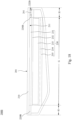
- Figs. 9-11 are section view of the first light-transmissive substrate of other embodiments.
- edge of the visible surface 101 has right angle, but the present disclosure is not limited thereto.
- edge connecting visible surface 101 and back surface 111 of first light-transmissive substrate 110A forms round angle R1 at a side near the visible surface 101, and the back surface 111 is disposed opposite to the visible surface 101.
- edge connecting visible surface 101 and back surface 111 of the first light-transmissive substrate 110B form round angle R2 at a side near the back surface 111, and the back surface 111 is disposed opposite to the visible surface 101.
- distance between the visible surface 101 and the back surface 111 can be reduced towards the bottom L2, and the back surface 111 is disposed opposite to the visible surface 101, and round angle R3 can be form at the top L1 with the visible surface 101 and the back surface 111.
- an electrochromic mirror module of an embodiment of the present disclosure can provide a operable interface on periphery of a visible surface with an opaque touch sensing layer, and the manufacture of the module is easy, and an observation area is provided at area in the visible surface corresponded to the electrochromic device, and the observation area won't be affected by operation area at periphery of the visible surface.
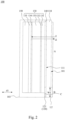
- Fig. 12 is a plan view of an electrochromic mirror module 200 of an embodiment of the present disclosure, and components below the first light-transmissive substrate 210 are illustrated with solid lines.
- Fig. 13 is a sectional view taken along the cutting plan line II in Fig. 12 . Please refer to Fig. 12 , and Fig. 13 , the electrochromic mirror module 200 has a first light-transmissive substrate 210, reflective layer 220, electrochromic device 230 and a first light-emitting device 240.
- the first light-transmissive substrate 210 has a visible surface 201 and a back surface 211.
- the back surface 211 is disposed opposite to the visible surface 201, and the visible surface 201 is facing towards the outside of the electrochromic mirror module 200, and the back surface 211 is located opposite to the visible surface 201, which is the opposite side of the first light-transmissive substrate 210, and the back surface 211 is facing towards the inner parts of the electrochromic mirror module 200.
- the back surface 211 has a first area G (illustrated with dash in Fig. 12 ) and second area H.
- Reflective layer 220 is disposed on the second area H of the back surface 211.
- Reflective layer 200 has first openings 221.
- the electrochromic device 230 is disposed on the first area G of the back surface 211.
- the first light-emitting device 240 is disposed at the first openings 221 of the reflective layer 220.
- the reflective layer 220, the electrochromic device 230 and the first light-emitting device 240 are located at the same side of the first light-transmissive substrate 210, and the reflective layer 220, the electrochromic device 230, and the first light-emitting device 240 are adjacent to the back surface 211 of the first light-transmissive substrate 210.
- Light from the first light-emitting device 240 can reach the first light-transmissive substrate 210 through the first openings 221 of the reflective layer 220, and emits through visible surface 201 of the first light-transmissive substrate 210.
- the first light-emitting device 240 is disposed at the first openings 221 of the reflective layer 220, and the reflective layer 220 and the electrochromic device 230 are disposed on different areas of the back surface 211 of the first light-transmissive substrate 210, and, therefore; the light from the first light-emitting device 240 won't affect the electrochromic device 230, and provides a proper image to driver.
- material of the reflective layer 220 has silver, but the disclosure is not limited thereto.
- the reflective layer 220 may include coating material.
- the coating material may include silver, copper, titanium, molybdenum, aluminum, or alloy combined with one or plurality of the materials above.
- the reflective layer 220 is disposed on the back surface 211 of the first light-transmissive substrate 210 through coating, but the disclosure is not limited thereto. In other embodiments, the reflective layer 220 can be disposed to the back surface 211 of the first light-transmissive substrate 210 through lamination, printing, or deposition.
- the electrochromic mirror module 200 may include a plurality of first light-emitting devices 240, and the first light-emitting devices 240 can be arranged in each of the first openings 221.
- the first light-emitting devices 240 are arranged in the first opening 221, and light from the first light-emitting devices 240 can form an illuminating pattern on the visible surface 201.
- the electrochromic mirror module 200 of the embodiment can be disposed on the outside of the vehicle, and the electrochromic mirror module 200 is disposed in the vision of driver.
- the first light-emitting devices 240 emit light and form a turning pattern on the visible surface 201. Therefore, the electrochromic mirror module 200 can provide turn signal.
- the second area H of the back surface 211 is corresponded to the peripheral of the visible surface 201.
- the first area G of the back surface 211 is corresponded to the rest of the visible surface 201.
- the second area H of the back surface 211 of the embodiment surrounds the first area G.
- the first openings 221 are formed in the second area H of the reflective layer 220, and the position of the first light-emitting device 240 won't be affected by the electrochromic device 230 in driver's vision.
- the visible surface 201 is a full mirror surface.
- the electrochromic mirror module 200 of the embodiment may further include a case 202.
- the case 202 is connected to the back surface 211 of the first light-transmissive substrate 210.
- the case 202 has an accommodation space 203, and the accommodation space 203 accommodates the electrochromic device 230 and the first light-emitting device 240.
- the accommodation space 203 is located between the case 202 and the first light-transmissive substrate 210, and connecting position of the case 202 on the first light-transmissive substrate 210 doesn't exceed distribution area of the back surface 211.
- visible surface 201 of the electrochromic mirror module 200 is a flat surface, but the present disclosure is not limited thereto. In other embodiments, visible surface 201 of the electrochromic mirror module 200 can be curved.
- the electrochromic device 230 has a second light-transmissive substrate 231, a first controlling electrode 232, an electrochromic layer 233, a second controlling electrode 234, and a rear substrate 235.
- the second light-transmissive substrate 231 is adjacent to the first light-transmissive substrate 210, and the first controlling electrode 232 is disposed on the second light-transmissive substrate 231.
- the first controlling electrode 232 may be light-transmissive electrode.
- material of the first controlling electrode 232 may include indium tin oxide, but the disclosure is not limited thereto. In other embodiments, material of the first controlling electrode 232 can include indium tin oxide, indium zinc oxide, aluminum tin oxide, aluminum zinc oxide, indium gallium zinc oxide, or fluorine doped tin oxide, or complex material consists thereof.
- the electrochromic layer 233 is disposed between the first controlling electrode 232 and the second controlling electrode 234.
- the electrochromic mirror module 200 can apply voltage to the first controlling electrode 232 and the second controlling electrode 234, so as to form an electric field on the electrochromic layer 233, and the transmittance of the electrochromic layer 233 can be adjust.
- the electrochromic layer 233 is located between the second light-transmissive substrate 231 and the rear substrate 235.
- the second controlling electrode 234 is disposed on the rear substrate 235, and the second controlling electrode 234 is a reflective electrode.
- material of the second controlling electrode 234 may include metal.
- materials of the second light-transmissive substrate 231 and the rear substrate 235 may include glass or plastic, but the disclosure is not limited thereto.
- the electrochromic mirror module 200 can apply voltage on the first controlling electrode 232 and the second controlling electrode 234, so as to control the light transmittance of the electrochromic device 230.
- the electrochromic mirror module 200 has an adhesive layer 250.
- the adhesive layer 250 is disposed between the first light-transmissive substrate 210 and the electrochromic device 230, and the adhesive layer 250 connects the electrochromic device 230 to the first light-transmissive substrate 210.
- the adhesive layer 250 and the reflective layer 220 are both disposed on the back surface 211 of the first light-transmissive substrate 210.
- the adhesive layer 250 is disposed in the first area G of the back surface 211, and the reflective layer 220 is disposed in the second area H of the back surface 211.
- the reflective layer 220 and the adhesive layer 250 may be located at different position on the first light-transmissive substrate 210.
- Fig. 14 is a block diagram of an electrochromic mirror module 200 of an embodiment of the present disclosure.
- the electrochromic mirror module 200 has the electrochromic device 230 and a first light-emitting device 240.
- the first light-emitting device 240 is electrically connected to first processor 51.
- the first light-emitting device 240 is adapted to receive a turn signal from the first processor 51.
- the first processor 51 can be central processing unit (CPU) or engine control unit (ECU) of a vehicle.
- CPU central processing unit
- ECU engine control unit
- the first processor 51 can turn on the blinker 54 and provide a turn signal 52 to the first light-emitting device 240, and turning indicator of the vehicle 50 may be enhanced.
- the first processor 51 can electrically connected to the electrochromic device 230, and the vehicle 50 may also control the optical properties of the electrochromic device 230.
- Fig. 15 is a sectional view of an electrochromic mirror module of another embodiment of the present disclosure. Please refer to Fig. 15 , the electrochromic mirror module 200A is similar to the electrochromic mirror module 200 of the embodiment above, and descriptions of the same components will not be repeated.
- the electrochromic mirror module 200A has a reflective layer 220A and sensor 260, which is different from the electrochromic mirror module 200.
- the reflective layer 220A has second opening 222.
- the sensor 260 is disposed in the second opening 222.
- the senor 260 can be a radar obstacle detector, but the present disclosure is not limited thereto. In other embodiments, the sensor 260 can be an image sensor.
- the sensor 260 of the embodiment can provide image-capturing function or obstacle detection.
- the sensor 260 may function as a dash camera without blocking the electrochromic device 230.
- the electrochromic mirror module 200A of the present disclosure may have a second light-emitting device 241, and the reflective layer 220A may have third opening 223.
- the second light-emitting device 241 is disposed in the third opening 223.
- Fig. 16 is a block diagram of an electrochromic mirror module 200A of another embodiment of the present disclosure.
- the electrochromic mirror module 200A may have a second processor 270.
- the second processor 270 is electrically connected to the sensor 260 and the second light-emitting device 241.
- the second processor 270 is adapted to receive an alert signal 262 from the sensor 260, and the second processor 270 can provide a lighting signal 271 to the second light-emitting device 241 corresponding to the alert signal 262.
- the electrochromic device 230 helps the driver see areas behind the vehicle, and the sensor 260 can provide blind spot detection.
- the second light-emitting device 241 will light up to inform the driver, and provide a safer driving environment.
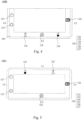
- Fig. 17 is a schematic plan view of an electrochromic mirror module of still another embodiment of the present disclosure, while components below the outer surface area illustrated with dash.
- Fig. 18 is a sectional view of the electrochromic mirror module taken along cutting plan line III in Fig. 17 .
- Fig. 19 is a sectional view of the electrochromic mirror module taken along cutting plan line IV.
- Fig. 20 is a sectional view of the electrochromic mirror module taken along cutting plan line V.
- the electrochromic mirror module 200B is similar to the electrochromic mirror module 200 of the embodiment above, and descriptions of the same components will not be repeated.
- the electrochromic mirror module 200B has first light-transmissive substrate 210, electrochromic device 230, and adhesive layer 250.
- the first light-transmissive substrate 210 has a visible surface 201 and a back surface 211.
- the electrochromic device 230 has a second light-transmissive substrate 231, first controlling electrode 232, electrochromic layer 233, second controlling electrode 234, and rear substrate 235.
- the electrochromic mirror module 200B has reflective layer 220B, sensor 260, and sensor 261, which is different from the electrochromic mirror module 200.
- the electrochromic device 230 is disposed in the first area G of the back surface 211, and the reflective layer 220B is disposed in the second area H of the back surface 211.
- the reflective layer 220B has second opening 222A and second opening 222B , and the sensor 260 is disposed in the second opening 222A , and the sensor 261 is disposed in the second opening 222B.
- the reflective layer 220B has a plurality of first openings 221 and a plurality of second openings 222A.
- the first openings 221 are adjacent to top 210A and bottom 210C of the first light-transmissive substrate 210.
- the first light-emitting device 240 are disposed in the first openings 221, and multiple first light-emitting device 240 can be arranged in each of the first openings 221.
- the second openings 222A and the second openings 222B are adjacent to side 210B of the first light-transmissive substrate 210.
- the electrochromic mirror module 200B has a plurality of sensors 260, and each of the sensors 260 may have a radar obstacle detector. Since the sensors 260 are disposed on the second openings 222A respectively, the electrochromic mirror module 200B can provide blind spot detection.
- the electrochromic mirror module 200B can have second light-emitting device 241, and the reflective layer 220B can have third opening 223.
- the second light-emitting device 241 can be disposed on the third opening 223.
- the second light-emitting device 241 of the embodiment is similar to the second light-emitting device 241 of the electrochromic mirror module 200A of the embodiment above, and the detailed description will not be repeated.
- the senor 261 has an image sensor, and the sensor 261 may be disposed on the second opening 222B. Therefore, the electrochromic mirror module 200B may also function as a dash cam with the sensor 261.
- the second opening 222A and the second opening 222B are adjacent to the side 210B of the first light-transmissive substrate 210, and the side 210B is away from the driver, and the second opening 222B is located between the second openings 222A, and, therefore; the sensor 260 and the sensor 261 have a proper detection area.
- the electrochromic mirror module of the present disclosure can provide turn signal, blind spot detection, and dash camera without affecting the operation area of the electrochromic device.
- the electrochromic mirror module can provide comprehensive complex functions.
Landscapes
- Physics & Mathematics (AREA)
- Nonlinear Science (AREA)
- Engineering & Computer Science (AREA)
- General Physics & Mathematics (AREA)
- Optics & Photonics (AREA)
- General Engineering & Computer Science (AREA)
- Theoretical Computer Science (AREA)
- Chemical & Material Sciences (AREA)
- Crystallography & Structural Chemistry (AREA)
- Multimedia (AREA)
- Mechanical Engineering (AREA)
- Human Computer Interaction (AREA)
- Electrochromic Elements, Electrophoresis, Or Variable Reflection Or Absorption Elements (AREA)
Claims (8)
- Elektrochromes Spiegelmodul (100), umfassend:ein erstes lichtdurchlässiges Substrat (110) mit einer Sichtfläche (101) und einer zur Sichtfläche (101) entgegengesetzt angeordneten Rückfläche (111);eine lichtundurchlässige berührungsempfindliche Schicht (120), die an der Rückfläche (111) angeordnet ist; undeine elektrochrome Einrichtung (130), die an der Rückfläche (111) mit der lichtundurchlässigen berührungsempfindlichen Schicht (120) angeordnet ist, wobei an der Rückfläche (111) der Bereich, in dem die lichtundurchlässige berührungsempfindliche Schicht (120) angeordnet ist, und der Bereich, in dem die elektrochrome Einrichtung (130) angeordnet ist, verschieden sind und wobei die elektrochrome Einrichtung (130) ferner umfasst:eine erste Steuerelektrode (132);eine elektrochrome Schicht (133);eine zweite Steuerelektrode (134), wobei die Durchlässigkeit der elektrochromen Schicht (133) durch Steuerung einer zwischen der ersten Steuerelektrode (132) und der zweiten Steuerelektrode (134) angelegten Spannung derart gesteuert wird, dass sie mehr als 15% beträgt;ein zweites lichtdurchlässiges Substrat (131); undein reflektierendes Substrat (135), wobei das erste lichtdurchlässige Substrat (110), das zweite lichtdurchlässige Substrat (131) und das reflektierende Substrat (135) gestapelt sind, wobei das zweite lichtdurchlässige Substrat (131) zwischen dem reflektierenden Substrat (135) und dem ersten lichtdurchlässigen Substrat (110) angeordnet ist,wobei die lichtundurchlässige berührungsempfindliche Schicht (120) zwischen dem ersten lichtdurchlässigen Substrat (110) und dem zweiten lichtdurchlässigen Substrat (131) angeordnet ist,wobei das elektrochrome Spiegelmodul (100) derart eingerichtet ist, dass, wenn von außen einfallendes Licht (i1) durch die Sichtfläche (101) des ersten lichtdurchlässigen Substrats (110) eintritt, das reflektierende Substrat (135) das einfallende Licht (i1) reflektiert und das reflektierte einfallende Licht (i2) aus der Sichtfläche (101) des ersten lichtdurchlässigen Substrats (110) austritt, wobei der Reflexionsgrad der elektrochromen Schicht (133) durch Steuerung einer zwischen der ersten Steuerelektrode (132) und der zweiten Steuerelektrode (134) angelegten Spannung gesteuert wird und den Reflexionsgrad des elektrochromen Spiegelmoduls (100) größer als 40% erbringt.
- Elektrochromes Spiegelmodul (100) nach Anspruch 1, wobei ein Verteilungsbereich der undurchlässigen berührungsempfindlichen Schicht (120) an der Rückfläche (111) der Peripherie der Sichtfläche (101) entspricht und der Rest der Sichtfläche (101) der elektrochromen Einrichtung (130) entspricht.
- Elektrochromes Spiegelmodul (100) nach Anspruch 1, wobei ein Verteilungsbereich der lichtundurchlässigen berührungsempfindlichen Schicht (120) an der Rückfläche (111) und ein Verteilungsbereich der elektrochromen Einrichtung (130) an der Rückfläche (111) einander überlappen.
- Elektrochromes Spiegelmodul (100) nach Anspruch 1, wobei die lichtundurchlässige berührungsempfindliche Schicht (120) ein reflektierendes Material umfasst und die Sichtfläche (101) dadurch eine vollständige Spiegelfläche ist.
- Elektrochromes Spiegelmodul (100) nach Anspruch 1, ferner aufweisend ein Gehäuse (103), wobei das Gehäuse (103) eine das erste lichtdurchlässige Substrat (110) umschließende Seitenwand und die Seitenwand eine vordere Gehäusefläche aufweist, die mit der Sichtfläche (101) ausgerichtet ist.
- Elektrochromes Spiegelmodul (100) nach Anspruch (1), wobei das reflektierende Substrat (135) eine reflektierende Schicht aufweist und wobei Material der reflektierenden Schicht ein Beschichtungsmaterial umfasst und das Beschichtungsmaterial Silber, Kupfer, Titan, Molybdän, Aluminium oder eine Legierung kombiniert mit einem oder mehreren der vorstehenden Materialien umfasst.
- Elektrochromes Spiegelmodul (100) nach Anspruch 1, wobei die lichtundurchlässige berührungsempfindliche Schicht (120) umfasst:eine strukturierte Metallelektrode (121) mit einem hohlen Bereich (C), die an der Rückfläche (111) des ersten lichtdurchlässigen Substrats (110) angeordnet ist; undeine Verbindungsschaltung (129), die elektrisch mit der strukturierten Metallelektrode (121) verbunden ist.
- Elektrochromes Spiegelmodul (100) nach Anspruch 7, wobei die lichtundurchlässige berührungsempfindliche Schicht (120) eine Mehrzahl von Betriebsbereichen und eine Mehrzahl von strukturierten Metallelektroden (121) aufweist und die Betriebsbereiche getrennt sind und die strukturierten Metallelektroden (121) jeweils in den Betriebsbereichen angeordnet sind.
Applications Claiming Priority (2)
| Application Number | Priority Date | Filing Date | Title |
|---|---|---|---|
| TW108143263 | 2019-11-27 | ||
| TW109114917A TWI745950B (zh) | 2019-11-27 | 2020-05-05 | 電致變色鏡片模組 |
Publications (3)
| Publication Number | Publication Date |
|---|---|
| EP3828627A2 EP3828627A2 (de) | 2021-06-02 |
| EP3828627A3 EP3828627A3 (de) | 2021-07-21 |
| EP3828627B1 true EP3828627B1 (de) | 2024-06-19 |
Family
ID=77516959
Family Applications (1)
| Application Number | Title | Priority Date | Filing Date |
|---|---|---|---|
| EP20197966.3A Active EP3828627B1 (de) | 2019-11-27 | 2020-09-24 | Elektrochromes spiegelmodul |
Country Status (3)
| Country | Link |
|---|---|
| US (1) | US11745662B2 (de) |
| EP (1) | EP3828627B1 (de) |
| TW (1) | TWI745950B (de) |
Families Citing this family (3)
| Publication number | Priority date | Publication date | Assignee | Title |
|---|---|---|---|---|
| TWI847110B (zh) * | 2022-03-23 | 2024-07-01 | 安可光電股份有限公司 | 一種增加可視範圍的電致變色後視鏡鏡片組 |
| US20240367586A1 (en) * | 2023-05-01 | 2024-11-07 | Magna Mirrors Of America, Inc. | Vehicular mirror reflective element with photochromic layer |
| TWI876413B (zh) * | 2023-07-05 | 2025-03-11 | 安飛特股份有限公司 | 電致變色的後視鏡組件 |
Family Cites Families (20)
| Publication number | Priority date | Publication date | Assignee | Title |
|---|---|---|---|---|
| US5073012A (en) | 1988-02-12 | 1991-12-17 | Donnelly Corporation | Anti-scatter, ultraviolet protected, anti-misting, electro-optical assemblies |
| US5355245A (en) | 1988-02-12 | 1994-10-11 | Donnelly Corporation | Ultraviolet protected electrochemichromic rearview mirror |
| US5253109A (en) | 1992-04-27 | 1993-10-12 | Donnelly Corporation | Electro-optic device with constant light transmitting area |
| US9598016B2 (en) | 2010-10-15 | 2017-03-21 | Magna Mirrors Of America, Inc. | Interior rearview mirror assembly |
| CN102648113B (zh) * | 2009-10-07 | 2015-05-27 | 麦格纳镜片美国有限公司 | 无框内部后视镜组件 |
| US9346403B2 (en) | 2009-10-07 | 2016-05-24 | Magna Mirrors Of America, Inc. | Rearview mirror assembly |
| US8643481B2 (en) | 2010-09-17 | 2014-02-04 | Johnson Controls Technology Company | Interior rearview mirror assembly with integrated indicator symbol |
| CN202743138U (zh) | 2012-06-28 | 2013-02-20 | 健生实业股份有限公司 | 具有触控按键的车内后视镜 |
| JP5764098B2 (ja) * | 2012-07-17 | 2015-08-12 | 株式会社ホンダロック | 防眩ミラー、車両および防眩ミラーの製造方法 |
| TWI539223B (zh) * | 2014-12-16 | 2016-06-21 | 明興光電股份有限公司 | 觸控鏡面結構 |
| TWI551932B (zh) * | 2015-01-07 | 2016-10-01 | 明興光電股份有限公司 | 顯示裝置 |
| TWM509143U (zh) | 2015-06-18 | 2015-09-21 | Hooray Technology Ltd | 車用鏡片顯示裝置 |
| US10421404B2 (en) | 2015-06-26 | 2019-09-24 | Magna Mirrors Of America, Inc. | Interior rearview mirror assembly with full screen video display |
| TWM519600U (zh) * | 2015-08-03 | 2016-04-01 | Icycas Technology Co Ltd | 具有觸控單元的變色後視鏡裝置 |
| TW201706692A (zh) * | 2015-08-04 | 2017-02-16 | 明興光電股份有限公司 | 電致變色面板 |
| WO2017053040A1 (en) | 2015-09-21 | 2017-03-30 | Proteq Technologies Llc | Active glare suppression system |
| TWI574866B (zh) | 2015-12-31 | 2017-03-21 | Car rearview mirror | |
| TWI605962B (zh) * | 2016-08-17 | 2017-11-21 | 明興光電股份有限公司 | 後視鏡以及行駛輔助裝置 |
| JP7086715B2 (ja) | 2017-06-08 | 2022-06-20 | キヤノン株式会社 | エレクトロクロミックミラー |
| CN110077321A (zh) * | 2019-06-04 | 2019-08-02 | 爱卓智能科技(上海)有限公司 | 一种通过触摸控制显示屏幕的防眩目后视镜 |
-
2020
- 2020-05-05 TW TW109114917A patent/TWI745950B/zh active
- 2020-08-20 US US16/999,039 patent/US11745662B2/en active Active
- 2020-09-24 EP EP20197966.3A patent/EP3828627B1/de active Active
Also Published As
| Publication number | Publication date |
|---|---|
| US11745662B2 (en) | 2023-09-05 |
| EP3828627A3 (de) | 2021-07-21 |
| US20210155161A1 (en) | 2021-05-27 |
| TW202120357A (zh) | 2021-06-01 |
| EP3828627A2 (de) | 2021-06-02 |
| TWI745950B (zh) | 2021-11-11 |
Similar Documents
| Publication | Publication Date | Title |
|---|---|---|
| US11833971B2 (en) | Interior rearview mirror assembly with full mirror video display | |
| US8228588B2 (en) | Interior rearview mirror information display system for a vehicle | |
| US9302624B2 (en) | Vehicle exterior rearview mirror system having an indicator at a back plate of an exterior rearview mirror assembly | |
| EP2393691B1 (de) | Fahrzeugrückspiegelanordnung mit integrierter hintergrundbeleuchtung für eine flüssigkristallanzeige (lcd) | |
| JP5577038B2 (ja) | 高輝度ディスプレイを含む車両リアビューアセンブリ | |
| EP3828627B1 (de) | Elektrochromes spiegelmodul | |
| JP2002528745A (ja) | 第3面反射器を備えたエレクトロクロミックミラー | |
| TW201626083A (zh) | 顯示裝置 | |
| US9778795B2 (en) | Touch apparatus | |
| US11760266B2 (en) | Rearview mirror with display function and manufacturing method thereof | |
| US20250214511A1 (en) | Vehicular interior rearview mirror assembly with proximity / touch sensor | |
| CN112882302A (zh) | 电致变色镜片模块 | |
| JP2024114386A (ja) | 表示装置 | |
| CN116931331A (zh) | 增加可视范围的电致变色后视镜镜片组 | |
| KR20130107944A (ko) | 센싱모듈 및 이를 포함하는 차량기기의 후사경 제어장치 | |
| MXPA01003932A (en) | Electrochromic mirror incorporating a third surface reflector |
Legal Events
| Date | Code | Title | Description |
|---|---|---|---|
| PUAI | Public reference made under article 153(3) epc to a published international application that has entered the european phase |
Free format text: ORIGINAL CODE: 0009012 |
|
| STAA | Information on the status of an ep patent application or granted ep patent |
Free format text: STATUS: THE APPLICATION HAS BEEN PUBLISHED |
|
| AK | Designated contracting states |
Kind code of ref document: A2 Designated state(s): AL AT BE BG CH CY CZ DE DK EE ES FI FR GB GR HR HU IE IS IT LI LT LU LV MC MK MT NL NO PL PT RO RS SE SI SK SM TR |
|
| PUAL | Search report despatched |
Free format text: ORIGINAL CODE: 0009013 |
|
| AK | Designated contracting states |
Kind code of ref document: A3 Designated state(s): AL AT BE BG CH CY CZ DE DK EE ES FI FR GB GR HR HU IE IS IT LI LT LU LV MC MK MT NL NO PL PT RO RS SE SI SK SM TR |
|
| RIC1 | Information provided on ipc code assigned before grant |
Ipc: G02F 1/157 20060101AFI20210615BHEP Ipc: B60R 1/08 20060101ALI20210615BHEP |
|
| STAA | Information on the status of an ep patent application or granted ep patent |
Free format text: STATUS: REQUEST FOR EXAMINATION WAS MADE |
|
| 17P | Request for examination filed |
Effective date: 20220121 |
|
| RBV | Designated contracting states (corrected) |
Designated state(s): AL AT BE BG CH CY CZ DE DK EE ES FI FR GB GR HR HU IE IS IT LI LT LU LV MC MK MT NL NO PL PT RO RS SE SI SK SM TR |
|
| STAA | Information on the status of an ep patent application or granted ep patent |
Free format text: STATUS: EXAMINATION IS IN PROGRESS |
|
| 17Q | First examination report despatched |
Effective date: 20221123 |
|
| GRAP | Despatch of communication of intention to grant a patent |
Free format text: ORIGINAL CODE: EPIDOSNIGR1 |
|
| STAA | Information on the status of an ep patent application or granted ep patent |
Free format text: STATUS: GRANT OF PATENT IS INTENDED |
|
| RIC1 | Information provided on ipc code assigned before grant |
Ipc: B60R 1/12 20060101ALI20240109BHEP Ipc: G02F 1/1333 20060101ALI20240109BHEP Ipc: B60R 1/08 20060101ALI20240109BHEP Ipc: G02F 1/157 20060101AFI20240109BHEP |
|
| INTG | Intention to grant announced |
Effective date: 20240124 |
|
| GRAS | Grant fee paid |
Free format text: ORIGINAL CODE: EPIDOSNIGR3 |
|
| GRAA | (expected) grant |
Free format text: ORIGINAL CODE: 0009210 |
|
| STAA | Information on the status of an ep patent application or granted ep patent |
Free format text: STATUS: THE PATENT HAS BEEN GRANTED |
|
| AK | Designated contracting states |
Kind code of ref document: B1 Designated state(s): AL AT BE BG CH CY CZ DE DK EE ES FI FR GB GR HR HU IE IS IT LI LT LU LV MC MK MT NL NO PL PT RO RS SE SI SK SM TR |
|
| REG | Reference to a national code |
Ref country code: GB Ref legal event code: FG4D |
|
| REG | Reference to a national code |
Ref country code: CH Ref legal event code: EP |
|
| REG | Reference to a national code |
Ref country code: DE Ref legal event code: R096 Ref document number: 602020032553 Country of ref document: DE |
|
| REG | Reference to a national code |
Ref country code: CH Ref legal event code: PK Free format text: BERICHTIGUNGEN |
|
| PG25 | Lapsed in a contracting state [announced via postgrant information from national office to epo] |
Ref country code: BG Free format text: LAPSE BECAUSE OF FAILURE TO SUBMIT A TRANSLATION OF THE DESCRIPTION OR TO PAY THE FEE WITHIN THE PRESCRIBED TIME-LIMIT Effective date: 20240619 |
|
| PG25 | Lapsed in a contracting state [announced via postgrant information from national office to epo] |
Ref country code: FI Free format text: LAPSE BECAUSE OF FAILURE TO SUBMIT A TRANSLATION OF THE DESCRIPTION OR TO PAY THE FEE WITHIN THE PRESCRIBED TIME-LIMIT Effective date: 20240619 Ref country code: HR Free format text: LAPSE BECAUSE OF FAILURE TO SUBMIT A TRANSLATION OF THE DESCRIPTION OR TO PAY THE FEE WITHIN THE PRESCRIBED TIME-LIMIT Effective date: 20240619 |
|
| REG | Reference to a national code |
Ref country code: LT Ref legal event code: MG9D |
|
| PG25 | Lapsed in a contracting state [announced via postgrant information from national office to epo] |
Ref country code: GR Free format text: LAPSE BECAUSE OF FAILURE TO SUBMIT A TRANSLATION OF THE DESCRIPTION OR TO PAY THE FEE WITHIN THE PRESCRIBED TIME-LIMIT Effective date: 20240920 |
|
| RIN2 | Information on inventor provided after grant (corrected) |
Inventor name: WENG, CHENG-MING Inventor name: LIN, SHIH-YAO Inventor name: CHAN, PO-CHING Inventor name: HSU, MING-YUAN Inventor name: CHAN, MENG-CHIA Inventor name: LEE, AN-SHENG |
|
| REG | Reference to a national code |
Ref country code: NL Ref legal event code: MP Effective date: 20240619 |
|
| PG25 | Lapsed in a contracting state [announced via postgrant information from national office to epo] |
Ref country code: LV Free format text: LAPSE BECAUSE OF FAILURE TO SUBMIT A TRANSLATION OF THE DESCRIPTION OR TO PAY THE FEE WITHIN THE PRESCRIBED TIME-LIMIT Effective date: 20240619 |
|
| PG25 | Lapsed in a contracting state [announced via postgrant information from national office to epo] |
Ref country code: NO Free format text: LAPSE BECAUSE OF FAILURE TO SUBMIT A TRANSLATION OF THE DESCRIPTION OR TO PAY THE FEE WITHIN THE PRESCRIBED TIME-LIMIT Effective date: 20240919 Ref country code: LV Free format text: LAPSE BECAUSE OF FAILURE TO SUBMIT A TRANSLATION OF THE DESCRIPTION OR TO PAY THE FEE WITHIN THE PRESCRIBED TIME-LIMIT Effective date: 20240619 Ref country code: HR Free format text: LAPSE BECAUSE OF FAILURE TO SUBMIT A TRANSLATION OF THE DESCRIPTION OR TO PAY THE FEE WITHIN THE PRESCRIBED TIME-LIMIT Effective date: 20240619 Ref country code: GR Free format text: LAPSE BECAUSE OF FAILURE TO SUBMIT A TRANSLATION OF THE DESCRIPTION OR TO PAY THE FEE WITHIN THE PRESCRIBED TIME-LIMIT Effective date: 20240920 Ref country code: FI Free format text: LAPSE BECAUSE OF FAILURE TO SUBMIT A TRANSLATION OF THE DESCRIPTION OR TO PAY THE FEE WITHIN THE PRESCRIBED TIME-LIMIT Effective date: 20240619 Ref country code: BG Free format text: LAPSE BECAUSE OF FAILURE TO SUBMIT A TRANSLATION OF THE DESCRIPTION OR TO PAY THE FEE WITHIN THE PRESCRIBED TIME-LIMIT Effective date: 20240619 Ref country code: RS Free format text: LAPSE BECAUSE OF FAILURE TO SUBMIT A TRANSLATION OF THE DESCRIPTION OR TO PAY THE FEE WITHIN THE PRESCRIBED TIME-LIMIT Effective date: 20240919 |
|
| PG25 | Lapsed in a contracting state [announced via postgrant information from national office to epo] |
Ref country code: NL Free format text: LAPSE BECAUSE OF FAILURE TO SUBMIT A TRANSLATION OF THE DESCRIPTION OR TO PAY THE FEE WITHIN THE PRESCRIBED TIME-LIMIT Effective date: 20240619 |
|
| REG | Reference to a national code |
Ref country code: AT Ref legal event code: MK05 Ref document number: 1696293 Country of ref document: AT Kind code of ref document: T Effective date: 20240619 |
|
| PG25 | Lapsed in a contracting state [announced via postgrant information from national office to epo] |
Ref country code: NL Free format text: LAPSE BECAUSE OF FAILURE TO SUBMIT A TRANSLATION OF THE DESCRIPTION OR TO PAY THE FEE WITHIN THE PRESCRIBED TIME-LIMIT Effective date: 20240619 |
|
| PG25 | Lapsed in a contracting state [announced via postgrant information from national office to epo] |
Ref country code: PT Free format text: LAPSE BECAUSE OF FAILURE TO SUBMIT A TRANSLATION OF THE DESCRIPTION OR TO PAY THE FEE WITHIN THE PRESCRIBED TIME-LIMIT Effective date: 20241021 |
|
| PG25 | Lapsed in a contracting state [announced via postgrant information from national office to epo] |
Ref country code: PT Free format text: LAPSE BECAUSE OF FAILURE TO SUBMIT A TRANSLATION OF THE DESCRIPTION OR TO PAY THE FEE WITHIN THE PRESCRIBED TIME-LIMIT Effective date: 20241021 |
|
| PG25 | Lapsed in a contracting state [announced via postgrant information from national office to epo] |
Ref country code: PL Free format text: LAPSE BECAUSE OF FAILURE TO SUBMIT A TRANSLATION OF THE DESCRIPTION OR TO PAY THE FEE WITHIN THE PRESCRIBED TIME-LIMIT Effective date: 20240619 |
|
| PG25 | Lapsed in a contracting state [announced via postgrant information from national office to epo] |
Ref country code: EE Free format text: LAPSE BECAUSE OF FAILURE TO SUBMIT A TRANSLATION OF THE DESCRIPTION OR TO PAY THE FEE WITHIN THE PRESCRIBED TIME-LIMIT Effective date: 20240619 |
|
| PG25 | Lapsed in a contracting state [announced via postgrant information from national office to epo] |
Ref country code: AT Free format text: LAPSE BECAUSE OF FAILURE TO SUBMIT A TRANSLATION OF THE DESCRIPTION OR TO PAY THE FEE WITHIN THE PRESCRIBED TIME-LIMIT Effective date: 20240619 Ref country code: IS Free format text: LAPSE BECAUSE OF FAILURE TO SUBMIT A TRANSLATION OF THE DESCRIPTION OR TO PAY THE FEE WITHIN THE PRESCRIBED TIME-LIMIT Effective date: 20241019 |
|
| PG25 | Lapsed in a contracting state [announced via postgrant information from national office to epo] |
Ref country code: CZ Free format text: LAPSE BECAUSE OF FAILURE TO SUBMIT A TRANSLATION OF THE DESCRIPTION OR TO PAY THE FEE WITHIN THE PRESCRIBED TIME-LIMIT Effective date: 20240619 |
|
| PG25 | Lapsed in a contracting state [announced via postgrant information from national office to epo] |
Ref country code: SK Free format text: LAPSE BECAUSE OF FAILURE TO SUBMIT A TRANSLATION OF THE DESCRIPTION OR TO PAY THE FEE WITHIN THE PRESCRIBED TIME-LIMIT Effective date: 20240619 Ref country code: RO Free format text: LAPSE BECAUSE OF FAILURE TO SUBMIT A TRANSLATION OF THE DESCRIPTION OR TO PAY THE FEE WITHIN THE PRESCRIBED TIME-LIMIT Effective date: 20240619 |
|
| PG25 | Lapsed in a contracting state [announced via postgrant information from national office to epo] |
Ref country code: SM Free format text: LAPSE BECAUSE OF FAILURE TO SUBMIT A TRANSLATION OF THE DESCRIPTION OR TO PAY THE FEE WITHIN THE PRESCRIBED TIME-LIMIT Effective date: 20240619 Ref country code: ES Free format text: LAPSE BECAUSE OF FAILURE TO SUBMIT A TRANSLATION OF THE DESCRIPTION OR TO PAY THE FEE WITHIN THE PRESCRIBED TIME-LIMIT Effective date: 20240619 |
|
| PG25 | Lapsed in a contracting state [announced via postgrant information from national office to epo] |
Ref country code: SM Free format text: LAPSE BECAUSE OF FAILURE TO SUBMIT A TRANSLATION OF THE DESCRIPTION OR TO PAY THE FEE WITHIN THE PRESCRIBED TIME-LIMIT Effective date: 20240619 Ref country code: SK Free format text: LAPSE BECAUSE OF FAILURE TO SUBMIT A TRANSLATION OF THE DESCRIPTION OR TO PAY THE FEE WITHIN THE PRESCRIBED TIME-LIMIT Effective date: 20240619 Ref country code: RO Free format text: LAPSE BECAUSE OF FAILURE TO SUBMIT A TRANSLATION OF THE DESCRIPTION OR TO PAY THE FEE WITHIN THE PRESCRIBED TIME-LIMIT Effective date: 20240619 Ref country code: PL Free format text: LAPSE BECAUSE OF FAILURE TO SUBMIT A TRANSLATION OF THE DESCRIPTION OR TO PAY THE FEE WITHIN THE PRESCRIBED TIME-LIMIT Effective date: 20240619 Ref country code: IS Free format text: LAPSE BECAUSE OF FAILURE TO SUBMIT A TRANSLATION OF THE DESCRIPTION OR TO PAY THE FEE WITHIN THE PRESCRIBED TIME-LIMIT Effective date: 20241019 Ref country code: ES Free format text: LAPSE BECAUSE OF FAILURE TO SUBMIT A TRANSLATION OF THE DESCRIPTION OR TO PAY THE FEE WITHIN THE PRESCRIBED TIME-LIMIT Effective date: 20240619 Ref country code: EE Free format text: LAPSE BECAUSE OF FAILURE TO SUBMIT A TRANSLATION OF THE DESCRIPTION OR TO PAY THE FEE WITHIN THE PRESCRIBED TIME-LIMIT Effective date: 20240619 Ref country code: CZ Free format text: LAPSE BECAUSE OF FAILURE TO SUBMIT A TRANSLATION OF THE DESCRIPTION OR TO PAY THE FEE WITHIN THE PRESCRIBED TIME-LIMIT Effective date: 20240619 Ref country code: AT Free format text: LAPSE BECAUSE OF FAILURE TO SUBMIT A TRANSLATION OF THE DESCRIPTION OR TO PAY THE FEE WITHIN THE PRESCRIBED TIME-LIMIT Effective date: 20240619 |
|
| PG25 | Lapsed in a contracting state [announced via postgrant information from national office to epo] |
Ref country code: IT Free format text: LAPSE BECAUSE OF FAILURE TO SUBMIT A TRANSLATION OF THE DESCRIPTION OR TO PAY THE FEE WITHIN THE PRESCRIBED TIME-LIMIT Effective date: 20240619 |
|
| REG | Reference to a national code |
Ref country code: DE Ref legal event code: R097 Ref document number: 602020032553 Country of ref document: DE |
|
| PG25 | Lapsed in a contracting state [announced via postgrant information from national office to epo] |
Ref country code: DK Free format text: LAPSE BECAUSE OF FAILURE TO SUBMIT A TRANSLATION OF THE DESCRIPTION OR TO PAY THE FEE WITHIN THE PRESCRIBED TIME-LIMIT Effective date: 20240619 |
|
| PG25 | Lapsed in a contracting state [announced via postgrant information from national office to epo] |
Ref country code: MC Free format text: LAPSE BECAUSE OF FAILURE TO SUBMIT A TRANSLATION OF THE DESCRIPTION OR TO PAY THE FEE WITHIN THE PRESCRIBED TIME-LIMIT Effective date: 20240619 |
|
| PLBE | No opposition filed within time limit |
Free format text: ORIGINAL CODE: 0009261 |
|
| STAA | Information on the status of an ep patent application or granted ep patent |
Free format text: STATUS: NO OPPOSITION FILED WITHIN TIME LIMIT |
|
| REG | Reference to a national code |
Ref country code: CH Ref legal event code: PL |
|
| PG25 | Lapsed in a contracting state [announced via postgrant information from national office to epo] |
Ref country code: LU Free format text: LAPSE BECAUSE OF NON-PAYMENT OF DUE FEES Effective date: 20240924 |
|
| 26N | No opposition filed |
Effective date: 20250320 |
|
| GBPC | Gb: european patent ceased through non-payment of renewal fee |
Effective date: 20240924 |
|
| PG25 | Lapsed in a contracting state [announced via postgrant information from national office to epo] |
Ref country code: GB Free format text: LAPSE BECAUSE OF NON-PAYMENT OF DUE FEES Effective date: 20240924 |
|
| REG | Reference to a national code |
Ref country code: BE Ref legal event code: MM Effective date: 20240930 |
|
| PG25 | Lapsed in a contracting state [announced via postgrant information from national office to epo] |
Ref country code: BE Free format text: LAPSE BECAUSE OF NON-PAYMENT OF DUE FEES Effective date: 20240930 |
|
| PG25 | Lapsed in a contracting state [announced via postgrant information from national office to epo] |
Ref country code: CH Free format text: LAPSE BECAUSE OF NON-PAYMENT OF DUE FEES Effective date: 20240930 |
|
| PG25 | Lapsed in a contracting state [announced via postgrant information from national office to epo] |
Ref country code: IE Free format text: LAPSE BECAUSE OF NON-PAYMENT OF DUE FEES Effective date: 20240924 |
|
| PG25 | Lapsed in a contracting state [announced via postgrant information from national office to epo] |
Ref country code: SE Free format text: LAPSE BECAUSE OF FAILURE TO SUBMIT A TRANSLATION OF THE DESCRIPTION OR TO PAY THE FEE WITHIN THE PRESCRIBED TIME-LIMIT Effective date: 20240619 |
|
| PGFP | Annual fee paid to national office [announced via postgrant information from national office to epo] |
Ref country code: DE Payment date: 20250702 Year of fee payment: 6 |
|
| PGFP | Annual fee paid to national office [announced via postgrant information from national office to epo] |
Ref country code: FR Payment date: 20250808 Year of fee payment: 6 |
|
| PG25 | Lapsed in a contracting state [announced via postgrant information from national office to epo] |
Ref country code: CY Free format text: LAPSE BECAUSE OF FAILURE TO SUBMIT A TRANSLATION OF THE DESCRIPTION OR TO PAY THE FEE WITHIN THE PRESCRIBED TIME-LIMIT; INVALID AB INITIO Effective date: 20200924 |
|
| PG25 | Lapsed in a contracting state [announced via postgrant information from national office to epo] |
Ref country code: HU Free format text: LAPSE BECAUSE OF FAILURE TO SUBMIT A TRANSLATION OF THE DESCRIPTION OR TO PAY THE FEE WITHIN THE PRESCRIBED TIME-LIMIT; INVALID AB INITIO Effective date: 20200924 |