EP3829059A1 - Leistungskombinationsschaltung und verfahren - Google Patents
Leistungskombinationsschaltung und verfahren Download PDFInfo
- Publication number
- EP3829059A1 EP3829059A1 EP19212569.8A EP19212569A EP3829059A1 EP 3829059 A1 EP3829059 A1 EP 3829059A1 EP 19212569 A EP19212569 A EP 19212569A EP 3829059 A1 EP3829059 A1 EP 3829059A1
- Authority
- EP
- European Patent Office
- Prior art keywords
- cell
- power
- cells
- load
- combiner circuit
- Prior art date
- Legal status (The legal status is an assumption and is not a legal conclusion. Google has not performed a legal analysis and makes no representation as to the accuracy of the status listed.)
- Granted
Links
Images



Classifications
-
- H—ELECTRICITY
- H03—ELECTRONIC CIRCUITRY
- H03F—AMPLIFIERS
- H03F3/00—Amplifiers with only discharge tubes or only semiconductor devices as amplifying elements
- H03F3/189—High-frequency amplifiers, e.g. radio frequency amplifiers
- H03F3/19—High-frequency amplifiers, e.g. radio frequency amplifiers with semiconductor devices only
- H03F3/195—High-frequency amplifiers, e.g. radio frequency amplifiers with semiconductor devices only in integrated circuits
-
- H—ELECTRICITY
- H03—ELECTRONIC CIRCUITRY
- H03F—AMPLIFIERS
- H03F1/00—Details of amplifiers with only discharge tubes, only semiconductor devices or only unspecified devices as amplifying elements
- H03F1/08—Modifications of amplifiers to reduce detrimental influences of internal impedances of amplifying elements
- H03F1/22—Modifications of amplifiers to reduce detrimental influences of internal impedances of amplifying elements by use of cascode coupling, i.e. earthed cathode or emitter stage followed by earthed grid or base stage respectively
-
- H—ELECTRICITY
- H03—ELECTRONIC CIRCUITRY
- H03F—AMPLIFIERS
- H03F3/00—Amplifiers with only discharge tubes or only semiconductor devices as amplifying elements
- H03F3/20—Power amplifiers, e.g. Class B amplifiers, Class C amplifiers
- H03F3/21—Power amplifiers, e.g. Class B amplifiers, Class C amplifiers with semiconductor devices only
- H03F3/211—Power amplifiers, e.g. Class B amplifiers, Class C amplifiers with semiconductor devices only using a combination of several amplifiers
-
- H—ELECTRICITY
- H03—ELECTRONIC CIRCUITRY
- H03F—AMPLIFIERS
- H03F3/00—Amplifiers with only discharge tubes or only semiconductor devices as amplifying elements
- H03F3/20—Power amplifiers, e.g. Class B amplifiers, Class C amplifiers
- H03F3/24—Power amplifiers, e.g. Class B amplifiers, Class C amplifiers of transmitter output stages
- H03F3/245—Power amplifiers, e.g. Class B amplifiers, Class C amplifiers of transmitter output stages with semiconductor devices only
-
- H—ELECTRICITY
- H03—ELECTRONIC CIRCUITRY
- H03F—AMPLIFIERS
- H03F3/00—Amplifiers with only discharge tubes or only semiconductor devices as amplifying elements
- H03F3/60—Amplifiers in which coupling networks have distributed constants, e.g. with waveguide resonators
- H03F3/602—Combinations of several amplifiers
-
- H—ELECTRICITY
- H03—ELECTRONIC CIRCUITRY
- H03F—AMPLIFIERS
- H03F2200/00—Indexing scheme relating to amplifiers
- H03F2200/451—Indexing scheme relating to amplifiers the amplifier being a radio frequency amplifier
-
- H—ELECTRICITY
- H03—ELECTRONIC CIRCUITRY
- H03F—AMPLIFIERS
- H03F2200/00—Indexing scheme relating to amplifiers
- H03F2200/537—A transformer being used as coupling element between two amplifying stages
-
- H—ELECTRICITY
- H03—ELECTRONIC CIRCUITRY
- H03F—AMPLIFIERS
- H03F2200/00—Indexing scheme relating to amplifiers
- H03F2200/541—Transformer coupled at the output of an amplifier
-
- H—ELECTRICITY
- H03—ELECTRONIC CIRCUITRY
- H03F—AMPLIFIERS
- H03F2203/00—Indexing scheme relating to amplifiers with only discharge tubes or only semiconductor devices as amplifying elements covered by H03F3/00
- H03F2203/20—Indexing scheme relating to power amplifiers, e.g. Class B amplifiers, Class C amplifiers
- H03F2203/21—Indexing scheme relating to power amplifiers, e.g. Class B amplifiers, Class C amplifiers with semiconductor devices only
- H03F2203/211—Indexing scheme relating to power amplifiers, e.g. Class B amplifiers, Class C amplifiers with semiconductor devices only using a combination of several amplifiers
- H03F2203/21142—Output signals of a plurality of power amplifiers are parallel combined to a common output
Definitions
- the present application relates to power combiner circuits, for example for radio frequency signals, and to corresponding methods.
- Power combiner circuits essentially combine power from different transistors or transistor to an output.
- An achievable output power of such power combiner circuits may be limited by a supply voltage used and an ability to provide a sufficiently low output impedance while having acceptable losses.
- a loss caused by the power combining will outweight the gain in output power, which provides a limit to the peak output power that can be achieved in a certain technology.
- Power combining may be done by parallel or series combining of cells comprising a transistor.
- Parallel combining at least in some implementations has a disadvantage of requiring large transformations down to low impedances, which may cause high losses.
- source voltages of transistors may become high, causing breakdown of parasitic elements.
- DAT distributed active transformer
- a further approach to increase the output power of a power combiner circuit is stacking of transistors to increase the supply voltage which is transformed to an output voltage to a load.
- the load may be split in series among the transistors of the stack.
- possible stacking is limited to two or three transistors due to breakdown limits of the transistors.
- a power combiner circuit as defined in claim 1 and a method as defined in claim 14 are provided.
- the dependent claims define further embodiments.
- a power combiner circuit comprising N cells, each cell of the N cells comprising at least one transistor, wherein a first cell of the N cells is configured to receive an input signal, wherein each cell of the first to N-1-th cells is configured to provide a first part of its output power to a load output terminal of the power combiner and a second part of its output power to a respective next cell of the N cells, and wherein the N-th cell of the N cells is configured to provide its output power to the load output terminal.
- Couplings or connections described herein refer to electrical couplings or connections unless noted otherwise.
- inductive couplings are explicitly mentioned.
- Such couplings or connections may be modified as long as the general purpose of the coupling or connection, for example to transmit a certain kind of signal, voltage, current or power, is essentially maintained.
- field effect transistors will be used as examples for transistors, in other embodiments also other types of transistors like bipolar transistors or insulated gate bipolar transistors (IGBTs) may be used.
- IGBTs insulated gate bipolar transistors
- a transistor may be described as comprising a control terminal and two load terminals.
- the control terminal is the gate terminal, and the load terminals are the source and drain terminals.
- the control terminal is the base terminal, and the load terminals are the collector and emitter terminals.
- the control terminal is the gate terminal, and the load terminals are the collector and emitter terminals.
- radio frequency may relate to signals having a frequency greater than one MHz, for example greater than 100 MHz or in the GHz range.
- radio frequency may relate to signals having a frequency greater than one MHz, for example greater than 100 MHz or in the GHz range.
- the upcoming fifth generation (5G) mobile communication standard uses a first frequency range between 600 MHz and 6 GHz and a second frequency range above 24 GHz, for example up to 40 GHz, up to 60 GHz or up to 80 GHz.
- a power combiner circuit comprises a plurality of cells, each cell comprising one or more transistors.
- the power combiner circuit may be configured such that in operation, each cell but the last cell gives a part of its output power to an output of the power combiner circuit, for example to a load, while another part of the power is provided to a following cell, providing the same.
- the providing of powers may be done via inductive couplings. Examples for such techniques will now be discussed referring to the drawings.
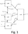
- Fig. 1 shows a block diagram of a power combiner circuit according to an embodiment, which serves to output power to a load 11 based on an input signal in.
- the power combiner circuit of Fig. 1 comprises n cells 10, where n is an integer number greater than 1 (i.e. at least 2).
- the individual cells are denoted with numerals 10_1, 10_2...10_N in Fig. 1 and will be collectively referred to as cells 10.
- each cell comprises one or more transistors.
- cells number 2 (cell 10_2) to the penultimate cell (cell 10_N-1) are implemented in the same manner.
- Cell 10 1 receives input signal in, for example at a control input (gate or base) of a transistor thereof.
- Each cell but the last cell i.e. cell 10_1 to cell 10_N-1) provides part of its output power to a load 11, as indicated by arrows 12_1, 12_2.
- Cell 10_N provides its complete output power to load 11, as indicated by an arrow 12_N. It should be noted that terms like "complete output power” or also a division of the output power as explained below is to be understood as comprising losses which always may happen in real implementations of systems.
- all cells but the last cell provide another part of their output power to the respective next cell (cell 1 to cell 2, cell 2 to cell 3, etc.), as indicated by arrows 13_1, 13_2...13_N-1.
- the partitioning of the output power between the load and the subsequent cell as will be explained later in some implementations, some problems which exist in conventional solutions may be overcome. For example, increasing source voltages at transistors in a conventional series connection may be avoided, and on the other hand, many transistors for power combination without the problems of stacked transistors experiencing a breakdown may be used.
- the number of cells is not particularly limited, and any number n of cells may be used. For example, up to 5 cells, up to 10 cells, up to 20 cells, up to 50 cells or even more cells may be used.
- the providing of partial power as indicated by arrows 12_1 to 12-N and 13_1 to 13_N-1 may be implemented using inductive couplings e.g. using transformers or inductively coupled lines between the cells and the load. Other couplings that provide DC decoupling and allow for a combining of power e.g. by a series connection on a side of load 11 may be used. For providing power to the respective next cell, any matching/splitting network may be used.
- the part of the power provided to the respective next cell may be smaller than the power provided to the load (for example the power provided according to arrow 13_1 may be smaller than the power provided according to arrow 12_1 for cell 10_1).
- the power provided to the respective next cell is at least 5%, at least 10% or at least 20% of the total output power of the respective cell.
- the power provided to the load is at least 30%, at least 40% or at least 50% of the total output power of the respective cell.
- the power provided to the respective next cell according to arrows 13 needs only be sufficient such that the respective next cell behave in accordance with the input signal in. In some other implementations an equal power split may be used in order to facilitate a simple implementation.
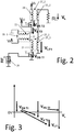
- Fig. 2 is a circuit diagram of a power combiner circuit according to an embodiment.
- the power combiner circuit comprises two cells, each cell comprising one transistor.
- a first cell in Fig. 2 comprises a transistor T 1 , a second primary side 22 and a first primary side 21.
- a second cell comprises a transistor T 2 , a second secondary side 23 and a first primary side 24.
- the power combiner circuit of Fig. 2 serves to provide power to a load RL coupled to a load output terminal of the power combiner circuit, which in Fig. 2 is symbolized by a resistor.
- a load may comprise resistive, inductive and/or capacitive components.
- the type of load is not particularly limited, and the depicted resistor serves only as a simple example. As shown in Fig.
- first secondary sides 25_1, 25_2 may be coupled in series with load RL and a load output terminal of the power combiner circuit may be a node between first secondary side 25_2 and load RL.
- a part of the power combiner circuit electrically coupled to the load, in this case first secondary sides 25_1, 25_2, may also be referred to as load output circuit herein.
- Second primary side 22 and second secondary side 23 form a transformer 26_1, first primary side 21 and first secondary side 25_1 form a transformer 27_1 and first primary side 24 and first secondary side 25_2 form a transformer 27_2.
- Each transformer 26_1, 27_1, 27_2 may comprise inductors on the respective primary and secondary side including series inductors, parallel inductors, parasitic inductors etc. and/or may comprise further components, for example for impedance matching, and/or components for transmitting signals like RF signals.
- the first cell receives a radio frequency input signal RF IN from a radio frequency source 20 at a gate terminal of transistor T 1 .
- Radio frequency source 20 may be any circuitry generating a radio frequency signal, for example circuitry in a mobile telecommunication application.
- Both cells are supplied by a supply voltage V D at drain terminals of transistors T 1 , T 2 , respectively, with respect to ground.
- Transistor T 1 acts as amplifier transistor of the first cell. Part of the power thus generated is transferred to the load by transformer 25_1. Another part of the power generated is transferred to the second cell through transformer 26_1.
- Transistor T 2 of the second cell is biased by a gate voltage V G2 to provide an adequate bias current similar to T 1 .
- the gate voltage V G2 may be variable.
- a DC part of the gate voltage V G2 may be fixed.
- a radio frequency (RF) network may be provided, for example implemented by a capacitive divider, which allows some voltage swing.
- the power generated by transistor T 2 is provided to load RL through transformer 27_2.
- the part of the output power of transistor T 1 transferred to the second cell via transformer 26_1 may be smaller than the part of the power provided directly to the load RL through transformer 27_1.
- the power provided to the second cell in some implementations need only be large enough to ensure a corresponding control of transistor T 2 by its gate source voltage.
- the ratio of the powers provided may be adjusted by designing the transformers 26_1, 27_1 accordingly.
- an appropriate source voltage for transistor T 2 may be adjusted by adjusting a turn ratio of transformer 26_1 accordingly.
- a drain source voltage of transistor T 1 , V DS T1 , a voltage across inductor 25_1, V LT1 , a voltage across a drain source voltage of transistor T 2 , V DS T2 , a source voltage of transistor T 2 , V S T2 , and a voltage across the load V L are denoted by arrows. Using these voltage, operation of the embodiment of Fig. 2 will be schematically explained with respect to Fig. 3 .
- the drain source voltage V DS T1 of transistor T 1 causes the voltage V LT1 (coupling of part of the power via transformer 27_1) and causes the source voltage V S T2 via transformer 26_1.
- a comparatively high load voltage V L is built up in this way by combining the voltage V LT1 at first secondary side 25_1 with the corresponding voltage at first secondary side 25_2 compared to the drain source voltages of the individual transistors, thus combining the power of the transistors and causing a level shifting.
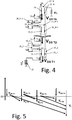
- Fig. 2 The approach shown for two cells in Fig. 2 may be extended to N cells, which is shown in Fig. 4 .
- N-2 intermediate cells are inserted in series.
- Each intermediate cell comprises a second secondary side 30, of which second secondary side 30_2 is shown for the second cell, a transistor, of which transistor T 2 is shown for the second cell, second primary side 32, of which a second primary side 32_N-1 is shown for the N-1-th cell and a first primary side 31, of which first primary side 31_N-1 is shown for the N-1-th cell.
- a respective first secondary side 25 25_1 to 25_n
- load RL for each cell, a respective first secondary side 25 (25_1 to 25_n) is provided coupled to load RL.
- the primary and secondary sides form transformers 26_1 to 26_N-1 and 27_1 to 27_N as defined in the general explanation of the terminology above.
- Each i-th intermediate cell receives power from the preceding cell via transformer 26_i-1.
- a part of the power generated by the transistor of the i-th intermediate cell is output to the load RL via the respective transformer 27_i.
- a part of the power generated in the i-th intermediate cell is provided to a respective next cell via transformer 26_i.
- the transistors of the second to N-th cells are biased by respective gate voltage V G2 ...V GN which may be equal to each other but which also may be unequal to each other and tailored to the respective source voltage received from the preceding cell.
- the explanations for gate voltage V G2 of Fig. 2 also apply to these gate voltages.
- drain source voltages of the transistors T 1 , T 2 ...T N are marked by arrows and labeled V DS T1 , V DS T2 ...V DS TN .
- part of the drain source voltage of each transistor contributes to the load voltage V L , and another, for example smaller, part generates the source voltage V S for the transistor of the respective next cells.
- the source voltages of transistors T 2 , T 3 , and T 4 thus generated may be approximately the same. This is unlike a conventional case, where in a series connections source voltages are built up.
- Fig. 14 illustrates a comparative example.
- Fig. 14 shows a comparative example of a series connections of cells without coupling of power from each cell to a load, which is done in the embodiment of Fig. 4 .
- Fig. 14 illustrates an example with four cells.
- Each cell comprises a transistor, labeled T 1 to T 4 .
- Transistor T 1 of the first cell receives a radio frequency input signal RF IN from a radio frequency source 130.
- Each of the first to fourth cell (comprising transistor T 1 to T 4 ) comprises a respective primary side 131 (labeled 131_1 to 131_4).
- Each of the second to fourth cell furthermore comprises a secondary side 132 (132_2 to 132_4) to form transistors 134_1 to 134_3 to receive power from the preceding cell.
- Primary sides 131 are coupled to the drain terminals of the transistors of the respective cell, and secondary sides 132 are coupled to the source terminals.
- Transistors T 2 to T 4 are biased by respective gate voltages V G2 to V G4 , which are adapted to the respective source voltages received to ensure a corresponding control of the transistors.
- the load receives power from the fourth cell through a transformer 134_4 including a secondary side 133 and a primary side 131_4.
- Fig. 14 furthermore, the drain source voltages of transistors T 1 to T 4 (V DS T1 to V DS T4 ) and the source voltages of transistors T 2 to T 4 (V S T2 to V S T4 ) are indicated.
- the complete power of a cell is provided to the respective next cell, by providing essentially a drain source voltage of a cell to the source of a transistor of a respective next cell. As further illustrated in Fig. 15 , this leads to an increase of the source voltage from stage to stage. Such high source voltages at some point may trigger parasitic source-bulk diodes or other parasitic elements, causing a malfunctioning of the power combiner and/or limiting the number of stages.
- the source voltages may be limited, and a breakdown involving such parasitics may be avoided in some implementations, as illustrated in Figs. 4 and 5 .
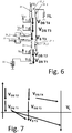
- Fig. 6 shows a circuit diagram of a power combiner circuit according to a further embodiment, which is based on the embodiment of Fig. 2 . Instead of providing one transistor in each cell, in Fig. 2 two stacked transistors are provided in each cell, T 1 and T 2 for the first cell and T 3 and T 4 for the second cell.
- stacking of transistors is a per se conventional technique for power combining, but the number of transistors that may be stacked in current transistor implementations is limited to two or three transistors due to breakdown considerations.
- this stacking of two transistors is combined with the techniques of Fig. 2 , and the power transfer between the cells and to the load correspond to the ones discussed with reference to Fig. 2 .
- each cell may be biased with twice the voltage V D of Fig. 2 , denoted with 2xV D in Fig. 6 .
- Transistor T 1 of the first cell is coupled to RF signal source 20, whereas the second transistor T 2 of the first cell and the transistors T 3 , T 4 of the second cell are biased by respective gate voltages V G2 , V G3 and V G4 , respectively.
- V G2 , V G3 and V G4 respectively.
- Fig. 6 the drain source voltages of transistors T 1 to T 4 (V DS T1 to V DS T4 ) are marked as well as the source voltage of transistor T 3 (V S T3 ), which receives its source voltage from the first cell.
- Fig. 7 shows the voltages in a diagram similar to the diagram of Fig. 3 . Also here, an increased load voltage V L may be obtained compared to the drain source voltages of the individual transistors.
- the limit for transistor stacking mentioned above may be circumvented, by providing only two or for example also three stacked transistors in each cell. Generally, the number of transistors in each cell are limited essentially by the breakdown voltage of the transistors, which depends on the implementation.
- Using stacked transistor in each cell may also be extended to more than two cells.
- a corresponding embodiment of a combiner circuit is illustrated in Fig. 8 .
- each cell has two stacked transistors (T 1 and T 2 for the first cell, T 3 and T 4 for the second cell... etc., up to T 2N-1 and T 2N for the N-th cell.
- Transistor T 1 receives the radio frequency input signal RF IN at a gate terminal thereof, whereas the other transistors are biased by respective gate voltages V G2 to V G2N .
- the individual cells are biased with a voltage 2xV D .
- the embodiment of Fig. 8 corresponds to the embodiment of Fig. 4 .
- transmission lines may be used to couple different parts of cells.
- Transmission lines are generally devices capable of transmitting radio frequency signals and may be implemented for example as so called microstrips or strip lines.
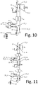
- Fig. 10 shows a combiner circuit according to an embodiment based on the embodiment of Fig. 2
- Fig. 11 shows a combiner circuit according to an embodiment based on the embodiment of Fig. 4 , where transmission lines are used to increase layout flexibility.
- Fig. 10 shows a combiner circuit according to an embodiment based on the embodiment of Fig. 2
- Fig. 11 shows a combiner circuit according to an embodiment based on the embodiment of Fig. 4 , where transmission lines are used to increase layout flexibility.
- Fig. 10 shows a combiner circuit according to an embodiment based on the embodiment of Fig. 2
- Fig. 11 shows a combiner circuit according to an embodiment based on the embodiment of Fig. 4 , where transmission lines are used to increase layout flexibility.
- Fig. 10 shows a combiner circuit according to an embodiment based on
- a transmission line TL 1 between first secondary sides 25_1 and 25_2 and a transmission line TL 2 between second secondary side 23 and transistor T 2 are used.
- other placements of transmission lines are possible, for example between transistor T 2 and inductor 24.
- Fig. 11 extends this concept to N cells, where corresponding transmission lines TL 1 , TL 2 ...TL 2N-1 , TL 2N-2 may be used. It should be noted that in yet other embodiments, transmission lines may be used only within some of the cells, whereas other cells may not have transmission lines.
- primary sides coupled in series are used to couple parts of a power of a cell directly to the load and another part to a next cell via the respective transformers including the primary sides.
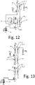
- Fig. 12 illustrates an embodiment based on the embodiment of Fig. 2 , where primary sides 21, 22 coupled in series are replaced by a second primary side 1122 and a first primary side 1121 coupled in parallel.
- a first primary side 1121 and a first secondary side 25_1 form transformer 27_1 to couple part of the power of the first cell to the load, and a second primary side 1122 and second secondary side 23 form transformer 26 1 to couple another part of the power to the second cell.
- This concept may be extended to more than one cell, for example also used in the embodiment of Fig. 4 . It should be noted that also mixed implementations are possible, where some cells use series coupling of primary sides and other cells use parallel couplings of primary sides.
- transformers 26_1 and 27_1 may be replaced by a trifilar transformer in other embodiments.
- the circuit of Fig. 12 may provide a lower load impedance which may help to increase output power.
- part of the power is provided from one cell to the next via a direct inductive coupling.
- an indirect coupling may be used.
- a power combiner circuit according to a corresponding embodiment is illustrated in Fig. 13 .
- Fig. 13 an example with two cells is shown, which again is a modification of the embodiment of Fig. 2 is.
- the variations illustrated with respect to Fig. 13 may also be applied to embodiments including more than two cells.
- the first cell including transistor T 1 includes only a single primary side 120, for coupling the power generated by T 1 to secondary side 25_1, which is coupled to load RL, via a transformer 122. Therefore, in this case, the complete output power is coupled to the load output circuit.
- a primary side 121 of the load output circuit is electrically coupled in series to inductor 25_1 and forms a transformer 123 with second secondary side 23 of the second cell, such that part of the power coupled from the first cell to the load output circuit is then provided from the load output circuit to the second cell.
- first secondary sides 25 and primary side 121 may be arranged in an alternating manner.
- Fig. 13 may help to decrease the complexity of the interconnects, as the cells do not have to be placed next to each other for a direct inductive coupling, but merely the electrical connection including first secondary sides 25_1, 25_2 and primary side 121 which is then coupled to the load RL is used to provide the connections and couplings.
- Fig. 16 is a flowchart illustrating a method according to an embodiment.
- the method of Fig. 16 may be implemented using any of the embodiments discussed above and, to avoid repetitions, will be described referring to these embodiments. However, it is to be understood that the method of Fig. 16 may also be implemented in other circuits.
- the method uses N cells, like cells 10 of Fig. 1 .
- the method comprises receiving an input signal, for example a radio frequency input signal like signal RF IN mentioned above, at a first cell of the N cells.
- the method comprises, at 1602, providing a first part of an output power of the i-th cell to a load (e.g. as represented by arrows 12_1, 12_2 in Fig. 1 ), and, at 1603, providing a second part of the output power to a respective next cell, i.e. i+1-th cell (e.g. as represented by arrows 13 in Fig. 1 ).
- the method comprises providing the output power of a last cell (i.e. N-th cell) to a load (e.g. as per arrow 12_N in Fig. 1 ).
Landscapes
- Engineering & Computer Science (AREA)
- Power Engineering (AREA)
- Microelectronics & Electronic Packaging (AREA)
- Amplifiers (AREA)
Priority Applications (1)
| Application Number | Priority Date | Filing Date | Title |
|---|---|---|---|
| EP19212569.8A EP3829059B1 (de) | 2019-11-29 | 2019-11-29 | Leistungskombinationsschaltung und verfahren |
Applications Claiming Priority (1)
| Application Number | Priority Date | Filing Date | Title |
|---|---|---|---|
| EP19212569.8A EP3829059B1 (de) | 2019-11-29 | 2019-11-29 | Leistungskombinationsschaltung und verfahren |
Publications (2)
| Publication Number | Publication Date |
|---|---|
| EP3829059A1 true EP3829059A1 (de) | 2021-06-02 |
| EP3829059B1 EP3829059B1 (de) | 2026-04-01 |
Family
ID=68732950
Family Applications (1)
| Application Number | Title | Priority Date | Filing Date |
|---|---|---|---|
| EP19212569.8A Active EP3829059B1 (de) | 2019-11-29 | 2019-11-29 | Leistungskombinationsschaltung und verfahren |
Country Status (1)
| Country | Link |
|---|---|
| EP (1) | EP3829059B1 (de) |
Citations (4)
| Publication number | Priority date | Publication date | Assignee | Title |
|---|---|---|---|---|
| US4743859A (en) * | 1986-05-16 | 1988-05-10 | The Marconi Company Limited | Amplifying circuit arrangement having means for distortion correction |
| US20070152751A1 (en) * | 2005-12-21 | 2007-07-05 | Trex Enterprises Corp. | Wide bandwidth, high power amplifier |
| US9369103B2 (en) * | 2014-03-03 | 2016-06-14 | Panasonic Corporation | Variable gain multistage amplifier and receiver |
| WO2017133776A1 (en) * | 2016-02-04 | 2017-08-10 | Fraunhofer-Gesellschaft zur Förderung der angewandten Forschung e.V. | Matrix power amplifier |
-
2019
- 2019-11-29 EP EP19212569.8A patent/EP3829059B1/de active Active
Patent Citations (4)
| Publication number | Priority date | Publication date | Assignee | Title |
|---|---|---|---|---|
| US4743859A (en) * | 1986-05-16 | 1988-05-10 | The Marconi Company Limited | Amplifying circuit arrangement having means for distortion correction |
| US20070152751A1 (en) * | 2005-12-21 | 2007-07-05 | Trex Enterprises Corp. | Wide bandwidth, high power amplifier |
| US9369103B2 (en) * | 2014-03-03 | 2016-06-14 | Panasonic Corporation | Variable gain multistage amplifier and receiver |
| WO2017133776A1 (en) * | 2016-02-04 | 2017-08-10 | Fraunhofer-Gesellschaft zur Förderung der angewandten Forschung e.V. | Matrix power amplifier |
Non-Patent Citations (1)
| Title |
|---|
| MING-FONG LEI ET AL: "Design and Analysis of Stacked Power Amplifier in Series-Input and Series-Output Configuration", IEEE TRANSACTIONS ON MICROWAVE THEORY AND TECHNIQUES, PLENUM, USA, vol. 55, no. 12, 1 December 2007 (2007-12-01), pages 2802 - 2812, XP011196326, ISSN: 0018-9480, DOI: 10.1109/TMTT.2007.909147 * |
Also Published As
| Publication number | Publication date |
|---|---|
| EP3829059B1 (de) | 2026-04-01 |
Similar Documents
| Publication | Publication Date | Title |
|---|---|---|
| CN108462477B (zh) | 功率放大电路 | |
| CN104660176B (zh) | 多赫蒂放大器 | |
| US11171616B2 (en) | Multi-branch outphasing system and method | |
| US12155352B2 (en) | Power amplifier arrangement | |
| US10432147B2 (en) | Inverted three-stage Doherty amplifier | |
| CN110690859B (zh) | 功率放大电路 | |
| US10530316B2 (en) | Matrix power amplifier | |
| US20050007194A1 (en) | Switched-mode power amplifier using lumped element impedance inverter for parallel combining | |
| US11309844B2 (en) | Power amplifier | |
| US12531525B2 (en) | Power amplifier circuit | |
| WO2023171364A1 (ja) | 高周波モジュールおよび通信装置 | |
| US10320335B1 (en) | Compact doherty power amplifier using non-uniform phase match devices | |
| US4733194A (en) | Apparatus and method for paralleling power field effect transistors in high frequency amplifiers | |
| EP3247041B1 (de) | Aktiver transformator, entsprechende vorrichtung und verfahren | |
| EP3829059B1 (de) | Leistungskombinationsschaltung und verfahren | |
| US20140333378A1 (en) | Circuit arrangement for generating a radio frequency signal | |
| CN113994592B (zh) | 具有大输出功率的功率放大器 | |
| KR101744005B1 (ko) | 병렬 보정 증폭기 | |
| CN118631191B (zh) | 用于w频段的多路功率放大器和射频模块 | |
| US20240364271A1 (en) | Inverted doherty-type amplifier device | |
| US20250202433A1 (en) | Combining network, and applications including doherty amplifiers | |
| EP4441890A1 (de) | Leistungskombinierer für leistungsverstärker |
Legal Events
| Date | Code | Title | Description |
|---|---|---|---|
| PUAI | Public reference made under article 153(3) epc to a published international application that has entered the european phase |
Free format text: ORIGINAL CODE: 0009012 |
|
| STAA | Information on the status of an ep patent application or granted ep patent |
Free format text: STATUS: THE APPLICATION HAS BEEN PUBLISHED |
|
| AK | Designated contracting states |
Kind code of ref document: A1 Designated state(s): AL AT BE BG CH CY CZ DE DK EE ES FI FR GB GR HR HU IE IS IT LI LT LU LV MC MK MT NL NO PL PT RO RS SE SI SK SM TR |
|
| STAA | Information on the status of an ep patent application or granted ep patent |
Free format text: STATUS: REQUEST FOR EXAMINATION WAS MADE |
|
| 17P | Request for examination filed |
Effective date: 20211201 |
|
| RBV | Designated contracting states (corrected) |
Designated state(s): AL AT BE BG CH CY CZ DE DK EE ES FI FR GB GR HR HU IE IS IT LI LT LU LV MC MK MT NL NO PL PT RO RS SE SI SK SM TR |
|
| STAA | Information on the status of an ep patent application or granted ep patent |
Free format text: STATUS: EXAMINATION IS IN PROGRESS |
|
| 17Q | First examination report despatched |
Effective date: 20230207 |
|
| GRAP | Despatch of communication of intention to grant a patent |
Free format text: ORIGINAL CODE: EPIDOSNIGR1 |
|
| STAA | Information on the status of an ep patent application or granted ep patent |
Free format text: STATUS: GRANT OF PATENT IS INTENDED |
|
| INTG | Intention to grant announced |
Effective date: 20251120 |
|
| GRAS | Grant fee paid |
Free format text: ORIGINAL CODE: EPIDOSNIGR3 |
|
| GRAA | (expected) grant |
Free format text: ORIGINAL CODE: 0009210 |
|
| STAA | Information on the status of an ep patent application or granted ep patent |
Free format text: STATUS: THE PATENT HAS BEEN GRANTED |
|
| P01 | Opt-out of the competence of the unified patent court (upc) registered |
Free format text: CASE NUMBER: UPC_APP_0002378_3829059/2026 Effective date: 20260122 |
|
| AK | Designated contracting states |
Kind code of ref document: B1 Designated state(s): AL AT BE BG CH CY CZ DE DK EE ES FI FR GB GR HR HU IE IS IT LI LT LU LV MC MK MT NL NO PL PT RO RS SE SI SK SM TR |
|
| REG | Reference to a national code |
Ref country code: CH Ref legal event code: F10 Free format text: ST27 STATUS EVENT CODE: U-0-0-F10-F00 (AS PROVIDED BY THE NATIONAL OFFICE) Effective date: 20260401 Ref country code: GB Ref legal event code: FG4D |
|
| REG | Reference to a national code |
Ref country code: DE Ref legal event code: R096 Ref document number: 602019083055 Country of ref document: DE |
|
| REG | Reference to a national code |
Ref country code: IE Ref legal event code: FG4D |