EP3830309B1 - Kupfer-silber-verbundstoff - Google Patents
Kupfer-silber-verbundstoff Download PDFInfo
- Publication number
- EP3830309B1 EP3830309B1 EP19749620.1A EP19749620A EP3830309B1 EP 3830309 B1 EP3830309 B1 EP 3830309B1 EP 19749620 A EP19749620 A EP 19749620A EP 3830309 B1 EP3830309 B1 EP 3830309B1
- Authority
- EP
- European Patent Office
- Prior art keywords
- silver
- copper
- approximately
- orthogonal
- dimensions
- Prior art date
- Legal status (The legal status is an assumption and is not a legal conclusion. Google has not performed a legal analysis and makes no representation as to the accuracy of the status listed.)
- Active
Links
Images

Classifications
-
- C—CHEMISTRY; METALLURGY
- C22—METALLURGY; FERROUS OR NON-FERROUS ALLOYS; TREATMENT OF ALLOYS OR NON-FERROUS METALS
- C22C—ALLOYS
- C22C9/00—Alloys based on copper
-
- B—PERFORMING OPERATIONS; TRANSPORTING
- B22—CASTING; POWDER METALLURGY
- B22F—WORKING METALLIC POWDER; MANUFACTURE OF ARTICLES FROM METALLIC POWDER; MAKING METALLIC POWDER; APPARATUS OR DEVICES SPECIALLY ADAPTED FOR METALLIC POWDER
- B22F1/00—Metallic powder; Treatment of metallic powder, e.g. to facilitate working or to improve properties
- B22F1/05—Metallic powder characterised by the size or surface area of the particles
- B22F1/054—Nanosized particles
- B22F1/0547—Nanofibres or nanotubes
-
- B—PERFORMING OPERATIONS; TRANSPORTING
- B22—CASTING; POWDER METALLURGY
- B22F—WORKING METALLIC POWDER; MANUFACTURE OF ARTICLES FROM METALLIC POWDER; MAKING METALLIC POWDER; APPARATUS OR DEVICES SPECIALLY ADAPTED FOR METALLIC POWDER
- B22F3/00—Manufacture of workpieces or articles from metallic powder characterised by the manner of compacting or sintering; Apparatus specially adapted therefor ; Presses and furnaces
- B22F3/10—Sintering only
- B22F3/105—Sintering only by using electric current other than for infrared radiant energy, laser radiation or plasma ; by ultrasonic bonding
-
- B—PERFORMING OPERATIONS; TRANSPORTING
- B22—CASTING; POWDER METALLURGY
- B22F—WORKING METALLIC POWDER; MANUFACTURE OF ARTICLES FROM METALLIC POWDER; MAKING METALLIC POWDER; APPARATUS OR DEVICES SPECIALLY ADAPTED FOR METALLIC POWDER
- B22F3/00—Manufacture of workpieces or articles from metallic powder characterised by the manner of compacting or sintering; Apparatus specially adapted therefor ; Presses and furnaces
- B22F3/12—Both compacting and sintering
- B22F3/16—Both compacting and sintering in successive or repeated steps
- B22F3/162—Machining, working after consolidation
-
- B—PERFORMING OPERATIONS; TRANSPORTING
- B22—CASTING; POWDER METALLURGY
- B22F—WORKING METALLIC POWDER; MANUFACTURE OF ARTICLES FROM METALLIC POWDER; MAKING METALLIC POWDER; APPARATUS OR DEVICES SPECIALLY ADAPTED FOR METALLIC POWDER
- B22F5/00—Manufacture of workpieces or articles from metallic powder characterised by the special shape of the product
- B22F5/12—Manufacture of workpieces or articles from metallic powder characterised by the special shape of the product of wires
-
- B—PERFORMING OPERATIONS; TRANSPORTING
- B22—CASTING; POWDER METALLURGY
- B22F—WORKING METALLIC POWDER; MANUFACTURE OF ARTICLES FROM METALLIC POWDER; MAKING METALLIC POWDER; APPARATUS OR DEVICES SPECIALLY ADAPTED FOR METALLIC POWDER
- B22F9/00—Making metallic powder or suspensions thereof
- B22F9/16—Making metallic powder or suspensions thereof using chemical processes
- B22F9/18—Making metallic powder or suspensions thereof using chemical processes with reduction of metal compounds
- B22F9/24—Making metallic powder or suspensions thereof using chemical processes with reduction of metal compounds starting from liquid metal compounds, e.g. solutions
-
- C—CHEMISTRY; METALLURGY
- C22—METALLURGY; FERROUS OR NON-FERROUS ALLOYS; TREATMENT OF ALLOYS OR NON-FERROUS METALS
- C22C—ALLOYS
- C22C1/00—Making non-ferrous alloys
- C22C1/04—Making non-ferrous alloys by powder metallurgy
- C22C1/0425—Copper-based alloys
-
- C—CHEMISTRY; METALLURGY
- C22—METALLURGY; FERROUS OR NON-FERROUS ALLOYS; TREATMENT OF ALLOYS OR NON-FERROUS METALS
- C22C—ALLOYS
- C22C47/00—Making alloys containing metallic or non-metallic fibres or filaments
- C22C47/14—Making alloys containing metallic or non-metallic fibres or filaments by powder metallurgy, i.e. by processing mixtures of metal powder and fibres or filaments
-
- C—CHEMISTRY; METALLURGY
- C22—METALLURGY; FERROUS OR NON-FERROUS ALLOYS; TREATMENT OF ALLOYS OR NON-FERROUS METALS
- C22C—ALLOYS
- C22C49/00—Alloys containing metallic or non-metallic fibres or filaments
- C22C49/14—Alloys containing metallic or non-metallic fibres or filaments characterised by the fibres or filaments
-
- B—PERFORMING OPERATIONS; TRANSPORTING
- B22—CASTING; POWDER METALLURGY
- B22F—WORKING METALLIC POWDER; MANUFACTURE OF ARTICLES FROM METALLIC POWDER; MAKING METALLIC POWDER; APPARATUS OR DEVICES SPECIALLY ADAPTED FOR METALLIC POWDER
- B22F2301/00—Metallic composition of the powder or its coating
- B22F2301/10—Copper
-
- B—PERFORMING OPERATIONS; TRANSPORTING
- B22—CASTING; POWDER METALLURGY
- B22F—WORKING METALLIC POWDER; MANUFACTURE OF ARTICLES FROM METALLIC POWDER; MAKING METALLIC POWDER; APPARATUS OR DEVICES SPECIALLY ADAPTED FOR METALLIC POWDER
- B22F2301/00—Metallic composition of the powder or its coating
- B22F2301/25—Noble metals, i.e. Ag Au, Ir, Os, Pd, Pt, Rh, Ru
- B22F2301/255—Silver or gold
-
- B—PERFORMING OPERATIONS; TRANSPORTING
- B22—CASTING; POWDER METALLURGY
- B22F—WORKING METALLIC POWDER; MANUFACTURE OF ARTICLES FROM METALLIC POWDER; MAKING METALLIC POWDER; APPARATUS OR DEVICES SPECIALLY ADAPTED FOR METALLIC POWDER
- B22F2304/00—Physical aspects of the powder
- B22F2304/10—Micron size particles, i.e. above 1 micrometer up to 500 micrometer
-
- B—PERFORMING OPERATIONS; TRANSPORTING
- B22—CASTING; POWDER METALLURGY
- B22F—WORKING METALLIC POWDER; MANUFACTURE OF ARTICLES FROM METALLIC POWDER; MAKING METALLIC POWDER; APPARATUS OR DEVICES SPECIALLY ADAPTED FOR METALLIC POWDER
- B22F2998/00—Supplementary information concerning processes or compositions relating to powder metallurgy
- B22F2998/10—Processes characterised by the sequence of their steps
-
- B—PERFORMING OPERATIONS; TRANSPORTING
- B22—CASTING; POWDER METALLURGY
- B22F—WORKING METALLIC POWDER; MANUFACTURE OF ARTICLES FROM METALLIC POWDER; MAKING METALLIC POWDER; APPARATUS OR DEVICES SPECIALLY ADAPTED FOR METALLIC POWDER
- B22F2999/00—Aspects linked to processes or compositions used in powder metallurgy
-
- C—CHEMISTRY; METALLURGY
- C22—METALLURGY; FERROUS OR NON-FERROUS ALLOYS; TREATMENT OF ALLOYS OR NON-FERROUS METALS
- C22C—ALLOYS
- C22C49/00—Alloys containing metallic or non-metallic fibres or filaments
- C22C49/02—Alloys containing metallic or non-metallic fibres or filaments characterised by the matrix material
-
- H—ELECTRICITY
- H01—ELECTRIC ELEMENTS
- H01B—CABLES; CONDUCTORS; INSULATORS; SELECTION OF MATERIALS FOR THEIR CONDUCTIVE, INSULATING OR DIELECTRIC PROPERTIES
- H01B1/00—Conductors or conductive bodies characterised by the conductive materials; Selection of materials as conductors
- H01B1/02—Conductors or conductive bodies characterised by the conductive materials; Selection of materials as conductors mainly consisting of metals or alloys
- H01B1/026—Alloys based on copper
-
- Y—GENERAL TAGGING OF NEW TECHNOLOGICAL DEVELOPMENTS; GENERAL TAGGING OF CROSS-SECTIONAL TECHNOLOGIES SPANNING OVER SEVERAL SECTIONS OF THE IPC; TECHNICAL SUBJECTS COVERED BY FORMER USPC CROSS-REFERENCE ART COLLECTIONS [XRACs] AND DIGESTS
- Y10—TECHNICAL SUBJECTS COVERED BY FORMER USPC
- Y10T—TECHNICAL SUBJECTS COVERED BY FORMER US CLASSIFICATION
- Y10T428/00—Stock material or miscellaneous articles
- Y10T428/12—All metal or with adjacent metals
- Y10T428/12014—All metal or with adjacent metals having metal particles
- Y10T428/12028—Composite; i.e., plural, adjacent, spatially distinct metal components [e.g., layers, etc.]
Definitions
- the invention relates to a massive composite material comprising copper and a volume quantity of silver less than 5% by volume, relative to the total volume of said material, a method of manufacturing said material, and the uses of said material in various applications.
- the invention applies typically, but not exclusively, to the fields of microelectronics, industrial magnetoforming, conductors for electrical and/or telecommunications cables, and conductors for pulsed magnets. More particularly, the invention relates to a composite material having both good mechanical properties, in particular in terms of resistance to breaking, and good electrical properties, in particular electrical conductivity.
- Pure copper has excellent electrical conductivity (100% IACS or International Annealed Copper Standard ), but has a low breaking strength, notably around 200-400 MPa.
- mechanically reinforced copper conductors have been proposed comprising grains of pure copper in the form of nanocrystals or nanograins, or grains formed of a copper alloy.
- Sakai et al. described [Acta Materialia, 1997, 45, 3, 1017-1023 ] a copper-silver alloy comprising 24% by mass of silver, having an optimized breaking strength of approximately 1.5 GPa.
- its electrical conductivity is approximately 65% IACS. This conductivity does not allow the alloy to be used in pulsed magnets which would then undergo a drastic increase in temperature, and/or in high voltage electrical cables.
- CN 102723144 B describes a copper-silver composite material comprising 24% by mass of silver, and having an acceptable breaking strength of approximately 970 MPa.
- the composite material is obtained by a process comprising a step of inserting a silver bar into a copper tube, an electron beam welding step under vacuum, a heat treatment step at 500-700°C , an extrusion step, then several wire drawing, annealing, and shaping steps to form a composite single strand.
- composite single strands eg 630 single strands
- the process is very long, energy-intensive and/or expensive since it requires numerous heat treatment and shaping steps.
- the materials of the prior art have improved mechanical properties, to the detriment of electrical conductivity.
- the methods of the prior art introduce internal defects such as grain boundaries, or stacking faults, which induce a reduction in the electrical conductivity of the material obtained.
- the processes are often long and/or expensive.
- the aim of the present invention is to overcome all or part of the drawbacks of the prior art and in particular to provide a composite material based on copper and silver, having improved electrical properties, in particular in terms of electrical conductivity. , while guaranteeing good mechanical properties, in particular in terms of resistance to breaking, said material being able to present performances suitable for use in the field of cables, in particular as an electrically conductive element of an energy cable and/or telecommunications, in the field of pulsed magnets, in the field of intense magnetic field installations and/or in the field of industrial magnetoforming.
- Another aim of the invention is to provide a simple and economical process for preparing such a material.
- the material of the invention has improved electrical properties, in particular in terms of electrical conductivity, while guaranteeing good mechanical properties, in particular in terms of resistance to breakage.
- it can have a conductivity greater than or equal to approximately 75% lACS, while guaranteeing a breaking strength of at least approximately 900 MPa.
- the copper and silver are preferably in the form of grains having at least one of their dimensions of sub-micron size (i.e. less than 1 ⁇ m).
- the copper is in the form of grains having at least one of their dimensions less than or equal to approximately 700 nm, preferably less than or equal to approximately 500 nm, of more preferably ranging from approximately 50 to 400 nm, and more preferably ranging from approximately 100 to 300 nm.
- the term "dimension” means the average dimension in number of all the grains of a given population, this dimension being conventionally determined by well-known methods of a person skilled in the art.
- the size of the grain(s) according to the invention can for example be determined by microscopy, in particular by scanning electron microscope (SEM) or by transmission electron microscope (TEM).
- the material of the invention is a composite material.
- the expression “composite material” means a material comprising at least one pure copper phase and at least one pure silver phase.
- said material is an assembly of at least copper grains and grains of silver, the grains of copper and the grains of silver not being mutually soluble.
- a copper-silver composite material differs from a copper-silver alloy in which copper is combined with silver, for example by fusion or mechanofusion.
- copper-silver alloys consist of a two-phase eutectic structure in the form of copper-silver solid solutions, one rich in copper, and the other rich in silver.
- the composite material of the invention does not include a zone of mutual solubility of copper and silver. The absence of a zone of mutual solubility of copper and silver in the composite material of the invention can in particular be demonstrated by energy dispersive analysis (EDX).
- EDX energy dispersive analysis
- the material of the invention is massive. In other words, it is in the form of a solid mass, or it is different from a material in the form of a powder or powdery material.
- the material of the invention preferably has a conductivity of at least approximately 80% IACS, more preferably at least approximately 85% IACS, and more preferably at least approximately 90% IACS, in particular at 20°C. .
- the material of the invention preferably has an electrical resistivity of at most approximately 2.15 ⁇ .cm, more preferably at most approximately 2.03 ⁇ .cm, and more preferably at most 1.91 approximately ⁇ .cm, particularly at 20°C.
- the material of the invention preferably has an electrical resistivity of at most approximately 0.70 ⁇ .cm, more preferably at most approximately 0.60 ⁇ .cm, and more preferably at most 0.50 approximately ⁇ .cm, particularly at -196°C.
- the electrical resistivity is preferably determined using a device sold under the trade name Sourcemeter KEITHLEY2450, by the company TEKTRONIX.
- the material of the invention preferably has a breaking strength of at least 900 MPa, preferably at least 1 GPa, preferably at least approximately 1.05 GPa, more preferably at least 1 .1 GPa approximately, and more preferably at least 1.2 GPa approximately, in particular at -196°C.
- the breaking strength is preferably determined using a device sold under the trade name INSTRON 1195, by the company INSTRON.
- the material of the invention preferably has an elongation at break of at least approximately 0.5%, particularly at room temperature (i.e. 18-25°C).
- the elongation at break is preferably determined using a device sold under the trade name Epsilon 3442 extensometer, by the company DOERLER Mesures.
- the material comprises silver in a volume proportion of less than 5%, relative to the total volume of said material.
- the low proportion of silver in said material makes it possible to guarantee a homogeneous material, in which the silver grains are uniformly dispersed within the copper grains. Indeed, at 5% by volume or beyond, the dispersion of silver in the material is heterogeneous (e.g. presence of aggregates), leading to a weakening of its mechanical properties.
- the material comprises at most approximately 2% by volume of silver, preferably at most approximately 1.5% by volume of silver, and even more preferably at most 1% by volume. Approximately % by volume of silver, relative to the total volume of said material.
- the material of the invention comprises at least 0.1% by volume of silver, and preferably at least 0.5% by volume of silver, relative to the total volume of said material.
- the material of the invention may comprise at least approximately 98% by volume of copper, and preferably at least 99% by volume of copper, relative to the total volume of said material.
- the material of the invention may comprise at most approximately 99.9% by volume of copper, and preferably at most 99.5% by volume of copper, relative to the total volume of said material.
- the material comprises at most approximately 0.1% by volume of unavoidable impurities, relative to the total volume of said material.
- the unavoidable impurities can be chosen from the elements Al, C, Fe, Ni, Pb, Si, Sn, Zn, Se, and one of their mixtures.
- the material comprises at most approximately 0.5% by volume, and preferably at most approximately 0.1% by volume, of other impurities chosen from O, S, P, Se, and one of their mixtures.
- the material essentially comprises copper and silver.
- copper and silver represent at least 99.9% by volume, and more preferably approximately 100% by volume, relative to the total volume of said material.
- the copper and/or silver are in the form of grains having a filamentary shape.
- the material of the invention is preferably anisotropic. In other words, it is composed of copper grains (respectively silver) elongated in a preferred direction, also called filamentary grains.
- a grain having a filamentary shape can be a “ribbon” in which the two orthogonal dimensions (D Cu1 , D Cu2 ) of the grain according to the invention are its width (I cu ) (first orthogonal dimension ) and its thickness (E Cu ) (second orthogonal dimension), the width (I cu ) being notably much greater than the thickness (E Cu ).
- the two orthogonal dimensions (D Ag1 , D Ag2 ) of a grain having a filamentary shape are equivalent or close. We then speak of a “stick” or “thread”.
- the length (L Ag ) of the silver grains can be of micrometric size (ie less than 1 mm), preferably less than or equal to approximately 500 ⁇ m, preferably less than or equal to approximately 200 ⁇ m, more preferably ranging from 1 at approximately 150 ⁇ m, and more preferably ranging from approximately 10 to 70 ⁇ m.
- the process of the invention is simple and it allows in a few steps to obtain a composite material conforming to the first object of the invention, having improved electrical properties, in particular in terms of electrical conductivity, while guaranteeing good mechanical properties, particularly in terms of breaking strength. Furthermore, it avoids repeated annealing and/or heat treatment steps such as those carried out in the processes of the prior art, while avoiding the phenomena of diffusion and/or melting of copper and silver. Finally, such a process can easily be transposed to an industrial scale.
- Step i) makes it possible to form a homogeneous mixture of copper and silver, while avoiding metal diffusion phenomena.
- the non-solvent medium can be chosen from alcohols, water, ketones such as acetone, and one of their mixtures.
- the non-solvent media S 1 and S 2 can have the same definition as that given above for the non-solvent medium S.
- the non-solvent media S 1 and S 2 are identical.
- the non-solvent media S 1 and S 2 are preferably mutually soluble.
- Substep i-a) can be carried out with mechanical or magnetic stirring or in the presence of ultrasound.
- Substep i-b) can be carried out with mechanical or magnetic stirring, in particular in order to avoid the degradation of the micrometric or sub-micrometric silver particles.
- Substep i-c) can be carried out with mechanical or magnetic stirring or in the presence of ultrasound.
- the micrometric copper particles can have at least one of their dimensions ranging from approximately 0.5 to 20 ⁇ m, preferably from 0.5 to 10 ⁇ m approximately, preferably from approximately 0.5 to 4 ⁇ m, and more preferably from approximately 0.5 to 1.5 ⁇ m.
- micrometric copper particles are preferably spherical micrometric particles.
- the silver particles can have at least one of their dimensions ranging from approximately 0.1 to 150 ⁇ m, and preferably from approximately 0.5 to 70 ⁇ m.
- micrometric or sub-micrometric particles of silver can be spherical or filiform.
- the micrometric or sub-micrometric spherical silver particles may have a diameter ranging from approximately 0.5 to 20 ⁇ m, preferably from approximately 0.5 to 10 ⁇ m, preferably from approximately 0.5 to 4 ⁇ m, and preferably another approximately 0.5 to 1.5 ⁇ m.
- the micrometric or sub-micrometric silver particles are filiform.
- the two orthogonal dimensions (D' Ag1 , D' Ag2 ) of a filiform particle are equivalent or close and represent the diameter (D' Ag ) of its cross section. We then speak of a “stick” or “thread”.
- a filiform particle is a “ribbon” in which the two orthogonal dimensions of the particle according to the invention are its width (I' Ag ) (first orthogonal dimension) and its thickness (E' Ag ) (second orthogonal dimension), the width (I' Ag ) being notably much greater than the thickness (E' Ag ).
- Step ii) allows the non-solvent media to evaporate.
- the drying temperature preferably ranges from approximately 70 to 100°C, and is more preferably of the order of 80°C.
- the composite powder comprises at most approximately 2% by volume of silver particles, preferably at most approximately 1.5% by volume of silver particles, and even more more preferentially at most approximately 1% by volume of silver particles, relative to the total volume of said powder.
- the process may further comprise a step ii') of reduction of the dried composite powder from step ii), in the presence of dihydrogen.
- This step ii') can make it possible to eliminate the layer of copper oxide which can form on the surface of the copper particles.
- Step ii') can be carried out at a temperature T 1 of approximately 100 to 300°C, preferably of approximately 110 to 240°C, and more preferably of approximately 120 to 160°C.
- Step ii') can be carried out by heating the powder from room temperature to temperature T 1 as defined in the invention, at a speed ranging from 1°C/min to approximately 5°C/min, and preferably still ranging from approximately 2°C/min to 3°C/min.
- Flash sintering means uniaxial pressure sintering based on the use of an electric current. Flash sintering is also well known as “ Spark Plasma Sintering” or SPS.
- Step iii) makes it possible to consolidate the powder obtained in the previous step ii) or ii'), while avoiding the phenomena of diffusion and/or melting of the copper and/or silver.
- This step iii) is preferably carried out at a temperature T 2 of at most approximately 550°C, preferably ranging from approximately 375 to 525°C, and even more preferably ranging from approximately 390 to 450°C. These temperatures make it possible to obtain a solid composite mass having sufficient residual porosity to be able to be cold drawn in the subsequent stages (eg without breaks and/or cracks and/or ruptures).
- Sintering is preferably carried out under primary or secondary vacuum, or under an argon or nitrogen atmosphere.
- the pressure exerted on the composite powder resulting from step ii) or ii') preferably ranges from 20 to 100 MPa, and even more preferably from 25 to 35 MPa.
- the duration of sintering varies depending on the temperature. This duration generally ranges from approximately 20 to 30 minutes.
- the sintering is carried out under secondary vacuum, at a pressure of approximately 25 to 50 MPa, at a maximum temperature of 400 to 500°C, maintained for a period of 3 to 10 minutes .
- the total duration of the heat treatment is, in this case, less than 1 hour 30 minutes.
- the intensity of the pulsed current can range from approximately 10 to 250 A.
- the duration of each current pulse is of the order of a few milliseconds. This duration preferably ranges from approximately 2 to 4 ms.
- the composite solid mass obtained at the end of step iii) has a relative density ranging from approximately 85 to 97%, preferably from approximately 90 to 95%, and more preferably from approximately 92 to 96%.
- these density ranges are adapted to be able to implement the following wire drawing step, avoiding the formation of cracks and/or fractures.
- the composite material can be in the form of a cylinder or a bar, in particular having a height or length greater than its diameter. This can thus make it possible to promote the implementation of step iv).
- the cylinder or bar has a diameter ranging from approximately 5 to 80 mm, and preferably from approximately 5 to 40 mm.
- Step iii) makes it possible to preserve the micrometric size of the copper particles and the micrometric or sub-micrometric size of the silver particles, and thus to avoid the growth of metallic grains.
- the solid composite mass obtained in step iii) is preferably isotropic. In other words, it does not present a preferential orientation of the copper grains (respectively silver), compared to its own macroscopic geometric shape.
- the cold drawing step(s) iv) are preferably carried out at a temperature of at most approximately 40°C, preferably at most approximately 35°C, particularly preferably ranging from -196°C to 30°C. C approximately, and more particularly preferably at room temperature.
- the ambient temperature corresponds to a temperature ranging from approximately 18 to 25°C.
- the process can comprise several steps iv), in particular from approximately 20 to 80 steps iv), and in particular around forty steps iv).
- the drawing step(s) iv) make it possible to obtain a composite material in the form of a wire, in particular with a diameter ranging from approximately 0.1 to 4 mm, preferably from 0.2 to 4 mm. approximately 1 mm, and more preferably approximately 0.25 to 0.8 mm.
- the drawing step(s) iv) make it possible to obtain a composite material in the form of a wire of length ranging from approximately 0.1 to 1000 m, and preferably from 0.2 to 50 m approximately.
- step iv the phenomena of rupture and/or cracks and/or breaks are greatly reduced, or even avoided.
- the method may further comprise between steps iii) and iv) a step of cooling the solid composite mass, in particular at a cooling rate ranging from approximately 4°C/min to 7°C/min.
- the process conforming to the second object leads to a material conforming to the first object.
- the invention also relates to a massive composite material as defined in the first subject of the invention, capable of being obtained according to a process as defined in the second subject of the invention.
- the third object of the invention is the use of a massive composite material conforming to the first object of the invention or obtained according to a process conforming to the second object of the invention, as an electrical conductor, in particular for electrical cables and/or telecommunications, as a conductor for continuous or pulsed field magnets, in the field of intense field installations, or in the field of industrial magnetoforming.
- Such a massive composite material presents a good compromise between electrical conduction and breaking strength to be able to be used in high voltage cables or overhead electricity transmission lines, in particular as an electrical conductor, or in motors, alternators, transformers, or connectors.
- the massive composite material conforming to the first object of the invention can also be used in installations with intense magnetic fields, in particular non-destructive pulsed magnetic fields greater than 100 Tesla.
- the low electrical resistivity of this material can induce, at constant power, an increase in the duration of the pulse of the pulsed magnetic field and a reduction in the electrical power necessary to power the continuous magnets.
- wires made of solid composite material conforming to the first object of the invention can be integrated into prototypes of magnetoforming magnets.
- Wires made of solid composite material conforming to the first object of the invention can enable the winding of industrial magnets for magnetoforming.
- Silver nanowires were prepared using a solution growth method from silver nitrate (AgNO 3 ), PVP, and ethylene glycol, as described by Sun YG et al., “Crystalline silver nanowires by soft solution processing,”. Nano Letters, 2002. 2(2): p. 165-168 , with a PVP/AgNO 3 ratio of 1.53.
- the silver nanowires obtained have a length ranging from approximately 30 to 60 ⁇ m, and a diameter ranging from approximately 200 to 300 nm.
- a suspension comprising 0.178 g of silver nanowires and 9 ml of ethanol was prepared.
- the suspension of silver nanowires was mixed with 15 g of copper powder, then the resulting mixture was homogenized under ultrasound, then evaporated using a rotary evaporator at 80°C.
- a PC 1 composite powder comprising 1% by volume of silver, relative to the total volume of the powder, was thus obtained.
- the composite powder was reduced in the presence of dihydrogen for 1 h at 160°C in order to reduce the copper oxide formed on the surface of the copper particles.
- the resulting powder was then sintered by SPS using a device sold under the trade name Dr Sinter 2080® , by the company Syntex Inc.
- the composite powder was placed in a die/matrix made of tungsten carbide and cobalt alloy (WC/Co) with an internal diameter of 8 mm, the interior of which was protected by a graphite film.
- the die was then closed by symmetrical pistons and then introduced into the chamber of the SPS machine.
- Sintering was carried out under vacuum (chamber residual pressure ⁇ 10 Pa) using pulsed direct currents defined over 14 periods of 3.2 ms, including 12 pulse periods and 2 non-pulse periods.
- the temperature was controlled using a thermocouple inserted into a hole (5 mm deep) drilled on the external surface of the die.
- a temperature of 500°C was reached in 2 stages: a ramp of 25°C.min -1 for 13 minutes to go from ambient temperature to 350°C, then a ramp of 50°C.min -1 for 3 minutes to go from 350°C to 500°C. This temperature was then maintained for 5 minutes. These temperature ramps were obtained by applying pulsed direct currents defined over 14 periods of 3.2 ms, including 12 pulse periods and 2 non-pulse periods. A pressure of 25 MPa was reached within 1 minute and maintained for the remainder of the sintering. The die was then cooled within the SPS chamber.
- the MSC 1 composite solid mass obtained is in the form of a cylinder of 8 mm in diameter and 33 mm in length.
- the composite solid mass obtained was then drawn at room temperature using a tungsten carbide die. After 40 passes, a composite material in the form of an FC 1 wire of 0.29 mm in diameter and 25 m in length was obtained. No breakage of the wires was observed.
- the composite powders and composite wires were analyzed by scanning electron microscopy (SEM) using a field effect gun, sold under the trade name JEOL JSM 6700F by the company JEOL, and operating at 200 kV.
- SEM scanning electron microscopy
- the density of the composite solid masses and the composite wires was determined by the Archimedes method.
- the electrical resistivity of the composite wires was determined to be 77K (liquid nitrogen) using the four-point method, with a maximum current of 100 mA to avoid heating of the wires.
- the breaking strength was measured using a device sold under the trade name INSTRON 1195 by the company INSTRON, at 77K (liquid nitrogen) and at 293K on composite wires 170 mm long.
- the specific tensions encountered were measured with a force sensor (1000 N or 250 N; 1.6 X 10 -5 ms -1 ).
- the density of the composite solid masses MSC 1 and MSC A is approximately 94% ( ⁇ 2%).
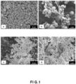
- FIG 1 is a SEM image of the PC 1 composite powder according to the invention (cf. figure 1a : scale 10 ⁇ m, and figure 1b : scale 2 ⁇ m), and the PC A composite not in accordance with the invention (cf. figure 1c : scale 10 ⁇ m, and figure 1d : scale 2 ⁇ m).
- figure 1 shows the uniform dispersion of the silver nanowires within the copper powder, inducing a homogeneous powder.
- the use of a volume quantity of silver of approximately 10% by volume does not make it possible to obtain a homogeneous powder.
- FIG. 2 shows the resistivity (in pQ.cm) at 77K of a composite material in the form of an FC 1 wire in accordance with the invention (curve with solid triangles) and of a composite material in the form of a wire FC A not in accordance with the invention (curve with solid circles), depending on their respective diameter (in mm).
- FIG. 3 shows the breaking strength (in MPa) at 77K of a composite material in the form of an FC 1 wire in accordance with the invention (curve with solid triangles) and of a composite material in the form of a FC A wire not in accordance with the invention (curve with solid circles), depending on their respective diameter (in mm).
- the breaking strength at 77K of a composite wire according to the invention is twice that of a pure copper wire with equivalent diameters, while guaranteeing low electrical resistivity (0.38-0.50 pQ .cm). These electrical resistivity values are in particular lower than those obtained for alloys or composites of the prior art having a similar breaking strength, but comprising 20 times more silver.
Landscapes
- Chemical & Material Sciences (AREA)
- Engineering & Computer Science (AREA)
- Mechanical Engineering (AREA)
- Manufacturing & Machinery (AREA)
- Materials Engineering (AREA)
- Metallurgy (AREA)
- Organic Chemistry (AREA)
- Nanotechnology (AREA)
- Physics & Mathematics (AREA)
- Optics & Photonics (AREA)
- Chemical Kinetics & Catalysis (AREA)
- General Chemical & Material Sciences (AREA)
- Inorganic Chemistry (AREA)
- Conductive Materials (AREA)
- Powder Metallurgy (AREA)
- Manufacture Of Metal Powder And Suspensions Thereof (AREA)
Claims (14)
- Material, umfassend Kupfer und Silber, dadurch gekennzeichnet, dass es ein massiver Verbundstoff ist, enthaltend Kupferkörner und Silberkörner, die nicht gegenseitig löslich sind, und dadurch, dass es eine Volumenmenge Silber von mindestens 0,1 Volumenprozent und weniger als 5 Volumenprozent mit Bezug auf das Gesamtvolumen des Materials umfasst, wobei das Kupfer und das Silber mindestens 99,9 Volumenprozent mit Bezug auf das Gesamtvolumen des Materials darstellen, und wobei das Silber und das Kupfer die Form von Körnern mit einer Fadenform aufweisen.
- Material nach Anspruch 1, dadurch gekennzeichnet, dass das Kupfer und das Silber die Form von Körnern aufweisen, wobei mindestens eine ihrer Abmessungen kleiner als oder gleich wie 500 nm ist.
- Material nach Anspruch 1 oder 2, dadurch gekennzeichnet, dass es eine Leitfähigkeit von mindestens 80 % IACS aufweist.
- Material nach einem der vorhergehenden Ansprüche, dadurch gekennzeichnet, dass es eine Bruchfestigkeit von mindestens 1 GPa aufweist.
- Material nach einem der vorhergehenden Ansprüche, dadurch gekennzeichnet, dass es höchstens 1,5 Volumenprozent Silber mit Bezug auf das Gesamtvolumen des Materials umfasst.
- Material nach einem der vorhergehenden Ansprüche, dadurch gekennzeichnet, dass die Kupferkerne Folgendes aufweisen:- eine Länge (LCu), die sich gemäß einer Hauptdehnungsrichtung erstreckt,- zwei Abmessungen (DCu1) und (DCu2),bezeichnet als orthogonale Abmessungen, die sich gemäß zwei Querrichtungen orthogonal zueinander und orthogonal zu der Hauptdehnungsrichtung erstrecken, wobei die orthogonalen Richtungen (DCu1) und (DCu2) kleiner als die Länge (LCu) sind und von 50 bis 400 nm reichen, und- zwei Beziehungen (FCu1) und (FCu2), bezeichnet als Formfaktoren, zwischen der Länge (LCu), und jeder der zwei orthogonalen Abmessungen (DCu1) und (DCu2),wobei die Formfaktoren (FCu1) und (FCu2) grösser als oder gleich wie 75 sind, und die Silberkörner Folgendes aufweisen:- eine Länge , die sich gemäß einer Hauptdehnungsrichtung erstreckt,- zwei Abmessungen (DAg1) und (DAg2), bezeichnet als orthogonale Abmessungen, die sich gemäß zwei Querrichtungen orthogonal zueinander und orthogonal zu der Hauptdehnungsrichtung erstrecken, wobei die orthogonalen Abmessungen (DAg1) und (DAg2) kleiner als die Länge (LAg) sind und von 50 bis 400 nm reichen, und- zwei Beziehungen (FAg1) und (FAg2), bezeichnet als Formfaktoren, zwischen der Länge (LAg) und jeder der zwei orthogonalen Abmessungen (DAg1) und (DAg2), wobei die Formfaktoren (FA91, FAg2) grösser als oder gleich wie 75 sind.
- Verfahren zur Herstellung eines massiven Verbundstoffs wie in einem der Ansprüche 1 bis 6 definiert, dadurch gekennzeichnet, dass es mindestens die folgenden Schritte umfasst:i) einen Schritt des Dispergierens von mikrometrischen Kupferpartikeln und mikrometrischen oder submikrometrischen Silberpartikeln in einem Nicht-Lösemittel-Medium,ii) einen Schritt des Trocknens, um ein Verbundpulver zu bilden, das die Kupfer- und Silberpartikel umfasst, wobei das Pulver eine Menge von weniger als 5 Volumenprozent Silberpartikel mit Bezug auf das Gesamtvolumen des Pulvers umfasst,iii) einen Schritt des Spark-Plasma-Sintering bei einer Temperatur von höchstens 600 °C, um eine feste Verbundmasse zu erhalten, undiv) mindestens einen Schritt des Kaltziehens,um die feste Verbundmasse von Schritt iii) in Form zu bringen.
- Verfahren nach Anspruch 7, dadurch gekennzeichnet, dass das Nicht-Lösemittel-Medium von Schritt i) ausgewählt ist aus den Alkoholen, dem Wasser, den Ketonen und einer ihrer Mischungen.
- Verfahren nach Anspruch 7 oder 8, dadurch gekennzeichnet, dass die mikrometrischen Kupferpartikel mindestens eine Abmessung aufweisen, die von 0,5 bis 20 µm reicht.
- Verfahren nach einem der Ansprüche 7 bis 9, dadurch gekennzeichnet, dass die mikrometrischen oder submikrometrischen Silberpartikel fadenförmige Partikel sind, die Folgendes aufweisen:- eine Länge (L'Ag), die sich gemäß einer Hauptdehnungsrichtung erstreckt,- zwei Abmessungen (D'Ag1) und (D'Ag2), bezeichnet als orthogonale Abmessungen, die sich gemäß zwei Querrichtungen orthogonal zueinander und orthogonal zu der Hauptdehnungsrichtung erstrecken, wobei die orthogonalen Abmessungen (D'Ag1) und (D'Ag2) kleiner als die Länge (L'Ag) sind, und- zwei Beziehungen (F'Ag1) und (F'Ag2), bezeichnet als Formfaktoren, zwischen der Länge (LAg1) und jeder der zwei orthogonalen Abmessungen (D'Ag1) und (D'Ag2), und gekennzeichnet durch mindestens eine der folgenden Eigenschaften:- die zwei orthogonalen Abmessungen (D'Ag1, D'Ag2) der fadenförmigen Partikel reichen von 50 nm bis 400 nm;- die Länge (L'Ag) reicht von 1 µm bis 150 µm;- die Formfaktoren (F'Ag1, F'Ag2) sind grösser als oder gleich wie 75.
- Verfahren nach einem der Ansprüche 7 bis 10, dadurch gekennzeichnet, dass Schritt iii) bei einer Temperatur durchgeführt wird, die von 375 bis 525 °C reicht.
- Verfahren nach einem der Ansprüche 7 bis 10, dadurch gekennzeichnet, dass die feste Verbundmasse, erhalten am Ende von Schritt iii), eine relative Dichte aufweist, die von 85 bis 97 % reicht.
- Verfahren nach einem der Ansprüche 8 bis 13, dadurch gekennzeichnet, dass es außerdem einen Schritt ii') des Reduzierens des getrockneten Verbundpulvers von Schritt ii) in Anwesenheit von Dihydrogen umfasst.
- Verwendung eines massiven Verbundstoffs wie in einem der Ansprüche 1 bis 6 definiert, als elektrischen Leiter, als Leiter für Magnete mit kontinuierlichem oder gepulstem Feld auf dem Gebiet der Installationen mit starken Feldern oder auf dem Gebiet der industriellen Magnetumformung.
Applications Claiming Priority (2)
| Application Number | Priority Date | Filing Date | Title |
|---|---|---|---|
| FR1857040A FR3084376B1 (fr) | 2018-07-27 | 2018-07-27 | Materiau composite cuivre-argent |
| PCT/EP2019/069990 WO2020020986A1 (fr) | 2018-07-27 | 2019-07-25 | Matériau composite cuivre-argent |
Publications (3)
| Publication Number | Publication Date |
|---|---|
| EP3830309A1 EP3830309A1 (de) | 2021-06-09 |
| EP3830309B1 true EP3830309B1 (de) | 2024-05-22 |
| EP3830309C0 EP3830309C0 (de) | 2024-05-22 |
Family
ID=63963183
Family Applications (1)
| Application Number | Title | Priority Date | Filing Date |
|---|---|---|---|
| EP19749620.1A Active EP3830309B1 (de) | 2018-07-27 | 2019-07-25 | Kupfer-silber-verbundstoff |
Country Status (5)
| Country | Link |
|---|---|
| US (1) | US20210323060A1 (de) |
| EP (1) | EP3830309B1 (de) |
| JP (1) | JP7432577B2 (de) |
| FR (1) | FR3084376B1 (de) |
| WO (1) | WO2020020986A1 (de) |
Families Citing this family (3)
| Publication number | Priority date | Publication date | Assignee | Title |
|---|---|---|---|---|
| TWI768097B (zh) * | 2017-08-10 | 2022-06-21 | 日商田中貴金屬工業股份有限公司 | 高強度與高導電性的銅合金板材及其製造方法 |
| CN114669979A (zh) * | 2022-05-30 | 2022-06-28 | 昆明理工大学 | 一种表面带花纹的铜银合金的制备方法 |
| CN120715220A (zh) * | 2025-07-08 | 2025-09-30 | 西北有色金属宝鸡创新研究院 | 一种原位Ag NWs纤维增强的Cu-Ag合金线材制备方法 |
Family Cites Families (15)
| Publication number | Priority date | Publication date | Assignee | Title |
|---|---|---|---|---|
| US3401024A (en) * | 1965-10-04 | 1968-09-10 | Mallory & Co Inc P R | Electrical contact material |
| JP5162383B2 (ja) * | 2008-09-09 | 2013-03-13 | 国立大学法人東北大学 | 銀被覆銅微粉の製造方法 |
| JP2010065265A (ja) * | 2008-09-10 | 2010-03-25 | Hitachi Ltd | 金属ナノ粒子及びその複合粉末の作製方法 |
| US9017449B2 (en) * | 2010-12-09 | 2015-04-28 | Carestream Health, Inc. | Nanowire preparation methods, compositions, and articles |
| JP5202714B1 (ja) * | 2011-11-18 | 2013-06-05 | 田中貴金属工業株式会社 | 金属配線形成用の転写基板及び前記転写用基板による金属配線の形成方法 |
| CN102723144B (zh) | 2012-06-19 | 2013-12-18 | 西北有色金属研究院 | 一种Cu-Ag多芯复合线材的制备方法 |
| JP6281900B2 (ja) * | 2014-01-08 | 2018-02-21 | 国立大学法人東北大学 | 機能性焼結緻密膜の形成方法およびナノ粒子合成方法 |
| KR20150145892A (ko) * | 2014-06-19 | 2015-12-31 | (주)바이오니아 | 은 코팅 구리 나노 와이어 및 이의 제조 방법 |
| WO2017038465A1 (ja) * | 2015-08-31 | 2017-03-09 | 三井金属鉱業株式会社 | 銀被覆銅粉 |
| JP2017082263A (ja) * | 2015-10-26 | 2017-05-18 | Dowaエレクトロニクス株式会社 | 金属複合粉末およびその製造方法 |
| CN106493353A (zh) * | 2016-12-06 | 2017-03-15 | 江苏大学 | 一种铜银基自润滑复合材料及其制备方法 |
| CN106939381A (zh) * | 2017-03-30 | 2017-07-11 | 江苏大学 | 一种铜银基自润滑复合材料及其制备方法 |
| TWI768097B (zh) * | 2017-08-10 | 2022-06-21 | 日商田中貴金屬工業股份有限公司 | 高強度與高導電性的銅合金板材及其製造方法 |
| CN109590481A (zh) * | 2019-01-30 | 2019-04-09 | 北京科技大学 | 一种Cu2-xMxSe合金系列热电材料的高压制备方法 |
| KR102302548B1 (ko) * | 2020-06-29 | 2021-09-16 | 마이크로컴퍼지트 주식회사 | 표면 처리된 금속 나노와이어의 제조방법 |
-
2018
- 2018-07-27 FR FR1857040A patent/FR3084376B1/fr active Active
-
2019
- 2019-07-25 EP EP19749620.1A patent/EP3830309B1/de active Active
- 2019-07-25 WO PCT/EP2019/069990 patent/WO2020020986A1/fr not_active Ceased
- 2019-07-25 JP JP2021503852A patent/JP7432577B2/ja active Active
- 2019-07-25 US US17/263,199 patent/US20210323060A1/en not_active Abandoned
Also Published As
| Publication number | Publication date |
|---|---|
| JP2021531409A (ja) | 2021-11-18 |
| US20210323060A1 (en) | 2021-10-21 |
| EP3830309C0 (de) | 2024-05-22 |
| WO2020020986A1 (fr) | 2020-01-30 |
| JP7432577B2 (ja) | 2024-02-16 |
| FR3084376A1 (fr) | 2020-01-31 |
| FR3084376B1 (fr) | 2021-05-14 |
| EP3830309A1 (de) | 2021-06-09 |
Similar Documents
| Publication | Publication Date | Title |
|---|---|---|
| KR101718257B1 (ko) | 구리 합금 및 그 제조 방법 | |
| EP3559291B1 (de) | Verbundstoffmaterial mit aluminium- oder kupfer-kohlenstoffnanoröhren und herstellungsverfahren dafür | |
| EP2544891B1 (de) | Verfahren zur herstellung einer metallanordnung | |
| US7566414B2 (en) | Method for manufacturing power-metallurgy processed Nb3Sn superconducting wire, precursor to powder-metallurgy processed Nb3Sn superconducting wire | |
| EP3830309A1 (de) | Kupfer-silber-verbundstoff | |
| EP2927913A1 (de) | Nichtlineares spannungswiderstandselement | |
| CH635459A5 (fr) | Procede de fabrication de composites metalliques et application pour obtenir un supraconducteur. | |
| WO2020102539A1 (en) | Scalable manufacturing of copper nanocomposites with unusual properties | |
| FR2679806A1 (fr) | Electrode en alliage de cuivre a hautes performances pour usinage par electroerosion et procede de fabrication. | |
| CN111556902A (zh) | 铝合金线及铝合金线的制造方法 | |
| EP2853613A1 (de) | Aluminiumlegierung mit erhöhter elektrischer Leitfähigkeit | |
| DE102015216749A1 (de) | Additive Herstellung eines Formkörpers | |
| EP3625833B1 (de) | Supraleiterdraht auf der basis eines mgb2-kerns mit mantel auf ai-basis und verfahren zu seiner herstellung | |
| Tardieu et al. | Scale-up of silver–copper composite wires by spark plasma sintering and room temperature wire-drawing for use in 100 T triple coil at LNCMI | |
| WO2007147872A2 (fr) | Procédé de réalisation d'un fil d'aluminium recouvert d'une couche de cuivre et fil obtenu | |
| JP6304454B2 (ja) | 接点部材の製造方法および接点部材並びに真空バルブ | |
| WO2014057864A1 (ja) | 電圧非直線性抵抗素子 | |
| Tardieu et al. | High strength-high conductivity silver nanowire-copper composite wires by spark plasma sintering and wire-drawing for non-destructive pulsed fields | |
| EP2816567B1 (de) | Herstellungsverfahren eines elektrisch leitenden länglichen elements | |
| FR2981666A1 (fr) | Alliage d'aluminium resistant a des temperatures elevees |
Legal Events
| Date | Code | Title | Description |
|---|---|---|---|
| STAA | Information on the status of an ep patent application or granted ep patent |
Free format text: STATUS: UNKNOWN |
|
| STAA | Information on the status of an ep patent application or granted ep patent |
Free format text: STATUS: THE INTERNATIONAL PUBLICATION HAS BEEN MADE |
|
| PUAI | Public reference made under article 153(3) epc to a published international application that has entered the european phase |
Free format text: ORIGINAL CODE: 0009012 |
|
| STAA | Information on the status of an ep patent application or granted ep patent |
Free format text: STATUS: REQUEST FOR EXAMINATION WAS MADE |
|
| 17P | Request for examination filed |
Effective date: 20210128 |
|
| AK | Designated contracting states |
Kind code of ref document: A1 Designated state(s): AL AT BE BG CH CY CZ DE DK EE ES FI FR GB GR HR HU IE IS IT LI LT LU LV MC MK MT NL NO PL PT RO RS SE SI SK SM TR |
|
| DAV | Request for validation of the european patent (deleted) | ||
| DAX | Request for extension of the european patent (deleted) | ||
| STAA | Information on the status of an ep patent application or granted ep patent |
Free format text: STATUS: EXAMINATION IS IN PROGRESS |
|
| 17Q | First examination report despatched |
Effective date: 20220428 |
|
| REG | Reference to a national code |
Ref country code: DE Ref legal event code: R079 Free format text: PREVIOUS MAIN CLASS: C22C0047140000 Ipc: C22C0009000000 Ref country code: DE Ref legal event code: R079 Ref document number: 602019052600 Country of ref document: DE Free format text: PREVIOUS MAIN CLASS: C22C0047140000 Ipc: C22C0009000000 |
|
| GRAP | Despatch of communication of intention to grant a patent |
Free format text: ORIGINAL CODE: EPIDOSNIGR1 |
|
| STAA | Information on the status of an ep patent application or granted ep patent |
Free format text: STATUS: GRANT OF PATENT IS INTENDED |
|
| RIC1 | Information provided on ipc code assigned before grant |
Ipc: C22C 1/04 20060101ALI20231123BHEP Ipc: B22F 9/24 20060101ALI20231123BHEP Ipc: B22F 9/18 20060101ALI20231123BHEP Ipc: B22F 9/02 20060101ALI20231123BHEP Ipc: B22F 5/12 20060101ALI20231123BHEP Ipc: B22F 3/16 20060101ALI20231123BHEP Ipc: B22F 3/105 20060101ALI20231123BHEP Ipc: B22F 1/054 20220101ALI20231123BHEP Ipc: C22C 49/14 20060101ALI20231123BHEP Ipc: C22C 47/14 20060101ALI20231123BHEP Ipc: C22C 9/00 20060101AFI20231123BHEP |
|
| INTG | Intention to grant announced |
Effective date: 20231220 |
|
| RAP3 | Party data changed (applicant data changed or rights of an application transferred) |
Owner name: UNIVERSITE PAUL SABATIER TOULOUSE III Owner name: CENTRE NATIONAL DE LA RECHERCHE SCIENTIFIQUE |
|
| GRAS | Grant fee paid |
Free format text: ORIGINAL CODE: EPIDOSNIGR3 |
|
| GRAA | (expected) grant |
Free format text: ORIGINAL CODE: 0009210 |
|
| STAA | Information on the status of an ep patent application or granted ep patent |
Free format text: STATUS: THE PATENT HAS BEEN GRANTED |
|
| AK | Designated contracting states |
Kind code of ref document: B1 Designated state(s): AL AT BE BG CH CY CZ DE DK EE ES FI FR GB GR HR HU IE IS IT LI LT LU LV MC MK MT NL NO PL PT RO RS SE SI SK SM TR |
|
| REG | Reference to a national code |
Ref country code: GB Ref legal event code: FG4D Free format text: NOT ENGLISH |
|
| REG | Reference to a national code |
Ref country code: CH Ref legal event code: EP |
|
| REG | Reference to a national code |
Ref country code: DE Ref legal event code: R096 Ref document number: 602019052600 Country of ref document: DE |
|
| REG | Reference to a national code |
Ref country code: IE Ref legal event code: FG4D Free format text: LANGUAGE OF EP DOCUMENT: FRENCH |
|
| U01 | Request for unitary effect filed |
Effective date: 20240624 |
|
| U07 | Unitary effect registered |
Designated state(s): AT BE BG DE DK EE FI FR IT LT LU LV MT NL PT SE SI Effective date: 20240704 |
|
| PG25 | Lapsed in a contracting state [announced via postgrant information from national office to epo] |
Ref country code: IS Free format text: LAPSE BECAUSE OF FAILURE TO SUBMIT A TRANSLATION OF THE DESCRIPTION OR TO PAY THE FEE WITHIN THE PRESCRIBED TIME-LIMIT Effective date: 20240922 |
|
| PG25 | Lapsed in a contracting state [announced via postgrant information from national office to epo] |
Ref country code: HR Free format text: LAPSE BECAUSE OF FAILURE TO SUBMIT A TRANSLATION OF THE DESCRIPTION OR TO PAY THE FEE WITHIN THE PRESCRIBED TIME-LIMIT Effective date: 20240522 |
|
| PG25 | Lapsed in a contracting state [announced via postgrant information from national office to epo] |
Ref country code: GR Free format text: LAPSE BECAUSE OF FAILURE TO SUBMIT A TRANSLATION OF THE DESCRIPTION OR TO PAY THE FEE WITHIN THE PRESCRIBED TIME-LIMIT Effective date: 20240823 |
|
| PG25 | Lapsed in a contracting state [announced via postgrant information from national office to epo] |
Ref country code: ES Free format text: LAPSE BECAUSE OF FAILURE TO SUBMIT A TRANSLATION OF THE DESCRIPTION OR TO PAY THE FEE WITHIN THE PRESCRIBED TIME-LIMIT Effective date: 20240522 |
|
| PG25 | Lapsed in a contracting state [announced via postgrant information from national office to epo] |
Ref country code: PL Free format text: LAPSE BECAUSE OF FAILURE TO SUBMIT A TRANSLATION OF THE DESCRIPTION OR TO PAY THE FEE WITHIN THE PRESCRIBED TIME-LIMIT Effective date: 20240522 |
|
| U20 | Renewal fee for the european patent with unitary effect paid |
Year of fee payment: 6 Effective date: 20240925 |
|
| PG25 | Lapsed in a contracting state [announced via postgrant information from national office to epo] |
Ref country code: PL Free format text: LAPSE BECAUSE OF FAILURE TO SUBMIT A TRANSLATION OF THE DESCRIPTION OR TO PAY THE FEE WITHIN THE PRESCRIBED TIME-LIMIT Effective date: 20240522 Ref country code: NO Free format text: LAPSE BECAUSE OF FAILURE TO SUBMIT A TRANSLATION OF THE DESCRIPTION OR TO PAY THE FEE WITHIN THE PRESCRIBED TIME-LIMIT Effective date: 20240822 Ref country code: IS Free format text: LAPSE BECAUSE OF FAILURE TO SUBMIT A TRANSLATION OF THE DESCRIPTION OR TO PAY THE FEE WITHIN THE PRESCRIBED TIME-LIMIT Effective date: 20240922 Ref country code: HR Free format text: LAPSE BECAUSE OF FAILURE TO SUBMIT A TRANSLATION OF THE DESCRIPTION OR TO PAY THE FEE WITHIN THE PRESCRIBED TIME-LIMIT Effective date: 20240522 Ref country code: GR Free format text: LAPSE BECAUSE OF FAILURE TO SUBMIT A TRANSLATION OF THE DESCRIPTION OR TO PAY THE FEE WITHIN THE PRESCRIBED TIME-LIMIT Effective date: 20240823 Ref country code: ES Free format text: LAPSE BECAUSE OF FAILURE TO SUBMIT A TRANSLATION OF THE DESCRIPTION OR TO PAY THE FEE WITHIN THE PRESCRIBED TIME-LIMIT Effective date: 20240522 Ref country code: RS Free format text: LAPSE BECAUSE OF FAILURE TO SUBMIT A TRANSLATION OF THE DESCRIPTION OR TO PAY THE FEE WITHIN THE PRESCRIBED TIME-LIMIT Effective date: 20240822 |
|
| PG25 | Lapsed in a contracting state [announced via postgrant information from national office to epo] |
Ref country code: CZ Free format text: LAPSE BECAUSE OF FAILURE TO SUBMIT A TRANSLATION OF THE DESCRIPTION OR TO PAY THE FEE WITHIN THE PRESCRIBED TIME-LIMIT Effective date: 20240522 |
|
| PG25 | Lapsed in a contracting state [announced via postgrant information from national office to epo] |
Ref country code: SK Free format text: LAPSE BECAUSE OF FAILURE TO SUBMIT A TRANSLATION OF THE DESCRIPTION OR TO PAY THE FEE WITHIN THE PRESCRIBED TIME-LIMIT Effective date: 20240522 Ref country code: RO Free format text: LAPSE BECAUSE OF FAILURE TO SUBMIT A TRANSLATION OF THE DESCRIPTION OR TO PAY THE FEE WITHIN THE PRESCRIBED TIME-LIMIT Effective date: 20240522 |
|
| PG25 | Lapsed in a contracting state [announced via postgrant information from national office to epo] |
Ref country code: SM Free format text: LAPSE BECAUSE OF FAILURE TO SUBMIT A TRANSLATION OF THE DESCRIPTION OR TO PAY THE FEE WITHIN THE PRESCRIBED TIME-LIMIT Effective date: 20240522 |
|
| PG25 | Lapsed in a contracting state [announced via postgrant information from national office to epo] |
Ref country code: SM Free format text: LAPSE BECAUSE OF FAILURE TO SUBMIT A TRANSLATION OF THE DESCRIPTION OR TO PAY THE FEE WITHIN THE PRESCRIBED TIME-LIMIT Effective date: 20240522 Ref country code: SK Free format text: LAPSE BECAUSE OF FAILURE TO SUBMIT A TRANSLATION OF THE DESCRIPTION OR TO PAY THE FEE WITHIN THE PRESCRIBED TIME-LIMIT Effective date: 20240522 Ref country code: RO Free format text: LAPSE BECAUSE OF FAILURE TO SUBMIT A TRANSLATION OF THE DESCRIPTION OR TO PAY THE FEE WITHIN THE PRESCRIBED TIME-LIMIT Effective date: 20240522 Ref country code: CZ Free format text: LAPSE BECAUSE OF FAILURE TO SUBMIT A TRANSLATION OF THE DESCRIPTION OR TO PAY THE FEE WITHIN THE PRESCRIBED TIME-LIMIT Effective date: 20240522 |
|
| PG25 | Lapsed in a contracting state [announced via postgrant information from national office to epo] |
Ref country code: MC Free format text: LAPSE BECAUSE OF FAILURE TO SUBMIT A TRANSLATION OF THE DESCRIPTION OR TO PAY THE FEE WITHIN THE PRESCRIBED TIME-LIMIT Effective date: 20240522 |
|
| REG | Reference to a national code |
Ref country code: DE Ref legal event code: R097 Ref document number: 602019052600 Country of ref document: DE |
|
| REG | Reference to a national code |
Ref country code: CH Ref legal event code: PL |
|
| PLBE | No opposition filed within time limit |
Free format text: ORIGINAL CODE: 0009261 |
|
| STAA | Information on the status of an ep patent application or granted ep patent |
Free format text: STATUS: NO OPPOSITION FILED WITHIN TIME LIMIT |
|
| PG25 | Lapsed in a contracting state [announced via postgrant information from national office to epo] |
Ref country code: CH Free format text: LAPSE BECAUSE OF NON-PAYMENT OF DUE FEES Effective date: 20240731 |
|
| 26N | No opposition filed |
Effective date: 20250225 |
|
| PG25 | Lapsed in a contracting state [announced via postgrant information from national office to epo] |
Ref country code: IE Free format text: LAPSE BECAUSE OF NON-PAYMENT OF DUE FEES Effective date: 20240725 |
|
| U20 | Renewal fee for the european patent with unitary effect paid |
Year of fee payment: 7 Effective date: 20250728 |
|
| PGFP | Annual fee paid to national office [announced via postgrant information from national office to epo] |
Ref country code: GB Payment date: 20250722 Year of fee payment: 7 |
|
| PG25 | Lapsed in a contracting state [announced via postgrant information from national office to epo] |
Ref country code: CY Free format text: LAPSE BECAUSE OF FAILURE TO SUBMIT A TRANSLATION OF THE DESCRIPTION OR TO PAY THE FEE WITHIN THE PRESCRIBED TIME-LIMIT; INVALID AB INITIO Effective date: 20190725 |
|
| PG25 | Lapsed in a contracting state [announced via postgrant information from national office to epo] |
Ref country code: HU Free format text: LAPSE BECAUSE OF FAILURE TO SUBMIT A TRANSLATION OF THE DESCRIPTION OR TO PAY THE FEE WITHIN THE PRESCRIBED TIME-LIMIT; INVALID AB INITIO Effective date: 20190725 |