EP3831480A1 - Substrat microfluidique, structure microfluidique et procédé de commande correspondant - Google Patents
Substrat microfluidique, structure microfluidique et procédé de commande correspondant Download PDFInfo
- Publication number
- EP3831480A1 EP3831480A1 EP19843941.6A EP19843941A EP3831480A1 EP 3831480 A1 EP3831480 A1 EP 3831480A1 EP 19843941 A EP19843941 A EP 19843941A EP 3831480 A1 EP3831480 A1 EP 3831480A1
- Authority
- EP
- European Patent Office
- Prior art keywords
- substrate
- driving
- auxiliary electrode
- micro
- electrodes
- Prior art date
- Legal status (The legal status is an assumption and is not a legal conclusion. Google has not performed a legal analysis and makes no representation as to the accuracy of the status listed.)
- Pending
Links
Images



Classifications
-
- B—PERFORMING OPERATIONS; TRANSPORTING
- B01—PHYSICAL OR CHEMICAL PROCESSES OR APPARATUS IN GENERAL
- B01L—CHEMICAL OR PHYSICAL LABORATORY APPARATUS FOR GENERAL USE
- B01L3/00—Containers or dishes for laboratory use, e.g. laboratory glassware; Droppers
- B01L3/50—Containers for the purpose of retaining a material to be analysed, e.g. test tubes
- B01L3/502—Containers for the purpose of retaining a material to be analysed, e.g. test tubes with fluid transport, e.g. in multi-compartment structures
- B01L3/5027—Containers for the purpose of retaining a material to be analysed, e.g. test tubes with fluid transport, e.g. in multi-compartment structures by integrated microfluidic structures, i.e. dimensions of channels and chambers are such that surface tension forces are important, e.g. lab-on-a-chip
- B01L3/502769—Containers for the purpose of retaining a material to be analysed, e.g. test tubes with fluid transport, e.g. in multi-compartment structures by integrated microfluidic structures, i.e. dimensions of channels and chambers are such that surface tension forces are important, e.g. lab-on-a-chip characterised by multiphase flow arrangements
- B01L3/502784—Containers for the purpose of retaining a material to be analysed, e.g. test tubes with fluid transport, e.g. in multi-compartment structures by integrated microfluidic structures, i.e. dimensions of channels and chambers are such that surface tension forces are important, e.g. lab-on-a-chip characterised by multiphase flow arrangements specially adapted for droplet or plug flow, e.g. digital microfluidics
- B01L3/502792—Containers for the purpose of retaining a material to be analysed, e.g. test tubes with fluid transport, e.g. in multi-compartment structures by integrated microfluidic structures, i.e. dimensions of channels and chambers are such that surface tension forces are important, e.g. lab-on-a-chip characterised by multiphase flow arrangements specially adapted for droplet or plug flow, e.g. digital microfluidics for moving individual droplets on a plate, e.g. by locally altering surface tension
-
- B—PERFORMING OPERATIONS; TRANSPORTING
- B01—PHYSICAL OR CHEMICAL PROCESSES OR APPARATUS IN GENERAL
- B01L—CHEMICAL OR PHYSICAL LABORATORY APPARATUS FOR GENERAL USE
- B01L3/00—Containers or dishes for laboratory use, e.g. laboratory glassware; Droppers
- B01L3/50—Containers for the purpose of retaining a material to be analysed, e.g. test tubes
- B01L3/502—Containers for the purpose of retaining a material to be analysed, e.g. test tubes with fluid transport, e.g. in multi-compartment structures
- B01L3/5027—Containers for the purpose of retaining a material to be analysed, e.g. test tubes with fluid transport, e.g. in multi-compartment structures by integrated microfluidic structures, i.e. dimensions of channels and chambers are such that surface tension forces are important, e.g. lab-on-a-chip
- B01L3/50273—Containers for the purpose of retaining a material to be analysed, e.g. test tubes with fluid transport, e.g. in multi-compartment structures by integrated microfluidic structures, i.e. dimensions of channels and chambers are such that surface tension forces are important, e.g. lab-on-a-chip characterised by the means or forces applied to move the fluids
-
- B—PERFORMING OPERATIONS; TRANSPORTING
- B01—PHYSICAL OR CHEMICAL PROCESSES OR APPARATUS IN GENERAL
- B01L—CHEMICAL OR PHYSICAL LABORATORY APPARATUS FOR GENERAL USE
- B01L2200/00—Solutions for specific problems relating to chemical or physical laboratory apparatus
- B01L2200/12—Specific details about manufacturing devices
-
- B—PERFORMING OPERATIONS; TRANSPORTING
- B01—PHYSICAL OR CHEMICAL PROCESSES OR APPARATUS IN GENERAL
- B01L—CHEMICAL OR PHYSICAL LABORATORY APPARATUS FOR GENERAL USE
- B01L2300/00—Additional constructional details
- B01L2300/06—Auxiliary integrated devices, integrated components
- B01L2300/0627—Sensor or part of a sensor is integrated
- B01L2300/0645—Electrodes
-
- B—PERFORMING OPERATIONS; TRANSPORTING
- B01—PHYSICAL OR CHEMICAL PROCESSES OR APPARATUS IN GENERAL
- B01L—CHEMICAL OR PHYSICAL LABORATORY APPARATUS FOR GENERAL USE
- B01L2300/00—Additional constructional details
- B01L2300/08—Geometry, shape and general structure
- B01L2300/0809—Geometry, shape and general structure rectangular shaped
- B01L2300/0819—Microarrays; Biochips
-
- B—PERFORMING OPERATIONS; TRANSPORTING
- B01—PHYSICAL OR CHEMICAL PROCESSES OR APPARATUS IN GENERAL
- B01L—CHEMICAL OR PHYSICAL LABORATORY APPARATUS FOR GENERAL USE
- B01L2300/00—Additional constructional details
- B01L2300/16—Surface properties and coatings
- B01L2300/161—Control and use of surface tension forces, e.g. hydrophobic, hydrophilic
- B01L2300/165—Specific details about hydrophobic, oleophobic surfaces
-
- B—PERFORMING OPERATIONS; TRANSPORTING
- B01—PHYSICAL OR CHEMICAL PROCESSES OR APPARATUS IN GENERAL
- B01L—CHEMICAL OR PHYSICAL LABORATORY APPARATUS FOR GENERAL USE
- B01L2400/00—Moving or stopping fluids
- B01L2400/04—Moving fluids with specific forces or mechanical means
- B01L2400/0403—Moving fluids with specific forces or mechanical means specific forces
- B01L2400/0415—Moving fluids with specific forces or mechanical means specific forces electrical forces, e.g. electrokinetic
Definitions
- the disclosure belongs to the field of micro-fluidic technology in micro total analysis, and particularly relates to a micro-fluidic substrate, a micro-fluidic structure and a driving method thereof.
- Micro total analysis is a technique for transferring the function of an analytical laboratory to a portable analytical device to the utmost extent by miniaturization and integration of chemical analytical devices.
- the micro-fluidic is an important means of micro total analysis, and is a technology for accurately controlling micro droplets to move according to a required track.
- the expected micro chemical reaction, biological detection and the like can be carried out by controlling the movement and separation of the droplets, so that the micro total analysis can be realized.
- the present disclosure provides a micro-fluidic substrate, including a substrate, and a plurality of driving electrodes on the substrate and configured to drive a droplet to move, the plurality of driving electrodes being in a same layer with a gap space between adjacent driving electrodes, wherein the micro-fluidic substrate further includes: at least one auxiliary electrode on the substrate and configured to drive the droplet to move, an orthographic projection of the auxiliary electrode on the substrate at least partially overlapping with an orthographic projection of the gap space on the substrate, and the auxiliary electrode and the driving electrodes being in different layers.
- the orthographic projection of the auxiliary electrode on the substrate at least covers the orthographic projection of the gap space on the substrate.
- the orthographic projection of the auxiliary electrode on the substrate coincides with the orthographic projection of the gap space on the substrate.
- the plurality of driving electrodes are arranged in an array, with a row gap space between adjacent rows of the driving electrodes, and a column space between adjacent columns of driving electrodes; and the auxiliary electrode includes:
- the second auxiliary electrode and the first auxiliary electrode are in different layers with an overlap between the second auxiliary electrode and the first auxiliary electrode, and an insulating layer is disposed between the second auxiliary electrode and the first auxiliary electrode at least at the overlap.
- each of the row gap spaces is provided therein with the first auxiliary electrode having the strip shape; and each of the column gap spaces is provided therein with the second auxiliary electrode having the strip shape.
- the micro-fluidic substrate further includes a plurality of first gate lines extending in a row direction, a plurality of driving lines extending in a column direction, and a plurality of driving transistors, the plurality of driving transistors and the plurality of driving electrodes are arranged in an array and in one-to-one correspondence, with a row gap space between adjacent rows of the driving electrodes, and a column gap space between adjacent columns of the driving electrodes, wherein each of the driving electrodes is coupled to a first electrode of the driving transistor corresponding thereto, gate electrodes of the driving transistors corresponding to each row of driving electrodes are coupled to one of the first gate lines, and second electrodes of the driving transistors corresponding to each column of driving electrodes are coupled to one of the driving lines.
- the auxiliary electrode includes:
- the micro-fluidic substrate comprises a plurality of auxiliary electrodes, the auxiliary electrodes each have a block shape, and each of the auxiliary electrodes is in the gap space between two adjacent driving electrodes and is electrically coupled to a corresponding one driving electrode of the driving electrodes adjacent to the auxiliary electrode.
- an orthographic projection of each of the auxiliary electrodes on the substrate at least partially overlaps with an orthographic projection of the corresponding one driving electrode coupled to the auxiliary electrode on the substrate, each of the auxiliary electrodes being electrically coupled to the corresponding one driving electrode through a via hole penetrating through an insulating layer between the auxiliary electrode and the corresponding one driving electrode.
- the auxiliary electrode is on a side of the driving electrodes away from the substrate.
- the auxiliary electrode is made of a metal material.
- the micro-fluidic substrate further includes a plurality of photosensitive elements on the substrate.
- orthographic projections of the photosensitive elements on the substrate are covered by orthographic projections of the driving electrodes on the substrate; and the driving electrodes are on a side of the photosensitive elements away from the substrate and are made of a transparent conductive material.
- the micro-fluidic substrate further includes a plurality of second gate lines extending in a row direction, a plurality of detection lines extending in a column direction, and a plurality of detection transistors in one-to-one correspondence with the photosensitive elements; the plurality of photosensitive elements are arranged in an array, each of the photosensitive elements is coupled to a first electrode of a corresponding one of the detection transistors, gate electrodes of the detection transistors corresponding to each row of the photosensitive elements are coupled to one of the second gate lines, and second electrodes of the detection transistors corresponding to each column of the photosensitive elements are coupled to one of the detection lines.
- micro-fluidic structure including:
- a lyophobic layer is disposed on a side of the micro-fluidic substrate closest to the counter substrate; and a lyophobic layer is disposed on a side of the counter substrate closest to the micro-fluidic substrate.
- the micro-fluidic substrate is the micro-fluidic substrate having photosensitive elements
- the counter substrates further includes: an optical waveguide layer configured to guide and direct light towards the micro-fluidic substrate.
- the present disclosure provides a method of driving a micro-fluidic structure, including: applying a common voltage to the common electrode, applying a driving voltage to the driving electrode at a first position, and applying the driving voltage to the auxiliary electrode at a second position to form a driving electric field to drive the droplet to move, wherein the first position represents a position of the driving electrode to which the droplet is to be moved in a moving direction of the droplet, and the second position represents a position of the auxiliary electrode to which the droplet is to be moved in the moving direction of the droplet.
- the driving voltage applied to the auxiliary electrode is equal to the driving voltage applied to at least one of the driving electrodes adjacent to the auxiliary electrode.
- two structures "disposed in a same layer” mean that they are formed by a same material layer through a photolithography process or the like, and therefore they are in the same layer in the stacking relationship; however, it does not mean that they are equidistant from the substrate, nor means that other layer structures interposed between the substrate and each of the two structures are the same.
- two structures "disposed in different layers” mean that the two structures are not “disposed in the same layer” as defined above, but are disposed in different layers; however, it does not necessarily mean that their distances from the substrate are different.
- the case where structure A is disposed on "a side of structure B away from the substrate” means that structure A and structure B are disposed on the same side of the substrate but in different layers, and the layer in which structure A is disposed is farther away from the substrate than the layer in which structure B is disposed. Therefore, if both structure A and structure B exist at the same position in a horizontal direction, structure A is necessarily farther from the substrate than structure B, but it does not mean that the distance between structure A and the substrate at any position in the horizontal direction is larger than the distance between structure B and the substrate at any position in the horizontal direction.
- row and column merely mean two intersecting (especially orthogonal) and relative directions, regardless of the shape, placement, etc. of the substrate product.
- a conventional micro-fluidic structure includes two opposing substrates, one of which is provided with an array of driving electrodes 51, the other of which is provided with a common electrode 52.
- Two respective sides of the two substrates, that face each other, are each provided with a lyophobic layer 99 (i.e., a layer having lyophobicity to a droplet), and the droplet 9 is between the two lyophobic layers 99.
- a predetermined common voltage is applied to the common electrode 52, a predetermined driving electric field can be caused at and around the droplet 9 by applying different driving voltages to the driving electrodes 51 at different positions relative to the droplet 9, which causes specific deformation and movement of the droplet 9, thereby controlling the droplet 9.
- the present embodiment provides a micro-fluidic substrate including a substrate provided with a plurality of driving electrodes for driving a droplet to move.
- the driving electrodes are disposed in the same layer, and a gap space is between adjacent driving electrodes.
- the micro-fluidic substrate further includes at least one auxiliary electrode on the substrate and configured to drive the droplet to move, and the auxiliary electrode is at least partially disposed in the gap space and is in a different layer from the driving electrodes.
- the auxiliary electrode and the driving electrodes are in different layers, which may mean that the auxiliary electrode and the driving electrodes are spaced apart from each other in a thickness direction by an insulating layer.
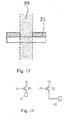
- the term "gap space” indicates a gap between adjacent driving electrodes 51 and all spaces vertically above and vertically under the gap (i.e., a gray region in Fig. 13 ). That is, a portion between and surrounded by adjacent driving electrodes is the gap, and the gap and its extension portion in the direction perpendicular to the substrate is the gap space.
- the auxiliary electrode capable of driving the droplet to move is disposed at the gap space between the driving electrodes.
- the auxiliary electrode and the driving electrodes are in different layers, and thus the auxiliary electrode and the driving electrodes may overlap with each other. Therefore, the driving electric field can be formed at the gap space between the driving electrodes, thereby eliminating or reducing the space where the driving electric field cannot be formed, and controlling the droplet more smoothly.
- the present embodiment provides a micro-fluidic substrate, which includes:
- the substrate 8 is a substrate for carrying other structures, and may have a plate shape.
- the plurality of driving electrodes 51 are disposed in a same layer and arranged in an array (e.g., a rectangular array), and are configured to apply a driving voltage to drive the droplet 9 to move. It is noted that, since the driving electrodes 51 are disposed in the same layer with a gap space provided therebetween, the driving electrodes 51 cannot contact each other, so as to ensure that different driving electrodes 51 are insulated from each other.
- the auxiliary electrode 6 is further provided in the gap space 59 between the driving electrodes 51.
- the auxiliary electrode 6 is disposed on a side of the substrate 8 provided with the driving electrodes 51.
- the auxiliary electrode 6 can also be applied with the driving voltage to drive the droplet 9 to move, thereby eliminating or reducing the space where the driving electric field cannot be formed, and controlling the droplet 9 more smoothly.
- an orthographic projection of the auxiliary electrode 6 on the substrate 8 at least covers an orthographic projection of the gap space 59 on the substrate 8.
- the orthographic projection of the auxiliary electrode 6 on the substrate 8 coincides with the orthographic projection of the gap space 59 on the substrate 8.
- the auxiliary electrode 6 and the driving electrodes 51 are in different layers, and therefore, different driving electrodes 51 will be not electrically connected with each other even if the orthographic projection of the auxiliary electrode 6 on the substrate overlaps with the orthographic projection of the driving electrodes 51 on the substrate 8.
- the auxiliary electrode 6 e.g., a first auxiliary electrode 61 and a second auxiliary electrode 62 described later
- the gap space 59 e.g., a row gap space 591 and a column gap space 592 described later
- the auxiliary electrode 6 may extend beyond the gap space 59, referring to Fig. 6 , to completely eliminate the space where the driving electric field cannot be formed.
- the orthographic projection of the auxiliary electrode 6 on the substrate 8 may completely overlap with the orthographic projection of the gap space 59 where the auxiliary electrode 6 is located.
- the auxiliary electrode 6 is disposed on the side of the driving electrodes 51 away from the substrate 8.
- the auxiliary electrode 6 and the driving electrodes 51 when the auxiliary electrode 6 and the driving electrodes 51 are disposed on the same side of the substrate 8, the auxiliary electrode 6 can be farther away from the substrate 8 than the driving electrodes 51, so that the process for fabricating the structure related to the driving electrodes 51 does not need to be changed, and the process can be easily implemented by adding a step of fabricating the auxiliary electrode 6 after the driving electrodes 51 are fabricated.
- the auxiliary electrode 6 may be made of a metal material.
- the driving electrodes 51 are arranged in an array, with a row gap space 591 between adjacent rows of driving electrodes 51 and a column gap space 592 between adjacent columns of driving electrodes 51.
- the auxiliary electrode 6 includes a first auxiliary electrode 61 at least partially disposed in the row gap space 591 and having a strip shape, and a second auxiliary electrode 62 at least partially disposed in the column gap space 592 and having a strip shape, the second auxiliary electrode 62 being insulated from the first auxiliary electrode 61.
- the driving electrodes 51 are usually disposed in a matrix in a plurality of rows and columns, so that a plurality of "row gap spaces 591" extending in a row direction and a plurality of "column gap spaces 592" extending in the column direction may be formed therein, and the auxiliary electrodes 6 may include first auxiliary electrodes 61 arranged along the row gap spaces 591 and second auxiliary electrodes 62 arranged along the column gap spaces 592.
- the first auxiliary electrodes 61 and the second auxiliary electrodes 62 are insulated to avoid signal interference therebetween.
- each row gap space 591 is provided with one first auxiliary electrode 61 having a strip shape
- each column gap space 592 is provided with one second auxiliary electrode 62 having a strip shape.
- the first auxiliary electrodes 61 may be disposed in all of the row gap spaces 591, there is only one first auxiliary electrode 61 in each row gap space 591, and the one first auxiliary electrode 61 fills the row gap space 591; similarly, there is only one second auxiliary electrode 62 in each column gap space 592 and the one second auxiliary electrode 62 fills the column gap space 592.
- the auxiliary electrode 6 completely occupies the space of the gap space 59 when viewed in a plan view. In this way, all of the gap spaces 51 may be filled with the auxiliary electrodes 6, thereby completely eliminating the space where the driving electric field cannot be formed, and improving the driving accuracy.
- auxiliary electrode 6 Since only one auxiliary electrode 6 is provided in each gap space 59, the total number of auxiliary electrodes 6 is not too large, which facilitates the control thereof. For example, a signal can be directly provided to one auxiliary electrode 6 through each port of a driving chip (IC).
- IC driving chip
- the second auxiliary electrode 62 and the first auxiliary electrode 61 are in different layers with an overlap therebetween, and an insulating layer is disposed between the second auxiliary electrode 62 and the first auxiliary electrode 61 at least at the overlap.
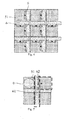
- first auxiliary electrode 61 and the second auxiliary electrode 62 fill the row gap space 591 and the column gap space 592, respectively, they must overlap, as shown in Fig. 2 , at the intersection of the row gap space 591 and the column gap space 592.
- the first auxiliary electrode 61 and the second auxiliary electrode 62 may be in different layers, and as shown in Fig. 5 , they may be separated by an insulating layer (e.g., a fourth passivation layer 808) at the overlap.
- the micro-fluidic substrate further includes a plurality of first gate lines 31 extending in the row direction, a plurality of driving lines 41 extending in the column direction, and a plurality of driving transistors D1.
- each of the driving electrodes 51 and each of the driving transistors D1 are disposed between adjacent first gate lines 31 and between adjacent driving lines 41.
- the driving transistor D1 is configured to control the driving voltage applied to the driving electrode 51 to drive the droplet 9 on the driving electrode to move.
- the driving electrode 51 corresponds to the driving transistor D1 that controls the driving electrode 51.
- the driving electrodes 51 are arranged in an array, with a row gap space 591 between adjacent rows of the driving electrodes 51 and a column gap space 592 between adjacent columns of the driving electrodes 51.
- each driving electrode 51 is coupled to a first electrode of the driving transistor D1 corresponding thereto, gate electrodes of respective driving transistors D1 corresponding to each row of driving electrodes 51 are coupled to one of the first gate lines 31, and second electrodes of respective driving transistors D1 corresponding to each column of driving electrodes 51 are coupled to one of the driving lines 41.
- the driving electrodes 51 since the number of the driving electrodes 51 is large, they can be controlled by a transistor array. That is, a turn-on signal is provided to respective first gate lines 31 in turn, so that respective rows of the driving transistors D1 are turned on in turn. When a certain row of the driving transistors D1 are turned on, driving voltages can be provided to the row of respective driving electrodes 51 through respective driving lines 41. Thus, a large number of driving electrodes 51 can be controlled with a few lead wires.
- the auxiliary electrode 6 includes the first auxiliary electrode 61 and the second auxiliary electrode 62.
- the first gate line 31 is disposed in the row gap space 591
- the first auxiliary electrode 61 is also disposed in the row gap space 591 where the first gate line 31 is disposed
- the first auxiliary electrode 61 is on a side of the first gate line 31 away from the substrate 8 (see Fig. 3 ).
- the driving line 41 is disposed in the column gap space 592
- the second auxiliary electrode 62 is disposed in the column gap space 592 where the driving line 41 is disposed, and the second auxiliary electrode 62 is located on a side of the driving line 41 away from the substrate 8 (see Fig. 4 ).
- the first gate line 31, the driving line 41, the first auxiliary electrode 61 and the second auxiliary electrode 62 may be disposed on the same side of the substrate, as shown in Figs. 2 , 3 and 4 , the first gate line 31 and the driving line 41 may also be respectively in the row gap space 591 and the column gap space 592.
- the corresponding first auxiliary electrode 61 and the corresponding second auxiliary electrode 62 are respectively above the first gate line 31 and the driving line 41, so as to shield the signals in the first gate line 31 and the driving line 41 from affecting the droplet 9.
- the auxiliary electrodes 6 each have block shape, and each auxiliary electrode 6 is located in the gap space 59 between two adjacent driving electrodes 51 and is electrically coupled to one driving electrode 51 adjacent thereto.
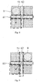
- the auxiliary electrode 6 may not have a shape of strip, but may have a shape of "small block", and each auxiliary electrode 6 is only located between two adjacent driving electrodes 51, and at the same time, the auxiliary electrode 6 is also electrically coupled to one of the driving electrodes 51 adjacent to the auxiliary electrode (for example, electrically coupled through a via hole penetrating through an insulating layer between the auxiliary electrode 6 and the one driving electrode 51, and a black dot in Fig. 6 represents a via hole), so that the signal via the auxiliary electrode 6 is the same as the signal via the one driving electrode 51.
- the driving electrode 51 is "expanded" into the gap space 59, and thus, the space where the driving electric field cannot be formed can be reduced.
- respective sides of one driving electrode 51 are provided with the gap spaces 59.
- the auxiliary electrodes 6 having a block shape may be provided in each of the gap spaces 59, or only some of the gap spaces 59 are provided with the auxiliary electrode 6, or none of the gap spaces 59 provided with the auxiliary electrode 6.
- Each of the driving electrodes 51 may be coupled to only one auxiliary electrode 6 adjacent thereto, may be coupled to a plurality of auxiliary electrodes 6, or may not be coupled to any of the auxiliary electrodes 6.
- each driving electrode 51 is coupled to the auxiliary electrodes 6 at gap spaces 59 on the same side of the driving electrode 51.
- each of the driving electrodes 51 may be coupled to the auxiliary electrodes 6 on the right and upper sides thereof, as shown in Fig. 6 .
- the micro-fluidic substrate further includes a plurality of photosensitive elements D3 on the substrate 8.
- the concentration, composition, etc. of the droplet 9 need to be detected, which can be implemented by setting the photosensitive element D3 (which may be disposed on a side of the substrate 8 provided with the driving electrodes 51), and therefore the photosensitive element D3 may be disposed on the substrate 8.
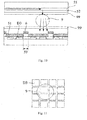
- Fig. 10 for simplicity, part of the structure is not shown in the figure
- light can be transmitted to the substrate 8 of the micro-fluidic substrate through an optical waveguide layer 55 and the like provided on the counter substrate.
- parameters such as the intensities of light passing through the droplet 9 and light not passing through the droplet 9 are different, as shown in Fig. 11 , it can be determined which photosensitive elements D3 have the droplet 9 above them by analyzing the light detected by each photosensitive element D3, that is, the positioning of the droplet 9 can be achieved.
- the detection of the concentration, composition, and the like of the droplets 9 can be achieved by analyzing the light detected by the photosensitive element D3.
- the photosensitive element D3 may be a photodiode or the like, which will not be described in detail herein.
- the photosensitive elements D3 may be in one-to-one correspondence with the driving electrodes 51 as shown in Fig. 2 .
- the number of the photosensitive elements D3 and the number of the driving electrodes 51 may be different.
- the orthographic projection of the photosensitive element D3 on the substrate 8 is covered by the orthographic projection of the driving electrode 51 on the substrate 8; the driving electrode 51 is on the side of the photosensitive element D3 away from the substrate 8, and is made of a transparent conductive material.
- the photosensitive element D3 only needs to receive light without causing an electric field, and thus, as shown in Figs. 2 and 3 , it may be disposed under the driving electrodes 51 (in this case, the driving electrodes 51 are transparent), so that the area of the driving electrodes 51 is not reduced, and the electric field caused by the driving electrodes 51 is not affected.
- the micro-fluidic substrate further includes a plurality of second gate lines 32 extending in the row direction, a plurality of detection lines 42 extending in the column direction, and a plurality of detection transistors D2 corresponding to the photosensitive elements D3 in one-to-one correspondence.
- each photosensitive element D3 is coupled to a first electrode of detection transistor D2 corresponding thereto, gate electrodes of respective detection transistors D2 corresponding to each row of photosensitive elements D3 are coupled to one second gate line 32, and second electrodes of respective detection transistors D2 corresponding to each column of photosensitive elements D3 are coupled to one detection line 42.
- the photosensitive elements D3 may also be controlled by a transistor array (where the second gate line 32 and the detection line 42 may or may not be in the gap space 59).
- a turn-on signal is provided through one of the second gate lines 32, a corresponding row of the detection transistors D2 are turned on, so that the light intensity signals detected by the photosensitive elements D3 in the corresponding row can be respectively output through the corresponding detection lines 42.
- many structures may be disposed in the same layer.
- the second gate line 32 and the first gate line 31 may be disposed in the same layer
- the gate electrodes of the detection transistor D2 and the driving transistor D1 may be disposed in the same layer as the second gate line 32 and the first gate line
- the source electrodes and the drain electrodes of the detection transistor D2 and the driving transistor D1 may be disposed in the same layer
- the driving line 41 and the detection line 42 may be disposed in the same layer.
- the micro-fluidic substrate may further have other desired structures, such as an insulating layer for separating different conductive structures, a planarization layer (or resin layer) for eliminating a step difference, a lyophobic layer 99 on the uppermost layer, and the like.
- other desired structures such as an insulating layer for separating different conductive structures, a planarization layer (or resin layer) for eliminating a step difference, a lyophobic layer 99 on the uppermost layer, and the like.
- a method of fabricating a micro-fluidic substrate may include steps S01 to S20.
- Step S01 includes forming a first gate line 31, a second gate line 32, and gate electrodes of a detection transistor D2 and a driving transistor D1 on a substrate 8.
- Step S02 includes forming a gate insulating layer 801 of the detection transistor D2 and the driving transistor D1.
- the gate insulating layer 801 covers the first gate line 31, the second gate line 32, and the gate electrodes of the detection transistor D2 and the driving transistor D1, and the first gate line 31, the second gate line 32, and the gate electrodes of the detection transistor D2 and the driving transistor D1 are spaced apart from each other by the gate insulating layer 801.
- Step S03 includes forming active regions of the detection transistor D2 and the driving transistor D1 on the gate insulating layer 801.
- Step S04 includes forming source electrodes and drain electrodes of the detection transistor D2 and the driving transistor D1, the driving line 41 and the detection line 42 on the gate insulating layer 801.
- Step S05 includes forming a first passivation layer (PVX) 802, and the first passivation layer 802 covers the source electrodes and the drain electrodes of the detection transistor D2 and the driving transistor D1, the driving line 41, and the detection line 42 and insulates them from each other.
- PVX first passivation layer
- Step S06 includes etching the first passivation layer 802 to expose a first electrode (which may be a source electrode or a drain electrode) of the detection transistor D2 and a first electrode (which may be a source electrode or a drain electrode) of the driving transistor D1.
- Step S06 further includes forming an anode of a photodiode (an example of the photosensitive element D3) on the first electrode of the detection transistor D2 and forming a first connection structure CT1 for assisting the connection between the driving electrode 51 and the driving transistor D1 on the first electrode of the driving transistor D1.
- the anode and the first connection structure CT1 are, for example, portions defined by thick solid lines in Fig. 3 and may be made of metal materials.
- Step S07 includes forming a semiconductor layer of the photodiode on the anode.
- the photodiode may be a PIN photodiode.
- Step S08 includes forming a cap layer of the photodiode on the semiconductor layer, which may be made of transparent conductive material such as Indium Tin Oxide (ITO).
- ITO Indium Tin Oxide
- Step S09 includes forming a cover layer 803 to cover the photodiode and the first passivation layer.
- Step S10 includes forming a first resin layer 804 cover the cover layer 803.
- Step S11 includes forming a second passivation layer 805 to cover the first resin layer 804.
- the formation of the second passivation layer 805 may include processes such as etching and deposition, which will not be described in detail herein.
- Step S12 includes forming a cathode of the photodiode and a lead wire for supplying power thereto, while forming a second connection structure CT2 for assisting the connection between the driving electrode 51 and the driving transistor D1.
- the formation of the second connection structure CT2 may include a process such as deposition.
- Step S13 includes forming a barrier layer 806 on a portion of the second passivation layer 805 not covered by the second connection structure CT2.
- Step S14 includes forming driving electrodes 51 spaced apart from each other on the barrier layer 806 and the second connection structure CT 2.
- Step S15 includes forming a third passivation layer 807, the third passivation layer 807 covering the driving electrodes 51 and insulating the driving electrodes 51 from each other.
- Step S16 includes forming a first auxiliary electrode 61 on the third passivation layer 807.
- Step S17 includes forming a fourth passivation layer 808 on the third passivation layer 807 and the first auxiliary electrode 61, the fourth passivation layer 808 serving as the insulating layer for separating the first auxiliary electrode 61 from the second auxiliary electrode 62 as described above.
- Step S18 includes forming the second auxiliary electrode 62 on the fourth passivation layer 808 (see Fig. 4 ).
- Step S19 includes forming a second resin layer 809 to cover the second auxiliary electrode 62.
- Step S20 includes forming a lyophobic layer 99 on the second resin layer 809.
- each transistor can also be a top-gate structure.
- the positions of the layers in which the first auxiliary electrode 61 and the second auxiliary electrode 62 are located can be interchanged, and the details thereof will not be described herein.
- a lead wire for connecting the auxiliary electrode 6 e.g., a lead wire 621 for connecting the second auxiliary electrode 62 may be formed.
- the present embodiment provides a micro-fluidic structure, which includes: a micro-fluidic substrate according to an embodiment of the present disclosure; and a counter substrate opposite to the micro-fluidic substrate.
- a side of the micro-fluidic substrate provided with the driving electrodes 51 faces the counter substrate, a side of the counter substrate facing the micro-fluidic substrate is provided with a common electrode facing each of the driving electrodes 51, and a space for accommodating the droplet 9 is between the micro-fluidic substrate and the counter substrate.
- the above micro-fluidic substrate and the counter substrate can be disposed opposite to each other to form a micro-fluidic structure, in which the counter substrate has the common electrode 52, so that a required driving electric field can be formed between the two substrates to drive the droplet 9 therebetween to move.
- a lyophobic layer 99 is disposed on a side of the micro-fluidic substrate closest to the counter substrate; and a lyophobic layer 99 is disposed on a side of the counter substrate closest to the micro-fluidic substrate.
- the lyophobic layers 99 i.e., layers having liquid repellency to the droplet 9 are provided on the opposite sides of the above two substrates so that a predetermined contact angle can be formed between the lyophobic layers 99 and the droplet 9 contacting them, which facilitates the movement of the droplet.
- the lyophobic layers 99 may be made of a material such as teflon.
- the counter substrate when the micro-fluidic substrate is a micro-fluidic substrate having a photosensitive element D3, the counter substrate further includes an optical waveguide layer 55 for guiding and directing light towards the micro-fluidic substrate.
- a corresponding optical waveguide layer 55 may be disposed in the counter substrate to guide light incident from a right or left side and direct the light toward the micro-fluidic substrate.
- the optical waveguide layer may not be provided, and the light may be emitted toward the micro-fluidic substrate by a light source located on a side of the transparent counter substrate away from the micro-fluidic substrate.
- the present embodiment provides a method for driving a micro-fluidic structure, including: applying a common voltage to the common electrode 52, applying a driving voltage to the driving electrode 51 at a first position, and applying the driving voltage to the auxiliary electrode 6 at a second position to form a driving electric field to drive the droplet 9 to move, wherein the first position represents a position of the driving electrode 51 to which the droplet 9 is to be moved in a moving direction of the droplet 9, and the second position represents a position of the auxiliary electrode to which the droplet 9 is to be moved in the moving direction of the droplet 9.
- the auxiliary electrode 6 is provided, if there is an auxiliary electrode 6 at least a part of which is located at the position where the droplet is expected to reach, the driving voltage may be applied to the auxiliary electrode 6 to assist driving of the droplet 9, in addition to applying the driving voltage to the driving electrode 51 located at the position where the droplet is expected to reach.
- the same driving voltage as that applied to the driving electrode 51 at the first position may be applied to the auxiliary electrode 6 through the lead wire coupled to the auxiliary electrode 6 at the second position (as shown in Fig. 2 , the lead wire 621 coupled to the second auxiliary electrode 62).
- the auxiliary electrode 6 has a block shape as shown in Fig. 6
- the same driving voltage as that applied to the driving electrode 51 may be applied to the auxiliary electrode 6.
- a high voltage may be applied to the second auxiliary electrode 62 and the driving electrode 51 on the right side thereof (marked by a dashed line frame in the figure).
- a high voltage may be applied to the first auxiliary electrode 61 and the driving electrode 51 on the lower side thereof (marked by a dashed line frame in the figure).
- a high voltage may be applied to the first auxiliary electrode 61 on the lower side thereof, the second auxiliary electrode 62 on the left side thereof, and the driving electrode 51 on the lower left side thereof (marked by the dashed line in the figure).
- each auxiliary electrode 6 may be directly coupled to a driving chip (IC), so that they may be directly supplied with a driving voltage by the driving chip.
- IC driving chip
- the voltage on the auxiliary electrode 6 is supplied through the driving electrode 51 coupled thereto.
- the driving voltage applied to the auxiliary electrode 6 is equal to the driving voltage applied to at least one driving electrode 51 adjacent to the auxiliary electrode 6.
- the auxiliary electrode 6 can be regarded as an extension of the driving electrode 51, so the driving voltage on the auxiliary electrode 6 may be equal to the driving voltage of a certain driving electrode 51 that is also being driven.
- the driving voltage applied to the auxiliary electrode 6 may be different from the driving voltages applied to the driving electrodes 51, for example, the driving voltages applied to the driving electrodes may be varied, and the specific driving voltages thereto may be obtained according to the driving requirement for the droplet 9, and will not be described in detail herein.
Landscapes
- Chemical & Material Sciences (AREA)
- Health & Medical Sciences (AREA)
- Dispersion Chemistry (AREA)
- Analytical Chemistry (AREA)
- General Health & Medical Sciences (AREA)
- Hematology (AREA)
- Clinical Laboratory Science (AREA)
- Chemical Kinetics & Catalysis (AREA)
- Micromachines (AREA)
- Physical Or Chemical Processes And Apparatus (AREA)
- Automatic Analysis And Handling Materials Therefor (AREA)
Applications Claiming Priority (2)
| Application Number | Priority Date | Filing Date | Title |
|---|---|---|---|
| CN201810866305.9A CN110787843B (zh) | 2018-08-01 | 2018-08-01 | 微流控基板、微流控结构及其驱动方法 |
| PCT/CN2019/097548 WO2020024860A1 (fr) | 2018-08-01 | 2019-07-24 | Substrat microfluidique, structure microfluidique et procédé de commande correspondant |
Publications (2)
| Publication Number | Publication Date |
|---|---|
| EP3831480A1 true EP3831480A1 (fr) | 2021-06-09 |
| EP3831480A4 EP3831480A4 (fr) | 2022-04-06 |
Family
ID=69231423
Family Applications (1)
| Application Number | Title | Priority Date | Filing Date |
|---|---|---|---|
| EP19843941.6A Pending EP3831480A4 (fr) | 2018-08-01 | 2019-07-24 | Substrat microfluidique, structure microfluidique et procédé de commande correspondant |
Country Status (4)
| Country | Link |
|---|---|
| US (3) | US11331666B2 (fr) |
| EP (1) | EP3831480A4 (fr) |
| CN (1) | CN110787843B (fr) |
| WO (1) | WO2020024860A1 (fr) |
Families Citing this family (4)
| Publication number | Priority date | Publication date | Assignee | Title |
|---|---|---|---|---|
| EP4186593A4 (fr) * | 2020-12-25 | 2023-12-27 | BOE Technology Group Co., Ltd. | Substrat pour entraînement de gouttelettes et son procédé de fabrication, et dispositif microfluidique |
| CN115245844B (zh) * | 2021-04-27 | 2025-01-10 | 上海天马微电子有限公司 | 一种微流控芯片 |
| CN116899640B (zh) * | 2022-09-29 | 2025-12-05 | 成都天马微电子有限公司 | 微流控装置的驱动方法及微流控装置 |
| CN119968062B (zh) * | 2025-04-10 | 2025-10-03 | 惠科股份有限公司 | 显示模组及其制备方法 |
Family Cites Families (9)
| Publication number | Priority date | Publication date | Assignee | Title |
|---|---|---|---|---|
| TWI303312B (en) * | 2005-12-21 | 2008-11-21 | Ind Tech Res Inst | Matrix electrodes controlling device and digital fluid detection platform thereof |
| CN101679078B (zh) * | 2007-05-24 | 2013-04-03 | 数字化生物系统 | 基于电湿润的数字微流体 |
| CN102866193B (zh) * | 2012-09-04 | 2015-04-01 | 吴传勇 | 基于介电泳来操控液体中的粒子的器件及方法 |
| CN103386332A (zh) * | 2013-07-09 | 2013-11-13 | 苏州大学 | 微流控芯片输运液滴的方法 |
| TWI507690B (zh) * | 2014-09-02 | 2015-11-11 | Silicon Optronics Inc | 生物晶片構裝 |
| WO2018093779A2 (fr) * | 2016-11-18 | 2018-05-24 | Digital Biosystems | Dispositifs microfluidiques numériques |
| CN107649223B (zh) * | 2017-09-27 | 2019-10-15 | 京东方科技集团股份有限公司 | 液滴控制检测器件及其工作方法 |
| CN109465041B (zh) * | 2018-11-12 | 2021-04-27 | 京东方科技集团股份有限公司 | 微流控装置、微流控装置的控制方法及微全分析系统 |
| CN110069168B (zh) * | 2019-05-05 | 2022-09-30 | 京东方科技集团股份有限公司 | 微流控装置、用于微流控装置的操作方法及控制装置 |
-
2018
- 2018-08-01 CN CN201810866305.9A patent/CN110787843B/zh active Active
-
2019
- 2019-07-24 WO PCT/CN2019/097548 patent/WO2020024860A1/fr not_active Ceased
- 2019-07-24 EP EP19843941.6A patent/EP3831480A4/fr active Pending
- 2019-07-24 US US16/633,016 patent/US11331666B2/en active Active
-
2022
- 2022-04-21 US US17/726,119 patent/US12017219B2/en active Active
-
2024
- 2024-05-15 US US18/664,880 patent/US12251699B2/en active Active
Also Published As
| Publication number | Publication date |
|---|---|
| US20210060547A1 (en) | 2021-03-04 |
| US20220241778A1 (en) | 2022-08-04 |
| US11331666B2 (en) | 2022-05-17 |
| CN110787843B (zh) | 2021-03-23 |
| US20240293813A1 (en) | 2024-09-05 |
| US12017219B2 (en) | 2024-06-25 |
| EP3831480A4 (fr) | 2022-04-06 |
| US12251699B2 (en) | 2025-03-18 |
| CN110787843A (zh) | 2020-02-14 |
| WO2020024860A1 (fr) | 2020-02-06 |
Similar Documents
| Publication | Publication Date | Title |
|---|---|---|
| US12251699B2 (en) | Micro-fluidic substrate, micro-fluidic structure and driving method thereof | |
| CN109174219B (zh) | 微流控基板及其驱动方法和微流控装置 | |
| US11107839B2 (en) | Array substrate and manufacturing method thereof, and display panel | |
| EP3989288B1 (fr) | Substrat de réseau, écran d'affichage et appareil d'affichage | |
| US11534762B2 (en) | Microfluidic device, method of using microfluidic device and micro total analysis system | |
| US12096656B2 (en) | Array substrate and manufacturing method thereof, and display panel | |
| US20180203565A1 (en) | Touch control display device and manufacturing method thereof | |
| CN119500300B (zh) | 一种微流控芯片 | |
| US11782549B2 (en) | Display panel and display device | |
| CN108169966B (zh) | 液滴控制检测器件及液滴控制检测方法 | |
| US11691147B2 (en) | Digital microfluidic chip and digital microfluidic system | |
| CN104851789B (zh) | 薄膜晶体管及制作方法、阵列基板及制作方法和显示装置 | |
| KR101891346B1 (ko) | 전기습윤 표시장치용 화소구조 및 그 제조방법 | |
| US10910411B2 (en) | Array substrate, manufacturing method thereof and display panel | |
| US20240091766A1 (en) | Microfluidic device | |
| US20260013287A1 (en) | Microfluidic transfer substrate and method for transferring light-emitting elements | |
| CN115722282A (zh) | 微流控基板、微流控装置及其驱动方法 | |
| CN107797344A (zh) | 阵列基板、显示面板及其制造方法 | |
| US12376482B2 (en) | Stretchable substrate and stretchable display device | |
| WO2020211547A1 (fr) | Substrat microfluidique numérique et puce microfluidique numérique | |
| US20230422550A1 (en) | Display device | |
| US12464916B2 (en) | Display panel with metal oxide layer | |
| CN114284301A (zh) | 显示面板及移动终端 | |
| WO2020211533A1 (fr) | Substrat microfluidique numérique, son procédé de fabrication, et puce microfluidique numérique | |
| US20250290809A1 (en) | Detection device |
Legal Events
| Date | Code | Title | Description |
|---|---|---|---|
| STAA | Information on the status of an ep patent application or granted ep patent |
Free format text: STATUS: THE INTERNATIONAL PUBLICATION HAS BEEN MADE |
|
| PUAI | Public reference made under article 153(3) epc to a published international application that has entered the european phase |
Free format text: ORIGINAL CODE: 0009012 |
|
| STAA | Information on the status of an ep patent application or granted ep patent |
Free format text: STATUS: REQUEST FOR EXAMINATION WAS MADE |
|
| 17P | Request for examination filed |
Effective date: 20200522 |
|
| AK | Designated contracting states |
Kind code of ref document: A1 Designated state(s): AL AT BE BG CH CY CZ DE DK EE ES FI FR GB GR HR HU IE IS IT LI LT LU LV MC MK MT NL NO PL PT RO RS SE SI SK SM TR |
|
| DAV | Request for validation of the european patent (deleted) | ||
| DAX | Request for extension of the european patent (deleted) | ||
| A4 | Supplementary search report drawn up and despatched |
Effective date: 20220310 |
|
| RIC1 | Information provided on ipc code assigned before grant |
Ipc: B01L 3/00 20060101AFI20220303BHEP |
|
| STAA | Information on the status of an ep patent application or granted ep patent |
Free format text: STATUS: EXAMINATION IS IN PROGRESS |
|
| 17Q | First examination report despatched |
Effective date: 20250703 |