EP3832201A1 - Optische vorrichtung zur steuerung von licht aus einer externen lichtquelle - Google Patents
Optische vorrichtung zur steuerung von licht aus einer externen lichtquelle Download PDFInfo
- Publication number
- EP3832201A1 EP3832201A1 EP19425085.8A EP19425085A EP3832201A1 EP 3832201 A1 EP3832201 A1 EP 3832201A1 EP 19425085 A EP19425085 A EP 19425085A EP 3832201 A1 EP3832201 A1 EP 3832201A1
- Authority
- EP
- European Patent Office
- Prior art keywords
- optical
- light
- waveguide
- optical device
- light emitting
- Prior art date
- Legal status (The legal status is an assumption and is not a legal conclusion. Google has not performed a legal analysis and makes no representation as to the accuracy of the status listed.)
- Granted
Links
Images



Classifications
-
- G—PHYSICS
- G02—OPTICS
- G02B—OPTICAL ELEMENTS, SYSTEMS OR APPARATUS
- G02B6/00—Light guides; Structural details of arrangements comprising light guides and other optical elements, e.g. couplings
- G02B6/0001—Light guides; Structural details of arrangements comprising light guides and other optical elements, e.g. couplings specially adapted for lighting devices or systems
- G02B6/0011—Light guides; Structural details of arrangements comprising light guides and other optical elements, e.g. couplings specially adapted for lighting devices or systems the light guides being planar or of plate-like form
- G02B6/0033—Means for improving the coupling-out of light from the light guide
- G02B6/0035—Means for improving the coupling-out of light from the light guide provided on the surface of the light guide or in the bulk of it
- G02B6/0036—2-D arrangement of prisms, protrusions, indentations or roughened surfaces
-
- G—PHYSICS
- G02—OPTICS
- G02B—OPTICAL ELEMENTS, SYSTEMS OR APPARATUS
- G02B6/00—Light guides; Structural details of arrangements comprising light guides and other optical elements, e.g. couplings
- G02B6/0001—Light guides; Structural details of arrangements comprising light guides and other optical elements, e.g. couplings specially adapted for lighting devices or systems
- G02B6/0011—Light guides; Structural details of arrangements comprising light guides and other optical elements, e.g. couplings specially adapted for lighting devices or systems the light guides being planar or of plate-like form
- G02B6/0075—Arrangements of multiple light guides
-
- G—PHYSICS
- G02—OPTICS
- G02B—OPTICAL ELEMENTS, SYSTEMS OR APPARATUS
- G02B6/00—Light guides; Structural details of arrangements comprising light guides and other optical elements, e.g. couplings
- G02B6/10—Light guides; Structural details of arrangements comprising light guides and other optical elements, e.g. couplings of the optical waveguide type
- G02B6/12—Light guides; Structural details of arrangements comprising light guides and other optical elements, e.g. couplings of the optical waveguide type of the integrated circuit kind
- G02B6/12002—Three-dimensional structures
-
- G—PHYSICS
- G02—OPTICS
- G02B—OPTICAL ELEMENTS, SYSTEMS OR APPARATUS
- G02B6/00—Light guides; Structural details of arrangements comprising light guides and other optical elements, e.g. couplings
- G02B6/10—Light guides; Structural details of arrangements comprising light guides and other optical elements, e.g. couplings of the optical waveguide type
- G02B6/12—Light guides; Structural details of arrangements comprising light guides and other optical elements, e.g. couplings of the optical waveguide type of the integrated circuit kind
- G02B2006/12133—Functions
- G02B2006/12159—Interferometer
-
- G—PHYSICS
- G03—PHOTOGRAPHY; CINEMATOGRAPHY; ANALOGOUS TECHNIQUES USING WAVES OTHER THAN OPTICAL WAVES; ELECTROGRAPHY; HOLOGRAPHY
- G03H—HOLOGRAPHIC PROCESSES OR APPARATUS
- G03H1/00—Holographic processes or apparatus using light, infrared or ultraviolet waves for obtaining holograms or for obtaining an image from them; Details peculiar thereto
- G03H1/0005—Adaptation of holography to specific applications
Definitions
- the invention relates to an optical device for controlling light from an external light source comprising at least a first and a second waveguide for guiding a light beam emitted from the external light source, and at least a first beam shaping structure with a first light emitting area for emitting a light beam and a second beam shaping structure with a second light emitting area for emitting a light beam, wherein the first waveguide guides the light beam emitted from the external light source to the first beam shaping structure and the second waveguide guides the light beam emitted from the external light source to the second beam shaping structure.
- Some optical devices are known that distribute coherent light over a larger area. This is for example necessary for backlight units of holographic displays.
- Holographic displays are able to essentially faithfully recreate the light field emitted by an object and hence become visually indistinguishable from it. They have substantial advantages over e.g. (auto-)stereoscopic displays, which provide one image per eye and thus introduce a sense of three-dimensionality, but encounter a fundamental problem: since the brain perceives a three-dimensional (3D) scene, the eye should be able to focus on arbitrary parts within it, but only one focus-plane of the scenery can be shown by the display. This mismatch causes visual fatigue and nausea, which is a major problem and one of the factors prohibiting the widespread adoption of 3D displays. Holographic displays avoid this problem and the image created appears completely natural to the eye.
- SLMs spatial light modulators
- transmissive SLMs which work analogously to liquid crystal displays
- reflective SLMs i.e. liquid crystal on silicon (LCOS) and/or' digital light processing (DLP)
- DLP digital light processing
- SLM and LCOS are compact and suitable for use in e.g. head-mounted holographic goggles.
- holographic volume gratings are also susceptible to both temperature and humidity changes, causing changes in the emitted wavefront and hence a reduction of the holographic image quality which can also not be sufficiently compensated for due to the same reasons. Furthermore, the efficiency of holographic gratings is still a major challenge.
- Backlight units for conventional displays i.e. producing a non-coherent backlighting
- US 2013/0308339 A1 discloses a light guiding valve apparatus with a transparent slab.
- the light emitted from a (coherent or non-coherent) light source spreads out in the slab acting as a single waveguide and is reflected at its surfaces.
- the transparent slab includes a stepped back surface which acts to emit the light from a front surface of the transparent slab.
- light leaving the front surface at one point can have taken a multitude of different optical paths within the slab, such that the emitted light cannot be coherent and its phases are not well-defined.
- the light is not emitted homogeneously over the front surface.
- This apparatus is therefore not suitable for example as a backlight unit for a holographic display.
- US 9,395,690 B2 shows a holographic display with an illumination device, an enlarging unit and a light modulator.
- the illumination device includes at least one light source and a light collimation unit.
- the light collimation unit collimates the light of the at least one light source.
- a cascade of fibre optic switches in the light collimation unit allows to illuminate lenses of a collimation lens array.
- the collimation lens array can comprise cylindrical lenses. However, this does not allow a compact design.
- the subsequent use of transmissive volume gratings further reduces the well-definedness of the phases on being emitted and in connection with this also the stability to changes in ambient conditions, e.g. ambient temperature. Therefore, it does not provide a stable coherent light homogeneity over some area.
- optical devices that are known are suitable for a compact, in particular flat, and reliable holographic display.
- optical devices that distribute coherent light over a larger area are also required for other applications, such as structured light sensing (3D sensing) or LIDAR.
- the efficiency of the optical device is also a very important aspect for these applications and is, additionally to the other points, not sufficiently achieved by the present optical devices.
- a compact way means that the optical device shall allow such illumination of the area, while having reduced dimensions normal to that area compared to a solution covering the same area essentially with a single beam shaping structure (e.g. a single set of lenses).
- an optical device for controlling light from an external light source as mentioned in the outset, wherein the first and the second beam shaping structure are each configured such that the uniformity of the radiant density and/or intensity profile of a light beam emitted from a respective light emitting area of the respective beam shaping structure is higher than that of the light beam guided to the respective beam shaping structure by the respective waveguide.
- the present disclosure generally avoids mixing between the two or more optical paths used for covering the total light emitting area.
- the device is relatively insensitive to temperature changes and resulting deformations, maintaining coherence in each optical path individually.
- the phase of the light at points in the area can be well-defined or is easily determinable, in particular in dependence on a temperature of the optical device or an ambient temperature.
- such a setup with at least a first and a second waveguide, wherein each of the first and second waveguides guides light to a beam shaping structure as defined above and is associated with one of the waveguides allows for a more compact optical device compared to e.g. a single lens expanding a beam to a large diameter.
- the influence of the beam shaping structure should manipulate the beam shape such that it becomes more similar to a top-hat beam shape.
- the beam uniformity (U ⁇ ) as defined in ISO 13694:2018 for cw-beams, wherein ⁇ is 0.3 and lower (i.e. closer to 0) U ⁇ means higher beam uniformity. Therefore, the uniformity of the radiant density profile of a light beam emitted from a respective light emitting area of the respective beam shaping structure is higher than that of the light beam guided to the respective beam shaping structure by the respective waveguide means that the beam uniformity of the light beam emitted from the respective light emitting area (on being emitted from the respective light emitting area) is higher, i.e.
- U ⁇ is lower and closer to 0, than the beam uniformity of the light beam guided to the respective beam shaping structure by the respective waveguide (on leaving the respective waveguide).
- U ⁇ is optionally reduced by the influence of the beam shaping structure by at least 0.05, at least 0.1 or by at least 0.2.
- the beam uniformity is also increased (and therefore U ⁇ decreased) for ⁇ being one of 0.1, 0.2, 0.4, 0.5, 0.6 or 0.7. This measure is to be applied under the assumption that the light beam supplied by the external light source is a Gaussian beam.
- the optical device does not necessarily form a complete backlight unit, but could for example be one component of a backlight unit.
- the optical device does not necessarily need to emit plane waves, nor does the optical device necessarily comprise the external light source.
- the respective light emitting areas do not need to be physical surface areas, but could also, for example, be boundaries between different optical elements.
- the edges of the first and/or second light emitting area do not need to be structurally delimited, but they represent the area through which the light beam is emitted from the respective beam shaping structure. Furthermore, the light that is emitted from the first and/or the second light emitting area does not need to be immediately emitted from the optical device as well; however, it can be.
- the optical device comprises at least two (i.e. the first and the second) waveguides.
- the optical device comprises a number greater than two of waveguides for guiding a light beam emitted from the external light source, and a number greater than two of beam shaping structures, each of that number of beam shaping structures comprising a respective light emitting area for emitting a light beam, wherein each of the number of waveguides guides the light beam emitted from the external source to a respective one of the number of beam shaping structures, wherein each of the number of beam shaping structures is configured such that the uniformity of the radiant density profile of a light beam emitted from the respective light emitting area of the respective one of the number of beam shaping structures is higher than that of the light beam guided to the respective beam shaping structures by the respective waveguides.
- first and second beam shaping structure and/or the first and second waveguide may also apply to the number of greater than two waveguides and/or beam shaping structures and additional elements interacting with the first and second waveguide and/or first and second beam shaping structure may also interact with the number greater than two of waveguides and/or beam shaping structure in an analogous manner.
- the optical device comprises a number of at least ten waveguides, beam shaping structures and respective associated elements.
- the at least first and second waveguide may be optical waveguides and may be distinct from each other, i.e. non-overlapping.
- the first and/or the second light emitting area can be plane or flat. The first and the second light emitting area may lie in the same plane.
- the first and the second light emitting area may be adjacent to one another, i.e. less than 10% of the largest dimension of the light emitting areas distanced from one another.
- the first and the second light emitting area may be contiguous or essentially contiguous, at least in one or more directions.
- the first and/or the second light emitting area can for example have an elliptical, in particular circular, or hexagonal shape.
- the largest dimension of the first and/or the second light emitting area is preferably less than 1 mm.
- the first and the second beam shaping structure each can comprise an optical shaping element and the first and the second waveguides direct the light beam emitted from the external light source at the respective optical shaping element of the first and the second beam shaping structure, and the optical shaping elements are configured for manipulating the wavefront and/or radiant intensity distribution of the light beam directed at the respective optical shaping element.
- the manipulation is a bijective mapping and/or the light beam is manipulated such that rays of the light beam do not intersect.
- the manipulation should be such that the resulting light beam is coherent if the incoming light beam was coherent and/or such that the coherence length of the light beam is not reduced.
- the phase profile distribution and the amplitude profile distribution are manipulated in the same way.
- the respective optical shaping element is distanced from the respective light emitting area.
- the first and second waveguides direct the light beam at the respective optical shaping elements such that the light beam is directed towards the light emitting area after interfering with the respective optical shaping element.
- the optical shaping element of the first and/or the second beam shaping structure may be an optical profiler element configured to increase the uniformity of the radiant intensity (or density) profile of the light beam directed at the respective optical shaping element.
- the optical profiler elements may in particular be configured for manipulating a Gaussian beam in such a way.
- the optical profiler elements are configured for shaping a Gaussian beam into a top hat beam.
- the optical profiler elements may be diffractive optical elements (DOEs). In this way a certain area can easily be illuminated homogeneously with coherent light. Furthermore, this allows for a thin layout of the optical device.
- DOEs diffractive optical elements
- the optical shaping element of the first and/or the second beam shaping structure may be an optical diverging element configured to increase the beam divergence of the light beam directed at the respective optical diverging element.
- the optical diverging elements can be mirrors, for example micro-mirrors, in particular curved micro-mirrors, or diffractive optical elements. The optical diverging elements widen the beam divergence angle, i.e. widen the radiant intensity distribution. This allows to illuminate a larger area with one light beam emitted from the external source.
- each of the optical shaping elements is both an optical profiler element and an optical diverging element.
- the optical device may comprise an interface, wherein the first and the second light emitting area are provided by the interface.
- the first and second light emitting area can each be delimited by total internal reflection occurring outside the respective light emitting area for the light beam directed towards the interface after interfering with the respective optical shaping element. In this way, unwanted interference effects of light cones overlapping on the interface can be avoided by using total internal reflection. This allows to select only a part of the light beam/light cone to exit from the interface and the rest to be "cut-off". This "cut-off" effect can be used to select parts of the beam to be transmitted outside the light emitting area and subsequently be used for illumination purposes, while other parts are reflected at the interface.
- the external light source may emit a Gaussian-like mode, and to limit the field intensity fluctuation over the interface (and/or the light emitting surface as defined below) to 20%, only the central part within approximately a radius including 50% of the beam intensity of the light beam is used while the rest is totally internally reflected.
- the interface is provided as a front surface of a plate with a parallel back surface, the part of the light beam that experienced total internal reflection will never leave the plate through the interface and exit the plate on its side facets.
- the optical shaping elements are optical diverging elements.
- the optical shaping elements may direct the light beam at the interface such that the light beam impinges on the interface perpendicularly. I.e.
- the distance of the light emitting areas or the interface, respectively, from the respective optical shaping element and the distance of the optical shaping elements from each other is given by the used beam shaping technique and whether total internal reflection is used. For example, if Gaussian beams reflected from curved micro-mirrors are used in combination with total internal reflection the optical shaping elements are distanced from each other by ca. 880 ⁇ m, in particular from 886 ⁇ m if it should be configured for a blue light external light source to 877 ⁇ m for a red light external light source, for a distance of the optical shaping element to the interface of 500 ⁇ m.
- the interface may be a boundary interface between a first medium (in which the light beam propagates before being emitted from the respective light emitting area) and a second medium, wherein the refractive index of the first medium is higher than or equal to the refractive index of the second medium.
- a first medium in which the light beam propagates before being emitted from the respective light emitting area
- a second medium wherein the refractive index of the first medium is higher than or equal to the refractive index of the second medium.
- it can be a (glass) substrate to air boundary, or a substrate to substrate boundary.
- the optical device comprises a light emitting surface, wherein the first and the second light emitting area are provided by the light emitting surface and wherein a (preferably hexagonal) honeycomb structure of an absorptive material is provided on top of the light emitting surface.
- a first (preferably hexagonal) cell of the (preferably hexagonal) honeycomb structure may encompass the first light emitting area and a second (preferably hexagonal) cell of the (preferably hexagonal) honeycomb structure may encompass the second light emitting area.
- the honeycomb structure and its cells could for example also be rhombohedral or triangular.
- the light emitting surface may be spaced apart from the optical shaping elements.
- the light emitting surface is the interface.
- the light emitting areas will have an elliptical, in particular circular circumference. Therefore, a light emitting surface may not be able to be filled completely with light emitting areas without them overlapping and thus light beams from different optical paths interfering.
- absorptive boundaries can be formed between different light emitting areas, therefore allowing to define the shape of spots of light beams with distinct optical paths and thus allowing to achieve a higher filling factor of illumination of the light emitting surface, of up to 100% (at the cost of additional optical loss).
- the light emitting surface can also be partially coated with an absorptive material to shape the light emitting areas and achieve an effect similar to an elevated honeycomb structure.
- the optical device may comprise at least one bus waveguide for guiding the light beam emitted from the external light source and at least a first and a second optical coupler, in particular directional couplers (i.e. couplers provided to distribute the light from the bus waveguides to the waveguides by means of evanescent coupling), wherein the first optical coupler couples light emitted from the external light source from the bus waveguide to the first waveguide and the second optical coupler couples the light beam emitted from the external light source from the bus waveguide to the second waveguide.
- the first and/or second optical coupler respectively, comprise and/or are formed (at least in parts) by the bus waveguide and the first and the second waveguide, respectively.
- the optical couplers can for example be formed simply by bringing the first and second waveguide, respectively, close enough to the bus waveguide. This allows for an easy distribution of a light beam emitted from the external light source to the first and the second waveguide.
- the bus waveguide can also guide light emitted from the external light source to the more than two waveguides and/or there can be provided for more than one bus waveguide.
- the optical device may comprise a transparent substrate, wherein the first and the second waveguide are formed within the transparent substrate.
- the waveguides can easily be provided in a compact way and with narrow spacings between them.
- the temperature sensitivity is well known and can therefore easily be compensated for.
- the first and the second waveguide are formed within the transparent substrate by means of direct laser writing, in particular femtosecond-laser writing.
- the transparent substrate can be very thin, for example having a thickness of less than 500 ⁇ m.
- (Femtosecond-)Laser written waveguides combine the ability to build optical circuits in 3D with low propagation losses (e.g.
- the at least one bus waveguide may be formed within the transparent substrate (again, for example, by means of direct laser writing) .
- the light emitting surface and/or the interface can be provided by a (front) surface of the transparent substrate.
- the first and second beam shaping structure may be at least partially provided by the transparent substrate, in particular the respective optical shaping elements can be provided by the transparent substrate.
- the optical shaping elements e.g. in the form of micro-mirrors, can be machined to a very high precision and to almost arbitrary shape using (femtosecond-)laser ablation. Subsequently, they can for instance be polished via a (CO 2 ) laser to increase the surface quality.
- the optical shaping elements may, for example, be formed at or adjacent to a backside face of the substrate. Specifically, the optical shaping elements may be micro-mirrors formed at a backside face of the substrate. Also, the optical shaping elements could be diffractive optical elements contacting a backside face of the substrate.
- the backside face is for example a surface opposite the front surface, in particular opposite the light emitting surface and/or opposite the interface (disregarding eventually formed optical shaping elements such as micro-mirrors).
- the backside face may be substantially parallel to the front surface, the light emitting surface and/or the interface.
- the backlight may then work as follows: (femtosecond-)laser written waveguides, embedded within a thin glass substrate, and labelled bus waveguides carry the laser light from an external laser (which may not be part of the optical device) to all over the surface area of the (transparent) substrate; optical (directional) couplers, via means of evanescent coupling between the waveguides, are provided to distribute the light from the bus waveguides to the waveguides and therefore to various positions on the backside face of the substrate where micro-mirrors or DOEs are located; the latter are used to create light cones that each illuminates a number of pixels of e.g. an SLM (which may not be part of the optical device) .
- SLM which may not be part of the optical device
- the light originating from the external light source which may be positioned at the edge of the transparent substrate, is distributed over the front surface area using femtosecond-laser written waveguides and beam shaping structures. These waveguides can follow any desired 3D trajectory within the substrate and couple light between them using optical (directional-)couplers. Minimal waveguide spacings of 20 ⁇ m are readily achievable, allowing for a very dense waveguide network.
- the micro-mirror can be made very small (e.g. ⁇ 30 ⁇ m in diameter), depending on the surface quality of the mirror structure and the freespace propagation distance (in the substrate) of the light beam after it exits the respective waveguide.
- the reflection from the optical shaping elements, e.g. the micro-mirrors, could either take place purely because of total internal reflection at the glass-air interface, or the mirror structure can be coated with a reflective material (e.g. silver).
- the optical shaping elements, in particular the micro-mirrors could also be manufactured by either means for example Glass Press Molding or polymer micro-structure fabrication.
- These phase offsets can be easily calibrated and compensated for in an SLM. Due to the different path lengths, temperature changes will affect the different phases differently and proportionally to their respective optical path length.
- the optical device For commercial applications and devices, the optical device, more particular the devices, which it may be used in, like a holographic backlight, should work stable over large temperature ranges, like 0°C to 70°C for mobile devices or even -40°C to 125°C for the automotive sector. Temperature variations can induce phase shifts between the different pixels (e.g. different light emitting areas) of the optical device, in particular of an SLM illuminated by the optical device, degrading image quality or even altogether destroying it. Still, since the task of an SLM is anyway to introduce phase-shifts on each pixel, any phase shift can be easily compensated for if (a) the phase-shifts occur slowly and (b) the phase-shifts are known. A typical SLM can update the phase value for each pixel within ca.
- the optical device comprises:
- the second optical interferometer coupler may be for coupling a light beam from the second interferometer waveguide to the first interferometer waveguide and the photodetector may be connected to the second interferometer waveguide.
- the optical device in particular the Mach-Zehnder-like structure, may only comprise:
- the photodetector is for example a photodiode.
- the first and the second interferometer waveguide are comparable to the different arms of a Mach-Zehnder-like interferometer and their lengths may differ.
- a temperature dependent phase-shift occurs between the first and the second interferometer waveguide which can be read out in terms of intensity fluctuations by the photodetector (e.g. at the end/side face of the substrate).
- Multiple Mach-Zehnder-like structures can be constructed to increase the measurement accuracy.
- the first interferometer waveguide is configured to receive a light beam emitted from the external light source.
- the total phase drift for waveguides' lengths of 100 mm may be (in above example) 366 ⁇ 2 ⁇ .
- the phase drifts may be determined and can be compensated for by e.g. an SLM.
- the length of the first and the second interferometer waveguide should be chosen such that for the maximal expected temperature shift the induced phase shift is not larger than 2 ⁇ . Additional Mach-Zehnders-like structures can be built with different lengths to increase measurement accuracy.
- the external light source is preferably temperature stabilised, for example as is routinely done for laser diodes used for telecommunication purposes.
- the external light source can be positioned at a distance from the optical device and a light beam emitted from the external light source guided to the optical device via optical fiber.
- the optical device comprises an optical beam divergence reducing structure for reducing the beam divergence of the light beams emitted from the first and the second light emitting area.
- the optical beam divergence structure shapes the light beams emitted from the first and the second light emitting area such that the wavefront of the light beams has the shape of a (spatially limited) plane wave. In this way, a coherent plane wave can be supplied by the optical device.
- the optical divergence reducing structure is preferably aligned in front of or formed by the interface, the light emitting surface and/or the front surface of the transparent substrate.
- the optical divergence reducing structure is preferably a DOE or a lens array, in particular a Fresnel array.
- a DOE or a lens-like structure can be used to create the plane-wave e.g. for use with an SLM.
- This optical beam divergence reducing structure can be separated from the substrate by air and/or be made e.g. out of a low refractive index material in order to maintain valid the principle of total internal reflection.
- the optical device is configured for controlling light from at least one further external light source.
- the optical device may be configured for controlling light from three external light sources, wherein one of them could be a source of blue light (wavelength of 467 nm), one a source of green light (532 nm) and one of red light (630 nm).
- the optical device can in this way provide a multicolor illumination, for example for a multicolor holographic display.
- the first and the second waveguide may also be for guiding a light beam emitted from one of the at least one further external light source, wherein the first waveguide guides the light beam emitted from the one further external light source to the first beam shaping structure and the second waveguide directs the light beam emitted from the one further external light source to the second beam shaping structure; or, alternatively, the optical device may comprise at least a first and a second further waveguide for guiding a light beam emitted from one of the at least one further external light source, and at least a first further beam shaping structure with a first further light emitting area for emitting a light beam and a second further beam shaping structure with a second further light emitting area for emitting a light beam, wherein the first further waveguide guides the light beam emitted from the one of the at least one further external light source to the first further beam shaping structure and the second further waveguide guides the light beam emitted from the one of the at least one external light source to the second further beam shaping structure, wherein the first and the second
- the light beam emitted from the at least one further external light source can be combined within the same optical device and either co-propagate in the same waveguides (per beam shaping structure) or be propagated in separate waveguides.
- the waveguides are laser written waveguides, waveguide spacing of e.g. only 10 ⁇ m and without cross-talk is easily achievable, and the beams could e.g. be reflected from the same (or different) optical shaping element, in particular micro-mirrors.
- the optical efficiency of the optical device mainly depends on the waveguide propagation loss, the external source to waveguide coupling loss and the amount of total internal reflection.
- Waveguide propagation loss is e.g. ⁇ 0.2 dB/cm for all wavelengths and the precise overall loss depends on the waveguide layout (in the substrate).
- the efficiency of the external light source, in particular laser diode, coupling to the (single-mode) waveguides depends mostly on the mode-match and Fresnel reflections at the optical interfaces.
- Vertical-cavity surface-emitting lasers (VCSELs) have a circular mode profile which matches the one of the waveguides very well and coupling efficiencies beyond 90% are achievable.
- the coupling efficiency is lower due to the highly elliptical mode shape.
- coupling efficiencies of 50% to 80% can be achieved.
- the amount of lost light due to total internal reflection depends on the uniformity required and the beam-shaping approach used.
- a Gaussian beam profile to achieve a uniformity (Minimum over Maximum) of 80% roughly 50% of the total beam intensity has to be cut (i.e. discarded).
- the invention further relates to a backlight unit, comprising an optical device as described herein and comprising the external light source.
- the external light source is a laser diode.
- the invention further relates to an optical system, in particular a holographic display, comprising a spatial light modulator, and a backlight unit or an optical device as described herein.
- an optical system in particular a holographic display, comprising a spatial light modulator, and a backlight unit or an optical device as described herein.
- the optical device, the backlight unit and/or the optical system could be used for many applications where the creation of a large, coherent wavefront is useful.
- An example is 3D sensing, either actively via beam steering, where an SLM is used to actively control one or more laser beams for Light Detection and Ranging (LIDAR) applications, or passively, where DOE are used to create structured light.
- LIDAR Light Detection and Ranging
- Structured light sensing or structured light 3D sensing has many promising applications in mobile devices and was introduced by Apple Inc. with their FaceID authentication system.
- a grid of points is projected into the environment, the distortion of this grid is mapped by a camera which then yields 3D information.
- Future applications will increase the resolution of the point grid and move from single shots to continuous measurements. Both things are challenging to achieve in terms of accuracy and power consumption but can be easily solved using the optical device, backlight unit or the optical system described herein.
- the resolution of the point grid depends on the number of beams and their divergence angle which can be strongly increased using the plane-wavefront and modulating it with a DOE.
- the energy consumption can be decreased by amplifying the signal to noise ratio: due to temperature fluctuations and manufacturing variations of the laser diodes very wide optical spectrum filters (e.g. 25 nm) have to be used in current devices which decreases the signal to noise ratio.
- very wide optical spectrum filters e.g. 25 nm
- several laser diodes can be used in parallel and only the one which fits well the much narrower filter-spectrum in a given condition gets turned on. The approach works for any desired wavelength and can be chosen at wish.
- LiDAR relies on a pulsed laser beam that is scanned over a large area and measuring the delay of the reflections (time-of-flight measurement). While LiDAR is widely used, it is still a very expensive technology which prohibits its adoption in the mass-market. The main difficulty lies with the challenge of steering the laser beam with high accuracy over large distances in an automotive environment with large temperature changes and strong vibrations.
- backlight unit or optical system and a SLM
- the large possible aperture of the backlight/SLM allows for the use of wide laser beams with very long beam-divergence lengths which increases the sensing distance. Additionally, the price could be very low when produced at scale, both for the laser writing as for the SLM.
- the design of waveguides for the most commonly used wavelengths in 3D sensing (940 nm and 1550 nm) is straightforward. Additionally, it is also possible to build a Flash LiDAR with collimated beams and avoid active beam steering.
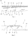
- Fig. 1 shows a preferred embodiment of the optical device 1 for controlling light from an external light source 2 (which is not part of this embodiment), e.g. a laser diode with a Gaussian beam shape.
- the optical device 1 comprises a first waveguide 3, a second waveguide 4 and one further waveguide. It may of course include more than one further waveguides.
- the optical device 1 comprises a first beam shaping structure 5 with a first light emitting area 6 and a second beam shaping structure 7 with a second light emitting area 8.
- the optical device 1 also comprises a bus waveguide 9.
- the bus waveguide 9 is configured for guiding a light beam emitted from the external light source and has a first optical coupler 10 and a second optical coupler 11, wherein the first optical coupler 10 couples a light beam emitted from the external light source from the bus waveguide 9 to the first waveguide 3 and the second optical coupler 11 couples a light beam emitted from the external light source from the bus waveguide 9 to the second waveguide 4. More concretely, each of the optical couplers 10, 11 redirects a fraction of the light beam guided by the bus waveguide 9 to the respective first and second waveguide 3, 4. Subsequently, the first waveguide 3 guides the light beam emitted from the external light source to the first beam shaping structure 5 and the second waveguide 4 guides the light beam emitted from the external light source to the second beam shaping structure 7.
- the first beam shaping structure 5 and the second beam shaping structure 7 are each configured such that the uniformity of the radiant density profile of a light beam emitted from the respective light emitting area 6, 8 of the respective beam shaping structure 5, 7 is higher than that of the light beam guided to the respective beam shaping structure 5, 7 by the respective waveguide 3, 4.
- the first and the second beam shaping structure 5, 7 each comprise a respective optical shaping element 12 and the first and the second waveguides 3, 4 direct the light beam emitted from the external light source at the respective optical shaping element 12.
- the optical shaping elements 12 are configured for manipulating the wavefront of the light beam directed at the respective optical shaping element 12.
- the optical shaping elements 12 are optical diverging element 13, in particular (curved) micro-mirrors, which widen the opening angle of the light beam. Due to the widening of the beam angle, the light emitting areas 6, 8 can also be closer to the respective optical shaping elements 12, while providing the same total area of illumination.
- the optical device 1 comprises a transparent substrate 14.
- the first waveguide 3, the second waveguide 4 and the bus waveguide 9 are formed within the transparent substrate 14, in particular by direct laser writing.
- a front surface of the transparent substrate 14 provides an interface 15, which in the present case is a boundary of the substrate 14 and air.
- the first and the second light emitting areas 6, 8 are provided by the interface 15.
- the first and the second light emitting areas 6, 8 area each delimited by total internal reflection occurring outside the respective light emitting area 6, 8 for the light beam directed towards the interface 15 after interfering with the respective optical shaping element 12. It is noted that in Fig. 1 only that part of the beam reflected from the optical shaping elements 12 is shown which passes the interface 15, i.e. which is not subject to total internal reflection at the interface 15. In contrast, in Fig.
- the optical diverging element 13 By using the optical diverging element 13 to widen the light beam and subsequently the total internal reflection at the interface 15, the uniformity of the radiant density profile of the light beam emitted from the respective light emitting area 6, 8 can be increased.
- the optical shaping elements 12 could of course be optical profiler elements 19 (see Fig. 5 and 6 ), which can increase the uniformity of the radiant density profile of the light beam emitted from the respective light emitting area 6, 8 (in combination with total internal reflection at the interface 15, or without as well).
- the critical angle of total reflection is, as is well known, determined by the refractive indices of the transparent substrate and the - in this embodiment - air.
- the optical shaping elements 12 (or their widening of the light beam, respectively), their distance from the interface 15 and the critical angle of total reflection at the interface 15 (or the relevant refractive indices, respectively) are configured such that the first light emitting area 6 is not overlapping with the second light emitting areas 8.
- the first and the second beam shaping structures 5, 7 are consequently formed by the respective optical shaping element 12 and the interface 15, at which total reflection occurs outside the respective light emitting area 6, 8.
- Fig. 1 is a view of a section parallel to the smaller dimensions of the transparent substrate 14.
- the optical shaping elements 12 are formed at a backside face of the transparent substrate 14.
- the backside face (excluding the indentation forming the optical shaping elements 12) is substantially parallel to the interface 15.
- that part of the light beam that was reflected from the interface 15 due to total internal reflection could either leave the substrate through the backside face (if it has a higher critical angle than the interface), or be repeatedly reflected from the backside face and the front surface of the substrate, such that it will in the end be emitted from the side faces of the substrate 14.
- the optical device 1 further comprises an optical beam divergence reducing structure 16 for reducing the beam divergence of the light beams emitted from the first and the second light emitting area 6, 8.
- the optical beam divergence reducing structure 16 is a DOE which preferably transforms the light emitting from the light emitting areas 6, 8 into (spatially limited) plane waves.
- Fig. 1 shows an SLM 17 for modulating the phase of emitted light on top of the optical device 1. Instead of the SLM 17, also DOEs could be used to create static light pattern.
- Fig. 1 can also be considered to show a detail of an optical system 18, in particular excluding the external light source.
- Fig. 2 to 6 each show a detail of a preferred embodiment of the optical device; 1. For example, they do not show the second waveguide 4.
- the optical device 1 works analogously to the one described in the context of Fig. 1 .
- the light beam emitted from an external light source 2 (not part of the optical device 1) is guided by a bus waveguide 9 and partially coupled to the first waveguide 3, which in turn directs the light beam at the optical shaping element 12, which is an optical diverging element 13.
- the optical shaping element 12 is a micro-mirror formed by a backside face of the substrate 14.
- the optical shaping element 12 is formed as a DOE touching and aligned with the backside face of the substrate 14.
- the optical shaping element 12 in Fig. 5 and 6 may simultaneously be an optical profiler element 19.
- the optical shaping element 12 widens the opening angle of the light beam directed at the optical shaping element 12.
- the embodiments shown in Fig. 3 to 6 further comprise a honeycomb structure 20 with the border of one cell 21 encompassing the first light emitting area 6.
- the honeycomb structure 20 is on top of and touching a light emitting surface 28, which provides the first light emitting area 6.
- the light emitting surface 28 is in this embodiment provided by the front surface of the substrate 14, i.e. (in this embodiment) the interface 15.
- the honeycomb structure 20 is made of an absorptive material.
- the total internal reflection at the interface 15 usually only allows the light emitting areas 6, 8 to be elliptical.
- the light emitting areas 6, 8 can for example be circular in case the optical shaping elements 12 are micro-mirrors, or can be of any shape, in case the optical shaping elements 12 are DOEs.
- the honeycomb structure 20 has a certain (cell) height normal to the front surface of the substrate 14.
- the area illuminated by the individual light emitting areas 6, 8 can be shaped by the walls of the cell 21 having a varying distance from the respective light emitting area 6, 8 (see Fig. 8 ) and therefore absorbing varying fractions of the light beam emitted from border regions of the light emitting areas 6, 8
- the embodiments shown in Fig. 3 to 6 further comprise an optical beam divergence reducing structure 16.
- the light beams will ultimately be emitted from the optical device 1 in Fig. 3 to 6 as a (spatially limited) plane wave, which it is not in Fig. 2 .
- the fat arrows indicate the direction of the light beams and in particular their refraction and reflection at the interface 15. It is noted that those arrows are only for illustration purposes and are not precise; for example, in Fig. 3 to 6 , they already seem to indicate a plane wave prior to the optical beam divergence reducing structure 16, which is not the case.
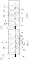
- Fig. 7 and 8 are top views of the backlight unit 22, which includes the optical system 1 and the external light source 2.
- the optical system 1 works similar as described in the context of Fig. 1 to 6 .
- the light beam emitted from the external light source 2 is coupled into the higher ranking bus waveguide 9, from where a fraction is in turn coupled into the lower-ranking bus waveguide 9. Both from the higher ranking and the lower ranking bus waveguides 9, the light beam is coupled into waveguides 3, 4 and guided to the beam shaping structures 5, 7.
- the embodiment of Fig. 8 includes, in contrast to the embodiment of Fig. 7 , a honeycomb structure 20. It can be seen that the cells 21 of the honeycomb structure 20 are hexagonal and each encompass one light emitting area 6, 8, such that the filling factor of illumination of a larger area can be increased.
- Fig. 9 is a diagrammatic sectional view of the embodiment of the backlight unit 22 of Fig. 8 along the plane indicated by A in Fig. 8 (normal to the drawing plane). It can be seen that for this section along line A, the walls of the cells 21 of the honeycomb structure 20 are distanced from the light emitting areas 6, 8.
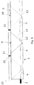
- Fig. 10 shows a Mach-Zehnder-like structure, which can be used to determine temperature dependent changes in optical path lengths and therefore phase changes.
- a light beam is coupled from the external light source 2 into a waveguide in the substrate 14, which waveguide can for example be a bus waveguide 9. From that waveguide, the light beam is coupled into a first interferometer waveguide 23, formed within the substrate 14. A fraction of the light beam is then coupled into the second interferometer waveguide 24 by the first interferometer coupler 25. Subsequently, the light beam is coupled from the second interferometer waveguide 24 back into the first interferometer waveguide 23, where it interferes with that fraction of the light beam, which was not coupled into the second interferometer waveguide 24.
- the interference of the light beam which solely propagated in the first interferometer waveguide 23 and the light beam which also propagated in the second interferometer 24 is measured in the photodetector 27 connected to the first interferometer waveguide 23.
- Thermal expansion of the substrate 14 will then lead to changes in the interference measured by the photodetector 27 (depending, e.g., on the path of the first and the second interferometer waveguides 23, 24).
- Fig. 10 shows a second Mach-Zehnder-like structure, wherein the second interferometer waveguide 24' is connected to the first interferometer waveguide 23' at a shorter distance than for the Mach-Zehnder-like structure formed by the interferometer waveguides 23, 24.
- the light beam of the second Mach-Zehnder-like structure is then coupled into another photodetector 27'.
Landscapes
- Physics & Mathematics (AREA)
- General Physics & Mathematics (AREA)
- Optics & Photonics (AREA)
- Engineering & Computer Science (AREA)
- Microelectronics & Electronic Packaging (AREA)
- Optical Integrated Circuits (AREA)
- Liquid Crystal (AREA)
- Holo Graphy (AREA)
- Diffracting Gratings Or Hologram Optical Elements (AREA)
- Optical Couplings Of Light Guides (AREA)
- Planar Illumination Modules (AREA)
Priority Applications (6)
| Application Number | Priority Date | Filing Date | Title |
|---|---|---|---|
| ES19425085T ES3061332T3 (en) | 2019-12-04 | 2019-12-04 | Optical device for controlling light from an external light source |
| EP19425085.8A EP3832201B1 (de) | 2019-12-04 | 2019-12-04 | Optische vorrichtung zur steuerung von licht aus einer externen lichtquelle |
| KR1020227022939A KR20220110807A (ko) | 2019-12-04 | 2020-12-04 | 외부 광원으로부터의 광을 제어하기 위한 광학 장치 |
| PCT/EP2020/084677 WO2021110936A1 (en) | 2019-12-04 | 2020-12-04 | Optical device for controlling light from an external light source |
| CN202080086762.1A CN114829837B (zh) | 2019-12-04 | 2020-12-04 | 用于控制来自外部光源的光的光学装置 |
| US17/756,734 US12001043B2 (en) | 2019-12-04 | 2020-12-04 | Optical device for controlling light from an external light source |
Applications Claiming Priority (1)
| Application Number | Priority Date | Filing Date | Title |
|---|---|---|---|
| EP19425085.8A EP3832201B1 (de) | 2019-12-04 | 2019-12-04 | Optische vorrichtung zur steuerung von licht aus einer externen lichtquelle |
Publications (3)
| Publication Number | Publication Date |
|---|---|
| EP3832201A1 true EP3832201A1 (de) | 2021-06-09 |
| EP3832201C0 EP3832201C0 (de) | 2026-01-14 |
| EP3832201B1 EP3832201B1 (de) | 2026-01-14 |
Family
ID=69185298
Family Applications (1)
| Application Number | Title | Priority Date | Filing Date |
|---|---|---|---|
| EP19425085.8A Active EP3832201B1 (de) | 2019-12-04 | 2019-12-04 | Optische vorrichtung zur steuerung von licht aus einer externen lichtquelle |
Country Status (6)
| Country | Link |
|---|---|
| US (1) | US12001043B2 (de) |
| EP (1) | EP3832201B1 (de) |
| KR (1) | KR20220110807A (de) |
| CN (1) | CN114829837B (de) |
| ES (1) | ES3061332T3 (de) |
| WO (1) | WO2021110936A1 (de) |
Cited By (2)
| Publication number | Priority date | Publication date | Assignee | Title |
|---|---|---|---|---|
| WO2023002003A1 (en) * | 2021-07-23 | 2023-01-26 | Vitrealab Gmbh | Stereoscopic display device |
| WO2025253331A1 (en) | 2024-06-06 | 2025-12-11 | Politecnico Di Milano | Engineered microscope slide for structured illumination |
Families Citing this family (1)
| Publication number | Priority date | Publication date | Assignee | Title |
|---|---|---|---|---|
| DE102024128814A1 (de) * | 2024-10-07 | 2026-04-09 | Trumpf Photonic Components Gmbh | Anordnung mit einem VCSEL |
Citations (7)
| Publication number | Priority date | Publication date | Assignee | Title |
|---|---|---|---|---|
| WO2007046100A2 (en) * | 2005-10-18 | 2007-04-26 | Oms Displays Ltd. | Device and method for optical resizing and backlighting |
| US20090180282A1 (en) * | 2008-01-15 | 2009-07-16 | Rohm And Haas Denmark Finance A/S | Multilayered integrated backlight illumination assembly |
| US20100259804A1 (en) * | 2007-12-03 | 2010-10-14 | Seereal Technologies S.A. | Illumination Unit Comprising an Optical Wave Guide and an Imaging Means |
| US20110102804A1 (en) * | 2009-11-02 | 2011-05-05 | Cornell University | Passively-thermally-stabilized photonic apparatus, method, and applicatons |
| US20130100696A1 (en) * | 2010-04-23 | 2013-04-25 | Osram Opto Semiconductors Gmbh | Surface Light Source |
| US20130308339A1 (en) | 2012-05-18 | 2013-11-21 | Reald Inc. | Directional backlight |
| US9395690B2 (en) | 2010-07-06 | 2016-07-19 | Seereal Technologies S.A. | Beam divergence and various collimators for holographic or stereoscopic displays |
Family Cites Families (7)
| Publication number | Priority date | Publication date | Assignee | Title |
|---|---|---|---|---|
| JPH06347666A (ja) * | 1993-06-11 | 1994-12-22 | Fuji Photo Film Co Ltd | グレーティングカプラ |
| US5668903A (en) * | 1994-12-22 | 1997-09-16 | Ceramoptec Industries, Inc. | Compound laser system for high power densities |
| KR100444268B1 (ko) * | 2002-06-05 | 2004-08-12 | 주식회사 한택 | 평면배열형 수광 소자를 이용한 광 측정 장치 및 방법 |
| WO2007015402A1 (ja) * | 2005-08-04 | 2007-02-08 | Matsushita Electric Industrial Co., Ltd. | ディスプレイ装置及び照射装置 |
| US8201982B2 (en) * | 2007-12-06 | 2012-06-19 | Panasonic Corporation | Planar illumination device and liquid crystal display device using the same |
| WO2016004511A1 (en) * | 2014-07-11 | 2016-01-14 | National Research Council Of Canada | Forming an optical grating with an apparatus providing an adjustable interference pattern |
| US9851571B1 (en) * | 2016-07-28 | 2017-12-26 | Coherent, Inc. | Apparatus for generating a line-beam from a diode-laser array |
-
2019
- 2019-12-04 EP EP19425085.8A patent/EP3832201B1/de active Active
- 2019-12-04 ES ES19425085T patent/ES3061332T3/es active Active
-
2020
- 2020-12-04 KR KR1020227022939A patent/KR20220110807A/ko active Pending
- 2020-12-04 CN CN202080086762.1A patent/CN114829837B/zh active Active
- 2020-12-04 US US17/756,734 patent/US12001043B2/en active Active
- 2020-12-04 WO PCT/EP2020/084677 patent/WO2021110936A1/en not_active Ceased
Patent Citations (7)
| Publication number | Priority date | Publication date | Assignee | Title |
|---|---|---|---|---|
| WO2007046100A2 (en) * | 2005-10-18 | 2007-04-26 | Oms Displays Ltd. | Device and method for optical resizing and backlighting |
| US20100259804A1 (en) * | 2007-12-03 | 2010-10-14 | Seereal Technologies S.A. | Illumination Unit Comprising an Optical Wave Guide and an Imaging Means |
| US20090180282A1 (en) * | 2008-01-15 | 2009-07-16 | Rohm And Haas Denmark Finance A/S | Multilayered integrated backlight illumination assembly |
| US20110102804A1 (en) * | 2009-11-02 | 2011-05-05 | Cornell University | Passively-thermally-stabilized photonic apparatus, method, and applicatons |
| US20130100696A1 (en) * | 2010-04-23 | 2013-04-25 | Osram Opto Semiconductors Gmbh | Surface Light Source |
| US9395690B2 (en) | 2010-07-06 | 2016-07-19 | Seereal Technologies S.A. | Beam divergence and various collimators for holographic or stereoscopic displays |
| US20130308339A1 (en) | 2012-05-18 | 2013-11-21 | Reald Inc. | Directional backlight |
Cited By (2)
| Publication number | Priority date | Publication date | Assignee | Title |
|---|---|---|---|---|
| WO2023002003A1 (en) * | 2021-07-23 | 2023-01-26 | Vitrealab Gmbh | Stereoscopic display device |
| WO2025253331A1 (en) | 2024-06-06 | 2025-12-11 | Politecnico Di Milano | Engineered microscope slide for structured illumination |
Also Published As
| Publication number | Publication date |
|---|---|
| ES3061332T3 (en) | 2026-04-01 |
| EP3832201C0 (de) | 2026-01-14 |
| US12001043B2 (en) | 2024-06-04 |
| CN114829837A (zh) | 2022-07-29 |
| CN114829837B (zh) | 2025-03-11 |
| WO2021110936A1 (en) | 2021-06-10 |
| EP3832201B1 (de) | 2026-01-14 |
| KR20220110807A (ko) | 2022-08-09 |
| US20230020133A1 (en) | 2023-01-19 |
Similar Documents
| Publication | Publication Date | Title |
|---|---|---|
| US11079541B2 (en) | Optical deflection device and LIDAR apparatus | |
| US20220244360A1 (en) | Hybrid two-dimensional steering lidar | |
| US6829417B2 (en) | Amplitude and phase control in distributed optical structures | |
| US12578586B2 (en) | On-chip mirror beamforming | |
| US12001043B2 (en) | Optical device for controlling light from an external light source | |
| US20230087293A1 (en) | Light Output Devices and Light Outputting Methods for Optical Systems | |
| JP7660126B2 (ja) | 統合制御装置を備えたフェーズドアレイアンテナ付き光電子トランスミッタ | |
| CN115980918B (zh) | 温度不敏感滤波器 | |
| WO2022253149A1 (zh) | 衍射波导、光学组件和电子设备 | |
| CN116507851A (zh) | 具有模间耦合的平板波导和投射器 | |
| KR20220085478A (ko) | 폴리머 광ic 기반 레이저 집적형 이차원 빔스캐너 및 그의 제조 방법 | |
| US20240094466A1 (en) | Light Output Devices and Light Outputting Methods for Optical Systems | |
| JP2005525604A (ja) | 可変光減衰器の方法及びデバイス | |
| WO2020079862A1 (ja) | 光合波器、光源モジュール、2次元光走査装置及び画像投影装置 | |
| CA2910498C (en) | Field inversion waveguide using micro-prism array | |
| CN114791641A (zh) | 一种衍射光学器件及终端设备 | |
| CN108333681B (zh) | 基于部分透射式角反射镜组的片上集成部分反射器 | |
| CN105116488A (zh) | 一种光功率分束器 | |
| WO2024043872A1 (en) | Gratings with reduced diffraction efficiencies beyond fabrication limits | |
| CN217689504U (zh) | 可调光学滤波器 | |
| Xin | Silicon-based Polarization-insensitive Optical Antenna Design and Experimental Characterization of Optical Phased Arrays | |
| Voskerchyan | Integrated RGB Beam Combiner in Al2O3 Photonic Circuits with On-Chip Modulation for AR/VR Displays | |
| WO2025235812A1 (en) | Systems and methods for integrated free space optical elements and devices | |
| JP2015059978A (ja) | 波長選択スイッチ | |
| CN118409390A (zh) | 光波导及显示设备 |
Legal Events
| Date | Code | Title | Description |
|---|---|---|---|
| PUAI | Public reference made under article 153(3) epc to a published international application that has entered the european phase |
Free format text: ORIGINAL CODE: 0009012 |
|
| STAA | Information on the status of an ep patent application or granted ep patent |
Free format text: STATUS: THE APPLICATION HAS BEEN PUBLISHED |
|
| AK | Designated contracting states |
Kind code of ref document: A1 Designated state(s): AL AT BE BG CH CY CZ DE DK EE ES FI FR GB GR HR HU IE IS IT LI LT LU LV MC MK MT NL NO PL PT RO RS SE SI SK SM TR |
|
| STAA | Information on the status of an ep patent application or granted ep patent |
Free format text: STATUS: REQUEST FOR EXAMINATION WAS MADE |
|
| 17P | Request for examination filed |
Effective date: 20211207 |
|
| RBV | Designated contracting states (corrected) |
Designated state(s): AL AT BE BG CH CY CZ DE DK EE ES FI FR GB GR HR HU IE IS IT LI LT LU LV MC MK MT NL NO PL PT RO RS SE SI SK SM TR |
|
| STAA | Information on the status of an ep patent application or granted ep patent |
Free format text: STATUS: EXAMINATION IS IN PROGRESS |
|
| 17Q | First examination report despatched |
Effective date: 20220902 |
|
| RAP3 | Party data changed (applicant data changed or rights of an application transferred) |
Owner name: CONSIGLIO NAZIONALE DELLE RICERCHE Owner name: VITREALAB GMBH |
|
| RIN1 | Information on inventor provided before grant (corrected) |
Inventor name: OSELLAME, ROBERTO Inventor name: GREGANTI, CHIARA Inventor name: ZEUNER, JONAS |
|
| GRAP | Despatch of communication of intention to grant a patent |
Free format text: ORIGINAL CODE: EPIDOSNIGR1 |
|
| STAA | Information on the status of an ep patent application or granted ep patent |
Free format text: STATUS: GRANT OF PATENT IS INTENDED |
|
| INTG | Intention to grant announced |
Effective date: 20250804 |
|
| GRAS | Grant fee paid |
Free format text: ORIGINAL CODE: EPIDOSNIGR3 |
|
| GRAA | (expected) grant |
Free format text: ORIGINAL CODE: 0009210 |
|
| STAA | Information on the status of an ep patent application or granted ep patent |
Free format text: STATUS: THE PATENT HAS BEEN GRANTED |
|
| AK | Designated contracting states |
Kind code of ref document: B1 Designated state(s): AL AT BE BG CH CY CZ DE DK EE ES FI FR GB GR HR HU IE IS IT LI LT LU LV MC MK MT NL NO PL PT RO RS SE SI SK SM TR |
|
| REG | Reference to a national code |
Ref country code: CH Ref legal event code: F10 Free format text: ST27 STATUS EVENT CODE: U-0-0-F10-F00 (AS PROVIDED BY THE NATIONAL OFFICE) Effective date: 20260114 Ref country code: GB Ref legal event code: FG4D |
|
| REG | Reference to a national code |
Ref country code: DE Ref legal event code: R096 Ref document number: 602019080307 Country of ref document: DE |
|
| REG | Reference to a national code |
Ref country code: IE Ref legal event code: FG4D |
|
| U01 | Request for unitary effect filed |
Effective date: 20260120 |
|
| U07 | Unitary effect registered |
Designated state(s): AT BE BG DE DK EE FI FR IT LT LU LV MT NL PT RO SE SI Effective date: 20260126 |
|
| REG | Reference to a national code |
Ref country code: ES Ref legal event code: FG2A Ref document number: 3061332 Country of ref document: ES Kind code of ref document: T3 Effective date: 20260401 |