EP3832253A1 - Lichtquellenvorrichtung, bildsensor und sensormodul - Google Patents
Lichtquellenvorrichtung, bildsensor und sensormodul Download PDFInfo
- Publication number
- EP3832253A1 EP3832253A1 EP19844024.0A EP19844024A EP3832253A1 EP 3832253 A1 EP3832253 A1 EP 3832253A1 EP 19844024 A EP19844024 A EP 19844024A EP 3832253 A1 EP3832253 A1 EP 3832253A1
- Authority
- EP
- European Patent Office
- Prior art keywords
- light
- light emitting
- emitting elements
- light emission
- period
- Prior art date
- Legal status (The legal status is an assumption and is not a legal conclusion. Google has not performed a legal analysis and makes no representation as to the accuracy of the status listed.)
- Granted
Links
Images













Classifications
-
- H—ELECTRICITY
- H01—ELECTRIC ELEMENTS
- H01S—DEVICES USING THE PROCESS OF LIGHT AMPLIFICATION BY STIMULATED EMISSION OF RADIATION [LASER] TO AMPLIFY OR GENERATE LIGHT; DEVICES USING STIMULATED EMISSION OF ELECTROMAGNETIC RADIATION IN WAVE RANGES OTHER THAN OPTICAL
- H01S5/00—Semiconductor lasers
- H01S5/40—Arrangement of two or more semiconductor lasers, not provided for in groups H01S5/02 - H01S5/30
- H01S5/42—Arrays of surface emitting lasers
- H01S5/423—Arrays of surface emitting lasers having a vertical cavity
-
- H—ELECTRICITY
- H04—ELECTRIC COMMUNICATION TECHNIQUE
- H04N—PICTORIAL COMMUNICATION, e.g. TELEVISION
- H04N25/00—Circuitry of solid-state image sensors [SSIS]; Control thereof
- H04N25/70—SSIS architectures; Circuits associated therewith
- H04N25/709—Circuitry for control of the power supply
-
- G—PHYSICS
- G01—MEASURING; TESTING
- G01B—MEASURING LENGTH, THICKNESS OR SIMILAR LINEAR DIMENSIONS; MEASURING ANGLES; MEASURING AREAS; MEASURING IRREGULARITIES OF SURFACES OR CONTOURS
- G01B11/00—Measuring arrangements characterised by the use of optical techniques
- G01B11/24—Measuring arrangements characterised by the use of optical techniques for measuring contours or curvatures
- G01B11/25—Measuring arrangements characterised by the use of optical techniques for measuring contours or curvatures by projecting a pattern, e.g. one or more lines, moiré fringes on the object
- G01B11/2513—Measuring arrangements characterised by the use of optical techniques for measuring contours or curvatures by projecting a pattern, e.g. one or more lines, moiré fringes on the object with several lines being projected in more than one direction, e.g. grids, patterns
-
- G—PHYSICS
- G01—MEASURING; TESTING
- G01B—MEASURING LENGTH, THICKNESS OR SIMILAR LINEAR DIMENSIONS; MEASURING ANGLES; MEASURING AREAS; MEASURING IRREGULARITIES OF SURFACES OR CONTOURS
- G01B5/00—Measuring arrangements characterised by the use of mechanical techniques
- G01B5/0011—Arrangements for eliminating or compensation of measuring errors due to temperature or weight
- G01B5/0014—Arrangements for eliminating or compensation of measuring errors due to temperature or weight due to temperature
-
- G—PHYSICS
- G01—MEASURING; TESTING
- G01S—RADIO DIRECTION-FINDING; RADIO NAVIGATION; DETERMINING DISTANCE OR VELOCITY BY USE OF RADIO WAVES; LOCATING OR PRESENCE-DETECTING BY USE OF THE REFLECTION OR RERADIATION OF RADIO WAVES; ANALOGOUS ARRANGEMENTS USING OTHER WAVES
- G01S17/00—Systems using the reflection or reradiation of electromagnetic waves other than radio waves, e.g. lidar systems
- G01S17/88—Lidar systems specially adapted for specific applications
- G01S17/89—Lidar systems specially adapted for specific applications for mapping or imaging
- G01S17/894—Three-dimensional [3D] imaging with simultaneous measurement of time-of-flight at a two-dimensional [2D] array of receiver pixels, e.g. time-of-flight cameras or flash lidar
-
- G—PHYSICS
- G01—MEASURING; TESTING
- G01S—RADIO DIRECTION-FINDING; RADIO NAVIGATION; DETERMINING DISTANCE OR VELOCITY BY USE OF RADIO WAVES; LOCATING OR PRESENCE-DETECTING BY USE OF THE REFLECTION OR RERADIATION OF RADIO WAVES; ANALOGOUS ARRANGEMENTS USING OTHER WAVES
- G01S7/00—Details of systems according to groups G01S13/00, G01S15/00, G01S17/00
- G01S7/48—Details of systems according to groups G01S13/00, G01S15/00, G01S17/00 of systems according to group G01S17/00
- G01S7/497—Means for monitoring or calibrating
-
- H—ELECTRICITY
- H01—ELECTRIC ELEMENTS
- H01S—DEVICES USING THE PROCESS OF LIGHT AMPLIFICATION BY STIMULATED EMISSION OF RADIATION [LASER] TO AMPLIFY OR GENERATE LIGHT; DEVICES USING STIMULATED EMISSION OF ELECTROMAGNETIC RADIATION IN WAVE RANGES OTHER THAN OPTICAL
- H01S5/00—Semiconductor lasers
- H01S5/02—Structural details or components not essential to laser action
- H01S5/024—Arrangements for thermal management
-
- H—ELECTRICITY
- H01—ELECTRIC ELEMENTS
- H01S—DEVICES USING THE PROCESS OF LIGHT AMPLIFICATION BY STIMULATED EMISSION OF RADIATION [LASER] TO AMPLIFY OR GENERATE LIGHT; DEVICES USING STIMULATED EMISSION OF ELECTROMAGNETIC RADIATION IN WAVE RANGES OTHER THAN OPTICAL
- H01S5/00—Semiconductor lasers
- H01S5/04—Processes or apparatus for excitation, e.g. pumping, e.g. by electron beams
- H01S5/042—Electrical excitation ; Circuits therefor
- H01S5/0428—Electrical excitation ; Circuits therefor for applying pulses to the laser
-
- H—ELECTRICITY
- H01—ELECTRIC ELEMENTS
- H01S—DEVICES USING THE PROCESS OF LIGHT AMPLIFICATION BY STIMULATED EMISSION OF RADIATION [LASER] TO AMPLIFY OR GENERATE LIGHT; DEVICES USING STIMULATED EMISSION OF ELECTROMAGNETIC RADIATION IN WAVE RANGES OTHER THAN OPTICAL
- H01S5/00—Semiconductor lasers
- H01S5/02—Structural details or components not essential to laser action
- H01S5/022—Mountings; Housings
- H01S5/0233—Mounting configuration of laser chips
- H01S5/0234—Up-side down mountings, e.g. Flip-chip, epi-side down mountings or junction down mountings
-
- H—ELECTRICITY
- H01—ELECTRIC ELEMENTS
- H01S—DEVICES USING THE PROCESS OF LIGHT AMPLIFICATION BY STIMULATED EMISSION OF RADIATION [LASER] TO AMPLIFY OR GENERATE LIGHT; DEVICES USING STIMULATED EMISSION OF ELECTROMAGNETIC RADIATION IN WAVE RANGES OTHER THAN OPTICAL
- H01S5/00—Semiconductor lasers
- H01S5/06—Arrangements for controlling the laser output parameters, e.g. by operating on the active medium
- H01S5/062—Arrangements for controlling the laser output parameters, e.g. by operating on the active medium by varying the potential of the electrodes
- H01S5/06209—Arrangements for controlling the laser output parameters, e.g. by operating on the active medium by varying the potential of the electrodes in single-section lasers
- H01S5/06216—Pulse modulation or generation
-
- H—ELECTRICITY
- H01—ELECTRIC ELEMENTS
- H01S—DEVICES USING THE PROCESS OF LIGHT AMPLIFICATION BY STIMULATED EMISSION OF RADIATION [LASER] TO AMPLIFY OR GENERATE LIGHT; DEVICES USING STIMULATED EMISSION OF ELECTROMAGNETIC RADIATION IN WAVE RANGES OTHER THAN OPTICAL
- H01S5/00—Semiconductor lasers
- H01S5/10—Construction or shape of the optical resonator, e.g. extended or external cavity, coupled cavities, bent-guide, varying width, thickness or composition of the active region
- H01S5/18—Surface-emitting [SE] lasers, e.g. having both horizontal and vertical cavities
- H01S5/183—Surface-emitting [SE] lasers, e.g. having both horizontal and vertical cavities having only vertical cavities, e.g. vertical cavity surface-emitting lasers [VCSEL]
- H01S5/18305—Surface-emitting [SE] lasers, e.g. having both horizontal and vertical cavities having only vertical cavities, e.g. vertical cavity surface-emitting lasers [VCSEL] with emission through the substrate, i.e. bottom emission
-
- H—ELECTRICITY
- H04—ELECTRIC COMMUNICATION TECHNIQUE
- H04N—PICTORIAL COMMUNICATION, e.g. TELEVISION
- H04N25/00—Circuitry of solid-state image sensors [SSIS]; Control thereof
- H04N25/70—SSIS architectures; Circuits associated therewith
- H04N25/76—Addressed sensors, e.g. MOS or CMOS sensors
- H04N25/77—Pixel circuitry, e.g. memories, A/D converters, pixel amplifiers, shared circuits or shared components
- H04N25/771—Pixel circuitry, e.g. memories, A/D converters, pixel amplifiers, shared circuits or shared components comprising storage means other than floating diffusion
Definitions
- the present technology relates to light source devices, image sensors, and sensing modules, and particularly relates to a technical field of capturing reflected light of light emitted from a light source device with an image capturing device and sensing a distance, shape, and the like.
- a technology of a distance measuring device that estimates a distance to an object and a three-dimensional (3D) shape of the object by emitting light from a light source device serving as a multi-lamp laser in which a plurality of laser light emitting elements is disposed and capturing reflected light from the detected object with an image capturing device including an image sensor.
- Patent Document 1 discloses a method of calculating a distance from a plurality of pieces of image obtained by accumulating a plurality of light emissions with a constant cycle and pulse width as a distance measuring system using time of flight.
- Patent Document 1 Japanese Patent Application Laid-Open No. 2017-517737
- control is performed such that light emission time on the light source device side and exposure time on the image sensor side agree with each other.
- the upper limit of the exposure time is determined by the heat generated on the light source side.
- sensing precision may decrease because sufficient exposure cannot be performed, accurate coordinates cannot be detected from captured data, and the like.
- a purpose of the present technology is to make it possible to inhibit the temperature rise of the light source while implementing desired exposure time.
- a light source device includes: a plurality of laser light emitting elements; and a drive unit configured to drive each of the laser light emitting elements to perform a plurality of light emissions in one frame period in an image sensor that receives and captures light emitted from the plurality of laser light emitting elements and reflected by a subject.
- distance measurement, object recognition, and the like are performed by causing the light emitted from the plurality of laser light emitting elements of the light source device to be reflected by the subject and receiving and capturing the reflected light by the image sensor.
- the laser emits light continuously, temperature rise increases.
- the drive unit changes the number of light emissions of the laser light emitting elements in one frame period according to a temperature detection result.
- one light emission is performed in one frame period, and if the temperature rise is detected, a plurality of light emissions is performed in one frame period.
- the drive unit changes the number of light emissions of the laser light emitting elements as a plurality of light emissions in one frame period according to a temperature detection result.
- the number of emissions as the plurality of light emissions is switched, such as two light emissions or three light emissions in one frame period.
- the laser light emitting elements include vertical cavity surface emitting lasers.
- the light source device called a vertical cavity surface emitting laser (VCSEL) is assumed.
- the light source device further includes a temperature sensor configured to detect a temperature near the laser light emitting elements.
- the temperature sensor is disposed near the laser light emitting elements as VCSEL.
- a temperature sensor configured to detect a temperature near the laser light emitting elements is further provided, and the drive unit performs light emission suspension and light emission resumption of the laser light emitting elements in one frame period according to a detection result of the temperature sensor.
- the drive unit drives each of the laser light emitting elements according to a light emission parameter that defines a light emission operation of the laser light emitting elements per predetermined unit.
- the predetermined unit is a unit of one laser light emitting element, a unit of a blocked plurality of laser light emitting elements, and the like.
- the drive unit has a configuration to perform a different light emission operation for each predetermined unit.
- the drive unit drives each of the laser light emitting elements according to a light emission parameter that defines a light emission operation of the laser light emitting elements
- the light source device includes a control unit configured to generate the light emission parameter
- the control unit is provided to generate the light emission parameter that sets the number of light emissions of the laser light emitting elements in one frame period according to temperature conditions.
- the drive unit controls duration time of one light emission of the plurality of light emissions with a set light emission parameter.
- the light emission period length of each of the plurality of light emissions is set with the light emission parameter.
- the drive unit controls a light emission interval of the plurality of light emissions with a set light emission parameter.
- the light emission interval (non-light emission period) in a case where each of the plurality of light emissions is performed is set with the light emission parameter.
- An image sensor includes a photoelectric conversion unit configured, in a case where a plurality of laser light emitting elements of a light source device performs a plurality of light emissions in one frame period in which a captured image is generated, to perform exposure to light emitted from the laser light emitting elements and reflected by a subject in an exposure period corresponding to a period of each of the plurality of light emissions, and the image sensor outputs one-frame captured data obtained by a plurality of exposures.
- the light emitted from the light source device is reflected by the subject, and the reflected light is received and captured by the image sensor to perform distance measurement and object recognition.
- a plurality of light emissions is performed in one frame period of the image capturing device.
- the image capturing device (image sensor) performs a plurality of exposures to generate one-frame captured data.
- a charge holding unit is further provided to hold a charge by the exposure of the photoelectric conversion unit according to the period of each of the plurality of light emissions of the laser light emitting elements in one frame period, and a charge signal that generates one image in each frame period is read from the charge holding unit.
- the charge holding unit generates the one-frame charge signal corresponding to a plurality of exposures.
- the photoelectric conversion unit allows settings of an operation of performing exposure corresponding to a period of each of the plurality of light emissions in one frame, and an operation of performing exposure corresponding to a period of a part of the plurality of light emissions.
- the operation of performing exposure corresponding to a period of each of the plurality of light emissions of the laser light emitting elements and the operation of performing exposure in a period of a part of the plurality of light emissions can be selectively performed.
- a sensing module includes: a plurality of laser light emitting elements; a drive unit configured to drive each of the laser light emitting elements to perform a plurality of light emissions in one frame period in an image sensor that receives and captures light emitted from the plurality of laser light emitting elements and reflected by a subject; and the image sensor including a photoelectric conversion unit configured to perform exposure to the light emitted from the laser light emitting elements and reflected by the subject in an exposure period corresponding to a period of each of the plurality of light emissions, the image sensor outputting one-frame captured data obtained by a plurality of the exposures.
- the sensing module that performs distance measurement and object recognition is configured.
- This sensing module is a distance measuring system that estimates a 3D shape of an object by causing light emitted from a light source to be reflected by an object, capturing the reflected light with the image sensor, and performing signal processing on the basis of a capturing result.
- the sensing module performs a plurality of light emissions from the light source in order to obtain one-time captured image, and estimates the distance, 3D shape of the object, and the like by using one piece of captured image generated by accumulating the reflected light of the plurality of light emissions.
- a temperature sensor configured to detect a temperature near the laser light emitting elements is further provided.
- the drive unit changes the number of light emissions of the laser light emitting elements in one frame period according to a temperature detection result by the temperature sensor.
- one light emission is performed in one frame period, and if the temperature rise is detected, a plurality of light emissions is performed in one frame period.
- the present technology by dividing the light emission into a plurality of light emissions, it is possible to inhibit the temperature rise of the light source while implementing desired exposure time, and as a result, it is possible to contribute to improvement in light emission efficiency.
- Fig. 1 shows a configuration example of a distance measuring device 1 as embodiments according to the present technology.
- the distance measuring device 1 has a configuration including a light source device 100 and an image capturing device 101.
- the distance measuring device 1 includes: a light emitting unit 2, a drive unit 3, a power circuit 4, a light emission side optical system 5, and a temperature detecting unit 10 as the light source device 100; and an image capturing side optical system 6, an image sensor 7, and an image processing unit 8 as the image capturing device 101. Furthermore, the distance measuring device 1 includes a control unit 9.
- the control unit 9 may be included in the light source device 100, may be included in the image capturing device 101, or may be configured separately from the light source device 100 or the image capturing device 101.
- the light emitting unit 2 emits light from a plurality of light sources.
- the light emitting unit 2 of this example includes laser light emitting elements 2a by VCSEL as each light source (hereinafter, also simply referred to as "light emitting elements 2a").
- the light emitting elements 2a are arranged, for example, in a predetermined manner such as a matrix.
- the drive unit 3 includes an electric circuit for driving the light emitting unit 2.
- the power circuit 4 generates a power voltage for the drive unit 3 (drive voltage Vd as described later), for example, on the basis of an input voltage from a battery and the like (not shown) provided in the distance measuring device 1 (input voltage Vin as described later).
- the drive unit 3 drives the light emitting unit 2 on the basis of the power voltage.
- the light emitted from the light emitting unit 2 is emitted to a subject S as a distance measuring target via the light emission side optical system 5. Then, the reflected light of the thus emitted light from the subject S enters an image capturing surface of the image sensor 7 via the image capturing side optical system 6.
- the image sensor 7 is, for example, an image capturing element such as a charge coupled device (CCD) sensor or a complementary metal oxide semiconductor (CMOS) sensor, and receives the reflected light that enters from the subject S via the image capturing side optical system 6 as described above, converts the reflected light into an electric signal and outputs the electric signal.
- CCD charge coupled device
- CMOS complementary metal oxide semiconductor
- the image sensor 7 performs, for example, correlated double sampling (CDS) processing, automatic gain control (AGC) processing, and the like on the electric signal obtained by photoelectrically converting the received light, and further performs analog/digital (A/D) conversion processing. Then, the image sensor 7 outputs an image signal as digital data to the image processing unit 8 in the subsequent stage.
- CDS correlated double sampling
- AGC automatic gain control
- A/D analog/digital
- the image sensor 7 of this example outputs a frame synchronization signal Fs to the drive unit 3. This allows the drive unit 3 to cause the light emitting elements 2a in the light emitting unit 2 to emit light at timing according to a frame cycle of the image sensor 7.
- the image processing unit 8 is configured as an image processing processor by, for example, a digital signal processor (DSP) and the like.
- DSP digital signal processor
- the image processing unit 8 performs various types of image signal processing on a digital signal (image signal) input from the image sensor 7.
- the control unit 9 includes, for example, a microcomputer having a central processing unit (CPU), a read only memory (ROM), a random access memory (RAM), and the like or an information processing device such as a DSP.
- the control unit 9 controls the drive unit 3 for controlling a light emission operation by the light emitting unit 2, and controls the image capturing operation by the image sensor 7.
- the control unit 9 has a function as a distance measuring unit 9a.
- the distance measuring unit 9a measures a distance to the subject S on the basis of the image signal input via the image processing unit 8 (that is, image signal obtained by receiving the reflected light from the subject S).
- the distance measuring unit 9a of this example measures the distance to each part of the subject S in order to enable identification of a three-dimensional shape of the subject S.
- control unit 9 may be configured to control the power circuit 4.
- the temperature detecting unit 10 detects a temperature of the light emitting unit 2.
- the temperature detecting unit 10 can have a configuration to detect the temperature by using, for example, a diode.
- a detection signal by the temperature detecting unit 10 is detected by the control unit 53 and necessary control is performed.
- the drive unit 3 detects the detection signal by the temperature detecting unit 10 and the drive unit 3 changes the drive of the light emitting elements 2a of the light emitting unit 2.
- distance measurement methods using the structured light (STL) technique or time of flight (ToF) technique can be adopted.
- the STL technique is, for example, a technique for measuring a distance on the basis of an image obtained by capturing an image of the subject S on which light having a predetermined light/dark pattern such as a dot pattern or a grid pattern is emitted.
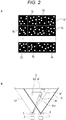
- Fig. 2 is an explanatory diagram of the STL technique.
- pattern light Lp having a dot pattern as shown in Fig. 2A is emitted on the subject S.
- the pattern light Lp is divided into a plurality of blocks BL, and different dot patterns are assigned to respective blocks BL (dot patterns are not duplicated between blocks B).
- Fig. 2B is an explanatory diagram of the distance measurement principle of the STL technique.
- a wall W and a box BX disposed in front of the wall W are the subject S, and the pattern light Lp is emitted to the subject S.
- BLn in the figure means light of a certain block BL in the pattern light Lp
- dn means the dot pattern of the block BLn that appears on the image captured by the image sensor 7.
- the dot pattern of the block BLn appears at the position of "dn'" in the figure in the captured image. That is, the position where the pattern of the block BLn appears in the captured image differs between in a case where the box BX exists and in a case where the box BX does not exist. Specifically, pattern distortion occurs.
- the STL technique is a technique to obtain the shape and depth of the subject S by using the fact that the pattern emitted in this way is distorted by the object shape of the subject S. Specifically, this is a technique to obtain the shape and depth of the subject S from the distortion of the pattern.
- the distance measuring unit 9a controls the drive unit 3 such that the light emitting unit 2 emits the pattern light, and detects the pattern distortion in the image signal obtained via the image processing unit 8 and calculates the distance on the basis of how the pattern is distorted.
- IR infrared
- the ToF technique is a technique to measure the distance to the object by detecting the time of flight (time difference) of the light emitted from the light emitting unit 2 until the light is reflected by the object and reaches the image sensor 7.
- the distance measuring unit 9a calculates the time difference from light emission to light reception of the light emitted from the light emitting unit 2 and received by the image sensor 7, and calculates the distance to each part of the subject S on the basis of the time difference and the speed of light.
- an IR image sensor is used as the image sensor 7.
- Fig. 3 shows a circuit configuration example of the light source device 100 including the light emitting unit 2, the drive unit 3, and the power circuit 4 shown in Fig. 1 .
- Fig. 3 shows the image sensor 7 and the control unit 9 shown in Fig. 1 together with the circuit configuration example of the light source device 100.
- the light emitting unit 2, the drive unit 3, and the power circuit 4 are formed on a common substrate (substrate B as described later).
- a configuration unit including at least the light emitting unit 2 and formed on a substrate common to the light emitting unit 2 is referred to as the light source device 100.
- the light source device 100 includes the temperature detecting unit 10 together with the light emitting unit 2, the drive unit 3, and the power circuit 4.
- the light emitting unit 2 includes the plurality of light emitting elements 2a as VCSEL as described above.
- the number of light emitting elements 2a is set at "4" for convenience of illustration, but the number of light emitting elements 2a in the light emitting unit 2 is not limited to 4, and is only required to be at least 2 or more.
- the power circuit 4 includes a DC/DC converter 40, and generates a drive voltage Vd (DC voltage) to be used by the drive unit 3 to drive the light emitting unit 2 on the basis of the input voltage Vin of a DC voltage.
- Vd DC voltage
- the drive unit 3 includes a drive circuit 30 and a drive control unit 31.
- the drive circuit 30 includes a switching element Q1 and a switch SW for each light emitting element 2a, and also includes a switching element Q2 and a constant current source 30a.
- Field-effect transistors FETs
- MOS metal-oxide-semiconductor
- Each switching element Q1 is connected in parallel to an output line of the DC/DC converter 40, that is, to a supply line of the drive voltage Vd.
- the switching element Q2 is connected in parallel to the switching elements Q1.
- sources of each switching element Q1 and the switching element Q2 are connected to the output line of the DC/DC converter 40.
- a drain of each switching element Q1 is connected to an anode of one corresponding light emitting element 2a of the light emitting elements 2a in the light emitting unit 2.
- each light emitting element 2a is connected to the ground (GND).
- a drain of the switching element Q2 is connected to the ground via the constant current source 30a, and a gate is connected to a connection point of the drain and the constant current source 30a.
- a gate of each switching element Q1 is connected to a gate of the switching element Q2 via one corresponding switch SW.
- the switching element Q1 with the switch SW turned on conducts.
- the drive voltage Vd is applied to the light emitting element 2a connected to the conductive switching element Q1, and the light emitting element 2a emits light.
- a drive current Id flows through the light emitting element 2a.
- the switching element Q1 and the switching element Q2 form a current mirror circuit.
- a current value of the drive current Id is set at a value corresponding to a current value of the constant current source 30a.
- the drive control unit 31 controls ON/OFF of the light emitting elements 2a by controlling ON/OFF of the switches SW in the drive circuit 30.
- the drive control unit 31 determines ON/OFF control timing of the light emitting elements 2a, laser power (current value of the drive current Id), and the like on the basis of an instruction from the control unit 9. For example, the drive control unit 31 receives a value designating these as a light emission parameter from the control unit 9, and controls the drive of the light emitting elements 2a accordingly.
- the frame synchronization signal Fs is supplied from the image sensor 7 to the drive control unit 31, thereby making it possible for the drive control unit 31 to synchronize ON timing and OFF timing of the light emitting elements 2a with a frame cycle of the image sensor 7.
- the drive control unit 31 may have a configuration to transmit the frame synchronization signal Fs and a signal indicating exposure timing to the image sensor 7.
- the control unit 9 may have a configuration to transmit a signal indicating timing of frame synchronization signal Fs emission and exposure to the drive control unit 31 and the image sensor 7.
- Fig. 3 illustrates a configuration in which the switching elements Q1 are provided on the anode side of the light emitting elements 2a, but as in a drive circuit 30A shown in Fig. 4 , it is possible to have a configuration in which the switching elements Q1 are provided on the cathode side of the light emitting elements 2a.
- each light emitting element 2a in the light emitting unit 2 is connected to the output line of the DC/DC converter 40.
- An N-channel MOSFET is used for the switching element Q1 and the switching element Q2 that constitute the current mirror circuit.
- the drain and gate of the switching element Q2 are connected to the output line of the DC/DC converter 40 via the constant current source 30a, and the source is connected to the ground via the constant current source 30a.
- each switching element Q1 is connected to the cathode of the corresponding light emitting element 2a, and the source is connected to the ground.
- the gate of each switching element Q1 is connected to the gate and drain of the switching element Q2 via the corresponding switch SW.
- the drive control unit 31 can turn ON/OFF the light emitting element 2a by controlling the ON/OFF of the switch SW.
- Fig. 5 shows a configuration example of a light source device 100A as a modified example.
- the light source device 100A is provided with a power circuit 4A in place of the power circuit 4, and is provided with a drive unit 3A in place of the drive unit 3.
- the power circuit 4A includes a plurality of the DC/DC converters 40 (two in the example of the figure). An input voltage Vin1 is supplied to one DC/DC converter 40, and an input voltage Vin2 is supplied to the other DC/DC converter 40.
- the drive unit 3A includes a plurality of drive circuits 30 each inputting the drive voltage Vd from the different DC/DC converter 40. As shown in the figure, each drive circuit 30 is provided with a variable current source 30b in place of the constant current source 30a.
- the variable current source 30b is a current source having a variable current value.
- the light emitting elements 2a in the light emitting unit 2 are divided into a plurality of light emitting element groups that undergo ON/OFF control by the different drive circuits 30.
- the drive control unit 31 controls ON/OFF of the switches SW in each drive circuit 30.
- the drive current Id of the light emitting elements 2a at different values for each system. For example, by making the voltage value of the drive voltage Vd and the current value of the variable current source 30b different for each system, it is possible to make the value of the drive current Id different for each system. Furthermore, if the DC/DC converter 40 has a configuration to perform constant current control on the drive current Id, by making target values for the constant current control different between the DC/DC converters 40, it is also possible to make the value of the drive current Id different for each system.
- the light source device 100 can have configurations shown in Figs. 6 to 8 .
- the light source device 100 can have the configuration shown in Fig. 6A in which a chip Ch2 in which a circuit as the light emitting unit 2 is formed, a chip Ch3 in which a circuit as the drive unit 3 is formed, and a chip Ch4 in which the power circuit 4 is formed are formed on the same substrate B.
- the drive unit 3 and the power circuit 4 can be formed on the same chip Ch34, and in this case, the light source device 100 can have a configuration in which the chip Ch2 and the chip Ch34 are formed on the same substrate B as shown in Fig. 6B .
- the light source device 100 can have a configuration in which another chip Ch is mounted on a chip Ch.
- the light source device 100 can have, for example, the configuration as in Fig. 7A in which the chip Ch3 on which the chip Ch2 is mounted and the chip Ch4 are formed on the substrate B, the configuration as in Fig. 7B in which the chip Ch3 on which the chip Ch2 and the chip Ch4 are mounted is formed on the substrate B, or the configuration as in Fig. 7C in which the chip Ch34 on which the chip Ch2 is mounted is formed on the substrate B.
- the light source device 100 can include the image sensor 7.
- Fig. 8A illustrates a configuration of the light source device 100 in which, along with the chip Ch2, the chip Ch3, and the chip Ch4, a chip Ch7 in which a circuit as the image sensor 7 is formed is formed on the same substrate B.
- Fig. 8B illustrates a configuration of the light source device 100 in which the chip Ch34 on which the chip Ch2 is mounted and the chip Ch7 are formed on the same substrate B.
- the light source device 100A described above can also adopt a configuration similar to the configuration described in Figs. 6 to 8 .
- a temperature detecting element such as a diode is only required to be formed at a position near the chip Ch2 on the substrate B (for example, lateral position of the chip Ch2 on the substrate B, and the like).
- the temperature detecting element is only required to be formed at a position near the chip Ch2 on the other chip Ch (for example, position directly below the chip Ch2, and the like).
- the temperature detecting unit 10 may include a plurality of temperature sensors 10a each having a temperature detecting element such as a diode.
- Fig. 9 shows an arrangement example of each temperature sensor 10a in a case where the temperature detecting unit 10 includes the plurality of temperature sensors 10a.
- the plurality of temperature sensors 10a is not positioned exclusively in one place, but is arranged discretely in a plane parallel to a plane on which the light emitting elements 2a are arranged.
- respective temperature sensors 10a can also be arranged at equal intervals in the plane parallel to the plane on which the light emitting elements 2a are arranged.
- Fig. 9 shows an example in which four temperature sensors 10a are arranged for nine light emitting elements 2a, but the number of arranged light emitting elements 2a and temperature sensors 10a is not limited to this example.
- the plurality of temperature sensors 10a By arranging the plurality of temperature sensors 10a discretely as in the example of Fig. 9 , it is possible to detect in-plane temperature distribution of the light emitting unit 2. Furthermore, it is possible to detect and classify the temperature of each area on a light emitting surface, and moreover, it is also possible to detect and classify the temperature of each light emitting element 2a by increasing the number of arranged temperature sensors 10a.
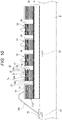
- Fig. 10 shows the structure example of the chip Ch2 in a case where the chip Ch2 is formed on the substrate B as in Figs. 6A, 6B , and 8A .
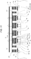
- Fig. 11 shows the structure example of the chip Ch2 in a case where the chip Ch2 is mounted on another chip Ch as in Figs. 7A to 7C and 8B .
- Figs. 10 and 11 show, as one example, the structure example corresponding to the case where the drive circuit 30 is inserted into the anode side of the light emitting element 2a (see Fig. 3 ).
- a part corresponding to each light emitting element 2a is formed as a mesa M.
- a semiconductor substrate 20 is used as the substrate of the chip Ch2.
- a cathode electrode Tc is formed on a lower layer side of the semiconductor substrate 20.
- a gallium arsenide (GaAs) substrate is used for the semiconductor substrate 20.
- a first multilayer film reflector layer 21, an active layer 22, a second multilayer film reflector layer 25, a contact layer 26, and an anode electrode Ta are formed in the order from the lower layer side to the upper layer side in each mesa M.
- a current constriction layer 24 is formed in a part (specifically, lower end) of the second multilayer film reflector layer 25. Furthermore, a part including the active layer 22 and sandwiched between the first multilayer film reflector layer 21 and the second multilayer film reflector layer 25 is a resonator 23.
- the first multilayer film reflector layer 21 includes a compound semiconductor exhibiting N-type conductivity
- the second multilayer film reflector layer 25 includes a compound semiconductor exhibiting P-type conductivity.
- the active layer 22 is a layer for generating laser light
- the current constriction layer 24 is a layer that efficiently injects an electric current into the active layer 22 to bring about a lens effect.
- the current constriction layer 24 includes an oxidized region in the central portion (or selectively oxidized region) 24a and an unoxidized region 24b that is not oxidized around the oxidized region 24a.
- a current constriction structure is formed by the oxidized region 24a and the unoxidized region 24b, and a current is conducted in the current constriction region as the unoxidized region 24b.
- the contact layer 26 is provided to ensure ohmic contact with the anode electrode Ta.
- the anode electrode Ta is formed on the contact layer 26, for example, in a shape in which a central portion such as an annular shape (ring shape) is opened when the substrate B is viewed in plan view.
- a portion where the anode electrode Ta is not formed on the upper portion is an opening 26a.
- Light generated in the active layer 22 reciprocates in the resonator 23 and then is emitted to the outside via the opening 26a.
- the cathode electrode Tc in the chip Ch2 is connected to the ground via a ground wire Lg formed in a wiring layer in the substrate B.
- a pad Pa represents a pad formed on the substrate B for the anode electrode.
- the pad Pa is connected to the drain of any one of the switching elements Q1 of the drive circuit 30 via a wire Ld formed in the wiring layer of the substrate B.
- the figure shows that for only one light emitting element 2a, the anode electrode Ta is connected to one pad Pa via an anode wire La formed on the chip Ch2 and a bonding wire BW.
- the pad Pa and the wire Ld for each light emitting element 2a are formed on the substrate B, and the anode wire La for each light emitting element 2a is formed on the chip Ch2.
- the anode electrode Ta of each light emitting element 2a is connected to the corresponding pad Pa via the corresponding anode wire La and the bonding wire BW.
- a backlit chip Ch2 is used as the chip Ch2. That is, the chip Ch2 of a type that does not emit light in the upper layer side direction (front surface direction) of the semiconductor substrate 20 as in the example of Fig. 10 , but emits light in the back surface direction of the semiconductor substrate 20 is used.
- an aperture for emitting light is not formed in the anode electrode Ta, and the opening 26a is not formed in the contact layer 26.
- the pad Pa for making an electrical connection with the anode electrode Ta is formed for each light emitting element 2a.
- the wire Ld is formed for each pad Pa. Although illustration is omitted, the wire Ld connects each pad Pa to the drain of one corresponding switching element Q1 in the drive circuit 30 formed in the chip Ch3.
- the cathode electrode Tc is connected to an electrode Tc1 and an electrode Tc2 via a wire Lc1 and a wire Lc2, respectively.
- the electrode Tc1 and the electrode Tc2 are electrodes for connecting to a pad Pc1 and a pad Pc2 formed on the chip Ch3, respectively.
- a ground wire Lg1 connected to the pad Pc1 and a ground wire Lg2 connected to the pad Pc2 are formed in the wiring layer of the chip Ch3. Although illustration is omitted, the ground wires Lg1 and Lg2 are connected to the ground.
- connection of each anode electrode Ta in the chip Ch2 to each pad Pa in the chip Ch3, and connection of the electrode Tc1 and the electrode Tc2 in the chip Ch2 to the pad Pc1 and the pad Pc2 in the chip Ch3 are performed via solder bumps Hb, respectively.
- mounting of the chip Ch2 with respect to the chip Ch3 in this case is performed by so-called flip-chip mounting.
- the plurality of light emissions mentioned here means that the light emitting unit 2 performs a plurality of light emissions in one frame on the image capturing device 101 side, that is, in one frame that is a period of exposure and image capturing of one piece of image in the image sensor 7.
- Fig. 12 shows a light emission period Tp of the light emitting elements 2a of the light emitting unit 2 and an exposure period Tr of the image sensor. In the example here, one light emission and one exposure are performed in one frame period Tf.
- a length of the exposure period Tr is variable on the image sensor 7 side. Adjustment is possible, for example, making Tr longer in a case where luminance is insufficient, and making Tr shorter to avoid saturation.
- the exposure period Tr and the light emission period Tp are synchronously controlled. This is because the distance measuring device 1 only wants to capture an image of reflected light of laser light from the subject S. In other words, this is because ambient light other than the laser light from the light emitting unit 2 is noise. That is, it is preferable to avoid exposure except in the light emission period Tp.
- the light emission period Tp substantially agrees with the exposure period Tr. Therefore, the synchronization signal Fs is used between the drive unit 3 and the image sensor 7 as shown in Fig. 1 , and the light emission period Tp and the exposure period Tr are defined.
- the light emission period Tp completely agrees with the exposure period Tr, but in Fig. 12 , the exposure period Tr is slightly longer than the light emission period Tp. This is one example in which exposure is performed by covering the light emission period Tp with a slight margin. Although exposure is performed in the light emission period Tp, it is still preferable that exposure is not performed except in the light emission period Tp, and thus the margin period is shortened.
- the exposure period Tr may be shorter than the light emission period Tp, although there may be some useless laser output period in which exposure is not performed. That is, light is continuously emitted during the exposure period Tr.
- the light emission period Tp does not necessarily have to completely agree with the exposure period Tr, but for the sake of description, it is assumed that setting the light emission period Tp to correspond to and substantially agree with the exposure period Tr is a state of "synchronization.”
- Fig. 13 shows the state of exposure and charge accumulation in the image sensor 7 and the temperature of the light emitting elements 2a corresponding to the waveform of the light emission period Tp.
- the temperature of the light emitting elements 2a rises in the light emission period Tp, and the temperature of the light emitting elements 2a drops as the light emission stops. This indicates that the temperature rise becomes more remarkable as the light emission period Tp becomes longer.
- the light emission period Tf of the light emitting elements 2a is also lengthened for synchronous control. In other words, there is no point in lengthening the exposure period Tr unless the light emission period Tp is also lengthened.
- the upper limit of the exposure time may be determined by the heat generated on the light source side, and therefore sensing precision may decrease because sufficient exposure cannot be performed and accurate coordinates cannot be detected from captured data, and the like.
- the present embodiment makes it possible to inhibit the temperature rise of the light source while implementing desired exposure time.
- the light emitting unit 2 performs a plurality of light emissions in one frame. Distance measurement and 3D shape estimation of the subject S are performed using one piece of captured data (image) generated by the image sensor 7 accumulating the reflected light of the plurality of light emissions.
- Fig. 14 shows an operation of the plurality of light emissions.
- Fig. 14 shows an example in which the light emitting elements 2a perform two light emissions in one frame period Tf as light emission periods Tp1 and Tp2.
- the combined period length of the light emission periods Tp1 and Tp2 is a length approximately corresponding to the light emission period Tp of Fig. 13 .
- exposure periods Tr1 and Tr2 are set in synchronization with the light emission periods Tp1 and Tp2, and exposure and charge accumulation are performed.
- the figure shows with a solid line how the charge is accumulated.
- the temperature of the light emitting elements 2a rises during light emission and drops when the light emission stops, and thus rises during the light emission periods Tp1 and Tp2, but drops when the light emission periods Tp1 and Tp2 are finished. Since the light emission periods Tp1 and Tp2 are relatively short, the temperature rise that is finished relatively early and the following temperature drop will be repeated.
- the image sensor 7 may have a configuration such as shown in Fig. 15 .
- the image sensor 7 includes a photoelectric conversion unit 51, a charge holding unit 52, a reading control unit 53, a reading amplifier 54, initialization gates 55 and 56, a transfer gate 57, a reading gate 58, and an A/D converter 59.
- the photoelectric conversion unit 51 photoelectric conversion elements to be exposed to reflected light from a subject are arranged.
- the photoelectric conversion unit 51 has a configuration in which the initialization gate 55 controls on/off of supply of a voltage VDD and performs initialization.
- a charge (photoelectron) read from the photoelectric conversion unit 51 is supplied to the charge holding unit 52 via the transfer gate 57.
- the charge holding unit 52 temporarily holds the charge of each photoelectric conversion element (each pixel) of the photoelectric conversion unit 51.
- the charge holding unit 52 has a configuration in which the initialization gate 56 controls on/off of supply of the voltage VDD and performs initialization.
- the charge of each pixel held by the charge holding unit 52 is read via the reading gate 58, undergoes amplification (gain control) processing by the reading amplifier 54, and then is converted into digital data by the A/D converter 59 and is output to the image processing unit 8 of Fig. 1 as captured data DT of one frame.
- amplification gain control
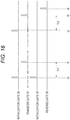
- the reading control unit 53 controls each gate as shown in Fig. 16 , thereby implementing exposure corresponding to the plurality of light emissions as shown in Fig. 14 .
- the reading control unit 53 causes the initialization gates 55 and 56 to initialize the photoelectric conversion unit 51 and the charge holding unit 52.
- exposure is performed by the photoelectric conversion unit 51 as the exposure period Tr1.
- the reading control unit 53 controls the transfer gate 57 to transfer the charge of each pixel accumulated in the photoelectric conversion unit 51 in the exposure period Tr1 to the charge holding unit 52.
- the reading control unit 53 does not open the reading gate 58 such that the charge transferred from the photoelectric conversion unit 51 is held in the charge holding unit 52.
- the reading control unit 53 controls the initialization gate 55 to initialize the photoelectric conversion unit 51. At this time, the charge holding unit 52 is not initialized.
- the reading control unit 53 controls the transfer gate 57 to transfer the charge of each pixel accumulated in the photoelectric conversion unit 51 in the exposure period Tr2 to the charge holding unit 52.
- the charge holding unit 52 holds the charge of the exposure period Tr2 in addition to the exposure period Tr1.
- the reading control unit 53 controls the reading gate 58 at time point t4 to output the charge of each pixel held in the charge holding unit 52 to the reading amplifier 54.
- the charges caused by two exposures of the exposure periods Tr1 and Tr2 are output as each pixel data of one-frame captured data DT constituting one piece of image.
- Fig. 14 shows an example of performing two light emissions and exposures in one frame period Tf, but of course this is not limited to two.
- Fig. 17 shows a case where three light emissions are performed in one frame period Tf. That is, the light emitting elements 2a perform light emissions of light emission periods Tp1, Tp2, and Tp3, and the image sensor 7 performs exposures of exposure periods Tr1, Tr2, and Tr3.
- one continuous light emission and exposure in one frame period Tf are performed.
- this is an operation to switch, for example, between two light emissions and exposures and three light emission and exposures as needed.
- the exposure time is set at a value within a certain threshold, two light emissions and exposures are performed, and when the exposure time is desired to be longer than the threshold, three light emissions and exposures are performed, and the like.
- two or three light emissions and exposures is one example, and two or three or more light emissions and exposures may be performed.
- the emission interval may be controlled to ensure that the temperature drops.
- the minimum length is secured as the light emission interval (non-light emission period), the temperature detection signal by the temperature detecting unit 10 is confirmed to shift to the next light emission period Tp on condition that the temperature falls to a predetermined temperature or lower, and the like.
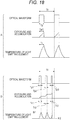
- Fig. 18A shows a case of performing one light emission and exposure in one frame period Tf as shown in Fig. 13 above. That is, continuous light emission and exposure are performed in one frame period Tf with a light emission period Tp and an exposure period Tr. Temperature rise of light emitting elements 2a is relatively high.
- Fig. 18B shows a state where the temperature rise of the light emitting elements 2a is inhibited by suspending and resuming light emission and exposure according to the temperature.
- Fig. 18B in one frame period Tf, three divided light emissions and exposures are performed as light emission periods Tp1, Tp2, and Tp3, and exposure periods Tr1, Tr2, and Tr3.
- a drive unit 3 or a control unit 9 monitors the temperature by a temperature detecting unit 10 in the light emission period Tp1 and controls the drive of the light emitting elements 2a.
- the light emission of the light emitting elements 2a by the drive unit 3 is suspended. Thereafter, when it is detected that the temperature of the light emitting elements 2a drops to a temperature threshold th2, the light emission of the light emitting elements 2a by the drive unit 3 is resumed. That is, the light emission period Tp2 is started.
- the light emission period Tp2 is suspended when the temperature of the light emitting elements 2a reaches the temperature threshold th1. Furthermore, thereafter, when it is detected that the temperature of the light emitting elements 2a drops to the temperature threshold th2, the light emitting is resumed. That is, the light emission period Tp3 is started.
- the length of the light emission period Tp of Fig. 18A is a light emission period length TpG
- the light emission period Tp3 is finished when the total light emission time of the light emission periods Tp1, Tp2, and Tp3 reaches the light emission period length TpG.
- the exposure periods Tr1, Tr2, and Tr3 in an image sensor 7 are controlled in synchronization with the light emission periods Tp1, Tp2, and Tp3, respectively.
- the figure shows an example in which three light emissions and exposures are performed, but this is not limited to three times because light emission is suspended and resumed and the light emission period length TpG is managed according to the temperature condition. It is also considered that the number of light emissions and exposures varies depending on the temperature condition at that time.
- Such control of suspension and resumption of light emission may be performed by, for example, a logic circuit in the drive unit 3 and the like according to a detection signal by the temperature detecting unit 10, and the timing thereof may be transmitted to the image sensor 7.
- the control unit 9 may monitor the temperature detection signal by the temperature detecting unit 10 to synchronously control the drive unit 3 and the image sensor 7.
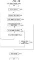
- Fig. 19 shows a processing example in which, for example, the control unit 9 controls the timing of suspending, resuming, and finishing light emission within one frame period Tf.
- the drive unit 3 may perform similar processing.
- step S101 of Fig. 19 to begin with, the control unit 9 sets the light emission period length TpG, which is the total light emission time in one frame period Tf.
- control unit 9 proceeds from step S102 to S103 every time the start timing of one frame is detected from a frame synchronization signal.
- step S103 the control unit 9 instructs the drive unit 3 to start emitting light from a light emitting unit 2. Furthermore, the control unit 9 starts counting the light emission time in step S104.
- step S105 the control unit 9 confirms whether or not the value of the light emission time being counted reaches the light emission period length TpG.
- step S106 the control unit 9 checks the temperature detection signal by the temperature detecting unit 10 and confirms whether or not the current temperature (temperature of the light emitting elements 2a) TMP is equal to or higher than the temperature threshold th1.
- control unit 9 continues monitoring of steps S105 and S106.
- control unit 9 proceeds from step S106 to S107 to control light emission suspension. That is, the control unit 9 causes the drive unit 3 to suspend the light emission of the light emitting unit 2, and instructs the image sensor 7 to suspend the exposure.
- control unit 9 After performing the light emission suspension control, the control unit 9 checks the temperature detection signal by the temperature detecting unit 10 in step S108, and confirms whether or not the current temperature TMP is equal to or lower than the temperature threshold th2. Until the current temperature TMP drops equal to or lower than the temperature threshold th2, the suspended state will continue as it is.
- control unit 9 proceeds from step S108 to S109 to control light emission resumption. That is, the control unit 9 causes the drive unit 3 to resume the light emission of the light emitting unit 2, and instructs the image sensor 7 to resume the exposure.
- control unit 9 returns to the monitoring of steps S105 and S106.
- step S105 If it is detected that the value of the light emission time being counted in step S105 reaches the light emission period length TpG, the control unit 9 proceeds to step S110 and instructs the drive unit 3 and the image sensor 7 to finish the light emission and exposure within the current frame period Tf.
- control unit 9 resets a light emission time counter, returns to step S102, and waits for start timing of the next frame.
- step S112 the control of Fig. 19 is finished at the time point.
- control unit 9 changes the light emission period length TpG accordingly.
- control unit 9 changes the light emission period length TpG due to various reasons, the control unit 9 returns from step S113 to S101 and changes the setting of the light emission period length TpG.
- one light emission duration time is controlled according to the temperature condition.
- the operation of performing a plurality of light emissions and exposures in one frame period Tf is performed.
- the temperature thresholds th1 and th2 are preferably set appropriately such that such a situation does not occur.
- one frame period Tf of image capturing does not necessarily have to be fixed, one frame period Tf may be variable and the control of Fig. 19 according to the current temperature TMP may be prioritized.
- control unit 9 An example of control by the control unit 9 will be described in Fig. 20A .
- step S150 the control unit 9 starts light emission and exposure as one light emission in one frame period Tf.
- flags FT1 and FT2 which will be described later, are turned off.
- the flag FT1 is a flag indicating a state in which two light emissions are being performed
- the flag FT2 is a flag indicating a state in which three light emissions are being performed.
- the control unit 9 monitors the finish of sensing in step S151.
- step S152 the control unit 9 checks the current temperature TMP (temperature of the light emitting elements 2a) from the temperature detection signal by the temperature detecting unit 10.
- control unit 9 performs processing of monitoring the current temperature or flag status.
- step S153 it is confirmed whether or not the current temperature TMP is equal to or higher than a certain temperature threshold th20 when the flag FT2 is off.
- step S154 it is confirmed whether or not the flag FT2 is turned on.
- step S155 it is confirmed whether or not the current temperature TMP is equal to or higher than a certain temperature threshold th10 when the flag FT1 is off.
- step S156 it is confirmed whether or not the flag FT1 is turned on.
- control unit 9 proceeds from step S155 to S164, and performs control to switch to the operation of performing two light emissions in one frame period Tf.
- control unit 9 instructs the drive unit 3 to perform two light emissions of the light emission periods Tp1 and TP2 as in Fig. 14 , and instructs the image sensor 7 to perform two exposures of the exposure periods Tr1 and Tr2.
- step S165 the control unit 9 turns on the flag FT1.
- control unit 9 monitors step S153 or S156.
- control unit 9 proceeds from step S156 to S166 to determine whether or not the current temperature TMP is equal to or lower than a temperature threshold th10u.
- the temperature threshold th10u is a temperature slightly lower than the temperature threshold th10 for shifting to two light emissions as shown in Fig. 20B .
- control unit 9 proceeds to step S167, and performs control to switch to one light emission in one frame period Tf.
- control unit 9 instructs the drive unit 3 to perform one light emission of the light emission period Tp as in Fig. 13 , and instructs the image sensor 7 to perform exposure of the exposure period Tr.
- step S168 the control unit 9 turns off the flag FT1.
- the temperature threshold th10u is slightly lower than the temperature threshold th10, a situation where two light emissions and one light emission are frequently switched is prevented.
- the control unit 9 monitors in step S153 whether or not the current temperature TMP is equal to or higher than the temperature threshold th20.
- the temperature threshold th20 is a temperature higher than the temperature threshold th10, as shown in Fig. 20B .
- control unit 9 proceeds from step S153 to S160, and performs control to switch to three light emissions in one frame period Tf.
- control unit 9 instructs the drive unit 3 to perform three light emissions of the light emission periods Tp1, Tp2, and Tp3 as in Fig. 17 , and instructs the image sensor 7 to perform three exposures of the exposure periods Tr1, Tr2, and Tr3.
- step S161 the control unit 9 turns on the flag FT2.
- control unit 9 monitors step S154.
- control unit 9 proceeds from step S154 to S162 to determine whether or not the current temperature TMP is equal to or lower than a temperature threshold th20u.
- the temperature threshold th20u is a temperature slightly lower than the temperature threshold th20 for shifting to three light emissions as shown in Fig. 20B .
- the control unit 9 turns off the flag FT2 in step S163 and further proceeds to step S164, and performs control to switch to two light emissions in one frame period Tf. That is, the control unit 9 returns from three light emissions to two light emissions. At this time, if the flag FT1 is off, the flag FT1 will be turned on in step S165.
- the temperature threshold th20u is slightly lower than the temperature threshold th20, a situation where three light emissions and two light emissions are frequently switched is prevented.
- the control unit 9 finishes the processing of Fig. 20A from step S151.
- the distance measuring device 1 by controlling the light emission interval, the light emission duration time per time, and the number of light emissions at the timing of a plurality of light emissions or exposures performed to obtain one-time image, it is possible to inhibit heat generation of the light source and improve power efficiency.
- Fig. 21A shows an example in which a light emitting unit 2 performs, for example, four light emissions (light emission periods Tp1, Tp2, Tp3, Tp4) in one frame period Tf as shown as an optical waveform.
- Fig. 21A shows how an amount of accumulated charge increases as an exposure operation of pixels G1 and G2 in accordance with a light emission operation.
- exposure of exposure periods Tr1 and Tr2 is performed in accordance with the light emission periods Tp1 and Tp2. However, no exposure is performed in the light emission periods Tp3 and Tp4.
- exposure of exposure periods Tr1, Tr2, Tr3, and Tr4 is performed in accordance with the light emission periods Tp1, Tp2, Tp3, and Tp4.
- the pixel G1 is, for example, as shown in Fig. 21B , a pixel near the center of an image capturing surface of the image sensor 7 (photoelectric conversion unit 51) and having relatively high sensitivity.
- the pixel G2 is, for example, a pixel near a screen end of the image capturing surface and having relatively low sensitivity.
- the number of exposures to a plurality of light emissions can be set according to the pixel. This makes it possible, even in a case where there is a difference in pixel sensitivity, to obtain captured data in which any pixel is in a good luminance range.
- the pixel sensitivity is affected not only by the characteristics of the pixel but also by the characteristics of a light emitting element 2a.
- the degree of temperature rise is greater near the center of the light emitting unit 2 than in an end.
- a laser light emitting element as VCSEL has a characteristic that power decreases as the temperature rises. Therefore, the amount of light of the light emitting element 2a may drop as disposed closer to the central portion.
- the luminance may drop near the center of the image capturing surface of the image sensor 7. In such a case, it is considered to increase the number of exposures in the pixel G1 near the center.
- Fig. 21A also shows an example as a pixel G3, and in this case, in the exposure period Tr3, the exposure is finished in the middle of the light emission period Tp3.
- a distance measuring device 1 in synchronization with a plurality of light emissions of the light source device 100, by individually controlling the exposure duration time and the number of exposures per one time for each pixel or each block including a number of pixels in the image capturing surface of the image sensor 7, it is possible to configure a distance measuring device 1 to control the luminance of the reflected light image of the light source reflected by the subject S on the image captured by the image sensor 7.
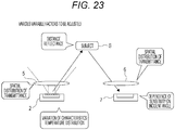
- a distance measuring device 1 in which a light source device 100 causes a large number of light emitting elements 2a to emit light and reflected light thereof is captured by an image capturing device 101 to measure a distance, luminance of a bright spot on an obtained image is not always uniform due to manufacturing variations of lasers (light emitting elements 2a), temperature fluctuations, and optical system characteristics.
- the light emitting elements X and Y are samples of certain two light emitting elements 2a referred to in the description among the large number of light emitting elements 2a.
- Fig. 22A shows that light emission intensity PW1 and PW2 cannot be equalized due to manufacturing variations, temperature distribution, parasitic resistance, and the like even though driving of the light emitting elements X and Y are controlled with the same parameter.
- the factors include spatial distribution of transmittance of a light emission side optical system 5, a distance from the distance measuring device 1 to a subject S, reflectance of the subject S, spatial distribution of transmittance of an image capturing side optical system 6, dependence of sensitivity of the image sensor 7 on an incident angle, and the like.
- Fig. 22B schematically shows how the image sensor 7 captures reflected light of the subject S illuminated in such a situation. As shown in the figure, each pixel (or each pixel block) appears as a variation in brightness.
- each of multi-lamp light sources or each block including a plurality of light sources by controlling lighting start time, lighting end time, or a current amount so as to differ depending on the situation, luminance of reflected light on the captured image is adjusted to a desired amount.
- two-dimensionally distributed light sources are captured as a two-dimensional image with the image sensor 7, and the current or light emission time or both of each block of the light sources are controlled such that brightness in the image becomes a desired state.
- the light emission side optical system 5, the subject S, and an image capturing side optical system 6 are on the optical path from a light emitting unit 2 to the image sensor 7, it is possible to perform control considering not only the manufacturing variation of the multi-lamp light source but also the variation caused by each component on the optical path described above.
- an idea of the present embodiment is to perform control, not to aim to shine at desired brightness in the light emitting unit 2, but to appear in a desired way on the image sensor 7 side.
- Fig. 22C shows one example of individually controlling the light emission timings of the light emitting elements X and Y.
- Light emission of the light emitting element X is controlled by start timing Tst1 and end timing Ted1.
- Light emission of the light emitting element Y is controlled by start timing Tst2 and end timing Ted2.
- the lengths of light emission periods TpX and TpY of the light emitting elements X and Y are different from each other.
- the light emission timings of the light emitting elements X and Y are controlled such that the luminance variation between pixels of the captured data does not occur.
- Fig. 22C is one example.
- Fig. 24 shows various control examples.
- Fig. 24A is an example of causing the light emitting elements X and Y to emit light at the same start timing Tst and end timing Ted for comparison.
- Fig. 24B is an example in which the start timings Tst1 and Tst2 of the light emitting elements X and Y are shifted, and the end timings Ted1 and Ted2 are shifted.
- the light emission periods TpX and TpY of the light emitting elements X and Y can be made different depending on an amount of timing shift.
- Fig. 24C is an example in which the start timing Tst is common to the light emitting elements X and Y, but the end timings Ted1 and Ted2 are different timings as needed.
- Fig. 24D is an example in which the start timings Tst1 and Tst2 are fixedly shifted and the end timings Ted1 and Ted2 are different timings as needed in the light emitting elements X and Y.
- parameter setting it is also considered to perform a plurality of light emissions and exposures in one frame period Tf as described in the first to third embodiments.
- timing control with the light emission parameter timing setting for a plurality of light emissions is also assumed.
- An operation of the fourth embodiment as described above is to variably control the parameter to be given to the drive unit 3 for laser light emission according to the captured data on the image sensor 7 side.
- Static parameter control and dynamic parameter control can be considered as a method of parameter control.
- the static parameter control is to perform calibration according to a fixed situation to set the parameter.
- the light emitting elements X and Y emit light with the same parameter. That is, light emission is driven by using the same values (same light emission period Tp) as the laser power, the start timing Tst, and the end timing Ted.
- the parameters of the light emitting elements X and Y are set individually so as to resolve the luminance variation.
- the current values are set differently, or the timing parameters are changed to make the light emission periods TpX and TpY different from each other.
- the dynamic parameter control is to adaptively set the parameters variably according to the situation changing during sensing.
- the parameters of the light emitting elements X and Y are determined according to the initial temperature distribution of the light emitting unit 2 to emit light. Note that it can be considered that after the static parameter control is performed, the parameter setting according to the initial temperature distribution is included therein.
- the parameters of the light emitting elements X and Y are set individually so as to resolve the luminance variation.
- the current values are set differently, or the timing parameters are changed to make the light emission periods TpX and TpY different from each other.
- the exposure period cannot be variably controlled for each individual pixel (or block pixel) on the image sensor 7 side, it is considered to set the exposure period to perform exposure in the period from the earliest start timing Tst to the latest end timing Ted among the earliest parameters for the plurality of light emitting elements 2a.
- control unit 9 may be a separate body from the drive unit 3 or may be provided within the drive unit 3.
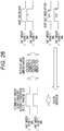
- control unit 9 performs the above-described static parameter control in step S10 as static calibration.
- step S11 the control unit 9 controls the drive unit 3 and the image sensor 7 such that the light emitting unit 2 starts light emission and the image sensor 7 starts image capturing on the basis of the parameter adjusted by the static calibration.
- control unit 9 finishes the processing from step S12.
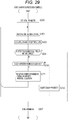
- Fig. 27 is a processing example to perform only the static parameter control.
- step S200 the control unit 9 sets an initial parameter for the drive unit 3 and the image sensor 7. This is a parameter that designates the laser power and the light emission period Tp common to all the plurality of light emitting elements 2a.
- the initial parameter may be a parameter obtained by shifting the start timing Tst and the end timing Ted.
- the initial parameter also includes a gain to be given to an image capturing signal on the image sensor 7 side and the exposure period Tr.
- the exposure period Tr is synchronized with the light emission period Tp.
- control unit 9 performs light emission control in step S201. That is, the control unit 9 causes the drive unit 3 to start light emission, and causes the image sensor 7 to start exposure synchronized with the light emission.
- captured data is obtained on the image capturing device 101 side, and the control unit 9 enters a state where information on the captured data, that is, luminance data in each pixel or pixel block can be checked.
- step S202 the control unit 9 acquires the luminance value of each pixel of the captured data.
- step S203 the control unit 9 confirms whether or not the pixel value (luminance value) can be detected in all the pixels required for distance measurement sensing.
- all the pixels required for sensing mean all the pixels that should receive the reflected light from the laser light emission, and do not necessarily refer to all the pixels physically provided in the image sensor 7.
- all the pixels are used in such meaning.
- step S203 the control unit 9 confirms whether or not at least light reception within a dynamic range of the image sensor 7 can be implemented in all the pixels.
- the pixel value is not saturated and is not buried in noise, and an appropriate pixel value is obtained, at least the sensing operation is possible, and thus it is only required that light reception can be implemented within the dynamic range.
- step S203 conditions may be defined more strictly that all the pixels are within a predetermined luminance value range.
- control unit 9 stores the current parameter in step S207 and finishes the static calibration. For example, in a case where there is no problem with the initial parameter, the static calibration will be finished with the initial parameter as it is.
- control unit 9 proceeds to step S204 to determine whether or not the sensor parameter is adjustable.
- the gain to be given to the image capturing signal in the image sensor 7 is adjustable.
- control unit 9 proceeds to step S205 to change one or both of the gain or the exposure period.
- steps S201, S202, and S203 are performed to determine whether or not proper pixel detection is implemented.
- step S203 the fact that all the pixels can be properly detected in step S203 means that the adjustment has been performed, particularly without the need to control the parameter of each light emitting element 2a individually.
- step S207 the control unit 9 stores the parameter in the state after adjusting the sensor parameter as the parameter after the static calibration.
- step S204 it may be determined in step S204 that the sensor parameter cannot be changed. This is a case, for example, where the gain or exposure time has reached the upper limit or lower limit that is determined in advance as a variable range.
- control unit 9 proceeds to step S206 to make individual light emission parameter adjustment.
- control unit 9 changes the light emission parameter as shown in Figs. 22C and 24 .
- the light emission parameter is set according to the variation in the luminance of captured data.
- the light emission parameter is set such that, for example, for the light emitting element 2a corresponding to a pixel (or pixel block) with insufficient luminance, the light emission period Tp is set long, and for the light emitting element 2a corresponding to a pixel (or pixel block) with too high luminance (or saturated), the light emission period Tp is set short.
- parameter setting will be performed to perform a plurality of light emissions (and exposures) in one frame period Tf.
- the parameter of the laser power may be set individually.
- steps S201, S202, and S203 is performed with the set parameter to determine whether or not appropriate pixel detection is implemented.
- step S203 the control unit 9 proceeds to step S207, and stores the light emission parameter and the sensor parameter at that time point as parameters of the static calibration result.
- the processing load is reduced by giving priority to overall control with simple parameter setting. Meanwhile, large variations can be handled by making individual setting.
- step S203 determines whether or not the luminance values of all the pixels cannot be properly detected.
- the control unit 9 confirms in step S210 whether or not the light emission parameter is adjustable. Then, if adjustable, the control unit 9 proceeds to step S211 to make overall adjustment or individual adjustment to the light emission parameter. Then, the control unit 9 performs processing of steps S201, S202, and S203.
- step S210 the control unit 9 proceeds to step S212 to adjust the sensor parameter.
- the gain adjustment in the image sensor 7 is performed.
- step S203A has stricter conditions than step S203. That is, the condition does not mean that only all the pixels can be detected properly, but means that the luminance value of all the pixels is within a predetermined range. This means adjusting the parameter until the variation decreases.
- step S220 the control unit 9 changes the light emission parameter such that the laser power is reduced by one step for all the light emitting elements 2a.
- one step here means one-step reduction amount set for the processing of step S220, and is not necessarily limited to a variable amount in terms of resolution of the laser power (drive current value) that can be set.
- step S221 the control unit 9 controls the drive unit 3 such that the light emitting elements 2a emit light according to the changed light emission parameter, and in step S222, the control unit 9 acquires the luminance value of each pixel of the captured data captured corresponding to the light emission.
- step S223 the control unit 9 determines whether or not all the pixels are detected with the luminance value equal to or higher than a predetermined value.
- the predetermined value is a luminance value at a level at which there is no problem in image detection and distance measurement sensing.
- control unit 9 returns to step S207 and stores the current parameter including the laser power reduced in the immediately preceding step S220.
- step S220 the control unit 9 further reduces the laser power by one step, and performs the processing of steps S221, S222, and S223.
- the laser power is reduced.
- step S223 If the luminance value of some pixel becomes less than the predetermined value in step S223, the process is finished at the time point.
- the parameter stored at this time is a parameter in a case where the luminance value becomes equal to or higher than the predetermined value in all the pixels immediately before the luminance value becomes less than the predetermined value in some pixel. That is, the parameter indicates a state where the laser power is reduced as much as possible.
- the static calibration is to reduce the laser power as much as possible while inhibiting the luminance variation in each pixel of the captured data as much as possible (inhibit to the appropriate range in step S203A).
- the predetermined value used as a threshold in step S223 is preferably set with a certain margin from a value at which detection becomes impossible.
- the laser power can be reduced as much as possible within the range where appropriate sensing can be performed, and power consumption can be reduced and luminous efficiency can be improved.
- Fig. 30 is based on the processing of Fig. 28 with steps S220 to S223 added, but a processing example based on the processing of Fig. 29 with steps S220 to S223 added can also be considered.
- step S10 in the first example of the parameter setting processing of Fig. 27 .
- a second example as parameter setting processing in which such static calibration processing examples I, II, and III can be adopted will be described subsequently.
- Fig. 31 shows a second example of parameter setting processing.
- control unit 9 performs the static calibration in step S10, and then measures the temperature in step S21. That is, the control unit 9 checks the current temperature TMP from the temperature detection signal by a temperature detecting unit 10.
- control unit 9 performs calibration according to the temperature in step S22.
- step S23 the control unit 9 controls the drive unit 3 and the image sensor 7 such that the light emitting unit 2 starts light emission and the image sensor 7 starts image capturing on the basis of the parameter adjusted by the static calibration and the further calibration according to the temperature.
- steps S21, S22, and S23 are continuously performed, and when the sensing is finished, the control unit 9 finishes the processing from step S12.
- Fig. 31 is an example of performing temperature calibration as the dynamic parameter control in addition to the static parameter control.
- the temperature calibration in step S22 is, for example, to control the laser power (drive current amount) according to the current temperature TMP.
- the drive current amount may be changed as overall control for all the light emitting elements 2a, but the drive current amount may be controlled individually (for each block) according to the temperature distribution.
- the parameter may be set so as to perform a divided plurality of light emissions within one frame described above.
- the temperature rise is not promoted while ensuring the amount of light.
- Steps S10, S21, S22 and S23 are similar to Fig. 31 .
- the control unit 9 adjusts one or both of the light emission parameter and the sensor parameter in step S24 according to the brightness appeared in the captured data.
- steps S21, S22, S23, and S24 are continuously performed, and when sensing is finished, the control unit 9 finishes the processing from step S12.
- Fig. 32 is an example of performing temperature calibration and calibration according to reflectance of the subject S as dynamic parameter control in addition to static parameter control.
- the light emission period and the laser power are controlled within a non-saturating range according to the change in the reflectance and the distance of the subject S.
- This can be an overall adjustment of the light emitting elements 2a or individual adjustment.
- the light emission period Tp is shortened for the corresponding light emitting element 2a, and the like.
- gain adjustment and exposure period adjustment are performed within a non-saturating range according to the change in the reflectance and the distance of the subject S.
- the static parameter control and the dynamic parameter control are performed by the above various processing examples, whereby captured data with little luminance variation can be obtained and the sensing precision can be improved.
- a light source device 100 includes: a plurality of laser light emitting elements 2a; and a drive unit 3 configured to drive each of the laser light emitting elements 2a to perform a plurality of light emissions in one frame period in an image sensor 7 that receives and captures light emitted from the plurality of laser light emitting elements 2a and reflected by a subject S.
- the period length in which laser light emission is continuously performed is divided into a plurality of times and laser light emission is performed, the temperature rise in each light emission period Tp is inhibited, and the temperature drop occurs in a non-light emission period. That is, even if the light emission is performed for the same period length integrally, a plurality of light emissions allows the temperature rise to be inhibited more than in a case where light emission is performed continuously.
- the technology of the embodiments enables calculation of a distance and the like from one piece of image obtained by accumulating a plurality of light emissions, and the exposure period on the image sensor 7 side can be adjusted on the image sensor 7 side.
- This brings an advantage that light emission with an arbitrary cycle and pulse width can be used on the light source device side according to conditions such as heat generation and ambient temperature.
- the drive unit 3 changes the number of light emissions of the laser light emitting elements 2a in one frame period according to a temperature detection result (see Figs. 19 and 20 ) .
- the temperature rise can be effectively inhibited, but it may be advantageous to continuously perform laser light emission and to continuously perform exposure on the image sensor 7 side in terms of lighter processing load.
- one light emission is performed in one frame period. Then, when necessary, switching is performed to a plurality of light emissions in one frame. This enables inhibition of temperature rise and appropriate sensing continuously.
- the drive unit 3 changes the number of light emissions of the laser light emitting elements 2a as a plurality of light emissions in one frame period according to a temperature detection result (see Fig. 20 ).
- the number of emissions as the plurality of light emissions is switched, such as two light emissions or three light emissions in one frame period.
- the light emission period length, emission interval, and the like differ depending on the number of light emissions in one frame period, the effect of inhibiting the temperature rise can be made different. Therefore, even in a case where a plurality of light emissions is used, the number of light emissions is switched according to temperature conditions.
- the effect of inhibiting the temperature rise can be gradually increased to maintain a normal state.
- the laser light emitting elements 2a include vertical cavity surface emitting lasers (VCSEL).
- VCSEL vertical cavity surface emitting lasers
- the technology of the present disclosure can be applied not only to VCSEL but also to light source devices equipped with other types of laser light emitting elements.
- the light source device 100 further includes a temperature sensor 10a (temperature detecting unit 10) configured to detect a temperature near the laser light emitting elements 2a.
- a temperature sensor 10a temperature detecting unit 10
- the temperature sensor 10a is disposed near the laser light emitting elements 2a as VCSEL.
- the temperature of the laser light emitting elements 2a (for example, mesa temperature near the laser light emitting elements 2a) can be obtained, and the appropriate number of light emissions can be controlled accordingly.
- the temperature distribution on a light emitting surface can also be detected by disposing the temperature sensor 10a. With this configuration, it is considered to control driving at a different number of light emissions according to locations where the laser light emitting elements 2a are arranged in the plane.
- a temperature sensor 10a configured to detect a temperature near the laser light emitting elements 2a is further provided, and the drive unit 3 performs light emission suspension and light emission resumption of the laser light emitting elements in one frame period according to a detection result of the temperature sensor 10a.
- a plurality of light emissions of the laser light emitting elements 2a according to the temperature condition will be performed.
- the temperature condition as a reference for suspending and resuming light emission, this is suitable for the purpose of controlling the temperature.
- the drive unit 3 drives each of the laser light emitting elements according to a light emission parameter that defines a light emission operation of the laser light emitting elements 2a per predetermined unit.
- the drive unit 3 can flexibly perform laser control according to various circumstances because of the configuration that allows driving with the light emission parameter set for each of the light emitting elements 2a of the predetermined unit. For example, it is possible to perform control such as performing a plurality of light emissions in one frame only for the laser light emitting element 2a of a specific block. For example, in a case where in-plane distribution is detected by the temperature sensor 10a, it is possible to make the temperature uniform by performing a plurality of light emissions only for some of the laser light emitting elements 2a accordingly, and the like.
- the light source device 100 has a configuration in which the drive unit 3 drives each of the laser light emitting elements according to a light emission parameter that defines a light emission operation of the laser light emitting elements 2a, and the light source device 100 includes a control unit 9 configured to generate the light emission parameter.
- control unit 9 is provided in the light source device 100 (for example, in a chip as the light source device 100).
- control unit 9 is integrated with the light emitting unit 2 and the drive unit 3 as the light source device 100 (for example, in the same chip), it is possible to have a configuration advantageous for setting and transferring the light emission parameter.
- the drive unit 3 controls duration time (light emission periods Tp1, Tp2, ...) of one light emission of the plurality of light emissions with a set light emission parameter.
- a temperature rise occurs during the light emission period.
- the drive unit 3 controls a light emission interval (non-light emission period) of the plurality of light emissions with a set light emission parameter.
- the non-light emission period is a period in which the temperature drops.
- An image sensor 7 includes a photoelectric conversion unit 51 configured, in a case where a plurality of laser light emitting elements 2a of a light source device 100 performs a plurality of light emissions in one frame period in which a captured image is generated, to perform exposure to light emitted from the laser light emitting elements 2a and reflected by a subject S in an exposure period Tr corresponding to a period Tp of each of the plurality of light emissions. Then, one-frame captured data obtained by a plurality of exposures is output.
- the image capturing device 101 will also perform a collaboration operation.
- the luminance on the captured image can be controlled to a desired value, and for example, it is possible to provide the image capturing device that can accurately perform image capturing for distance measurement, 3D shape estimation of an object, and the like.
- the image sensor 7 further includes a charge holding unit 52 configured to hold a charge by the exposure of the photoelectric conversion unit 51 according to the period of each of the plurality of light emissions of the laser light emitting elements 2a in one frame period, and a charge signal that generates one image in each frame period is read from the charge holding unit 52 (see Fig. 15 ).
- the distance and the like can be calculated from one piece of image obtained by accumulating the plurality of light emissions.
- the photoelectric conversion unit 51 allows settings of an operation of performing exposure corresponding to a period of each of the plurality of light emissions in one frame, and an operation of performing exposure corresponding to a period of a part of the plurality of light emissions.
- the operation of performing exposure corresponding to a period of each of the plurality of light emissions of the laser light emitting elements and the operation of performing exposure in a period of a part of the plurality of light emissions can be selectively performed.
- the luminance of the captured data can be made uniform, and improvement in detection precision can be promoted.
- the image sensor 7 of the embodiments does not need to make the exposure duration time per one time and the number of exposures identical to those on the light emitting side. Therefore, it is possible to control these individually within the image sensor plane, and it is possible to control the bright spot caused by the reflected light of the light source in the obtained image to have desired luminance.
- the photoelectric conversion unit 51 may be configured to set the number of exposures corresponding to a period of each of the plurality of light emissions in one frame per predetermined pixel unit.
- the operation of performing exposure every time corresponding to a period of each of the plurality of light emissions of the laser light emitting elements 2a and the operation of performing exposure in a period of a part of the plurality of light emissions can be selectively performed per predetermined pixel unit.
- the predetermined pixel unit mentioned here is a unit of one pixel, a unit of a blocked plurality of pixels, and the like.
- the exposure time can be changed in the image capturing surface of the image sensor 7, and the luminance of the obtained image can be controlled to be desired luminance.
- the distance measuring device 1 of the embodiments can be configured as a sensing module.
- This sensing module includes: a plurality of laser light emitting elements 2a; a drive unit 3 configured to drive each of the laser light emitting elements 2a to perform a plurality of light emissions in one frame period in an image sensor 7 that receives and captures light emitted from the plurality of laser light emitting elements 2a and reflected by a subject S; and the image sensor 7 including a photoelectric conversion unit 51 configured to perform exposure to the light emitted from the laser light emitting elements 2a and reflected by the subject in an exposure period corresponding to a period of each of the plurality of light emissions, the image sensor 7 outputting one-frame captured data obtained by a plurality of the exposures.
- the sensing module that performs distance measurement, object recognition, and the like is implemented.
- the light source performs a plurality of light emissions in order to obtain one-time captured image
- the 3D shape of the object is estimated by using one piece of captured image generated by accumulating the reflected light a plurality of times, and sensing precision can be improved by performing sufficient exposure while inhibiting the temperature rise.
- the sensing module includes a temperature sensor 10a (temperature detecting unit 10) configured to detect a temperature near the laser light emitting elements 2a.
- the drive unit 3 changes the number of light emissions of the laser light emitting elements in one frame period according to a temperature detection result by the temperature sensor 10a.
Landscapes
- Physics & Mathematics (AREA)
- General Physics & Mathematics (AREA)
- Engineering & Computer Science (AREA)
- Electromagnetism (AREA)
- Condensed Matter Physics & Semiconductors (AREA)
- Optics & Photonics (AREA)
- Remote Sensing (AREA)
- Computer Networks & Wireless Communication (AREA)
- Radar, Positioning & Navigation (AREA)
- Multimedia (AREA)
- Signal Processing (AREA)
- Computer Vision & Pattern Recognition (AREA)
- Optical Radar Systems And Details Thereof (AREA)
- Transforming Light Signals Into Electric Signals (AREA)
- Semiconductor Lasers (AREA)
- Measurement Of Optical Distance (AREA)
- Studio Devices (AREA)
Applications Claiming Priority (2)
| Application Number | Priority Date | Filing Date | Title |
|---|---|---|---|
| JP2018144925A JP2020020681A (ja) | 2018-08-01 | 2018-08-01 | 光源装置、イメージセンサ、センシングモジュール |
| PCT/JP2019/023867 WO2020026616A1 (ja) | 2018-08-01 | 2019-06-17 | 光源装置、イメージセンサ、センシングモジュール |
Publications (3)
| Publication Number | Publication Date |
|---|---|
| EP3832253A1 true EP3832253A1 (de) | 2021-06-09 |
| EP3832253A4 EP3832253A4 (de) | 2021-09-15 |
| EP3832253B1 EP3832253B1 (de) | 2024-05-22 |
Family
ID=69232445
Family Applications (1)
| Application Number | Title | Priority Date | Filing Date |
|---|---|---|---|
| EP19844024.0A Active EP3832253B1 (de) | 2018-08-01 | 2019-06-17 | Lichtquellenvorrichtung, bildsensor und sensormodul |
Country Status (5)
| Country | Link |
|---|---|
| US (1) | US11743615B2 (de) |
| EP (1) | EP3832253B1 (de) |
| JP (1) | JP2020020681A (de) |
| CN (1) | CN112534206B (de) |
| WO (1) | WO2020026616A1 (de) |
Families Citing this family (8)
| Publication number | Priority date | Publication date | Assignee | Title |
|---|---|---|---|---|
| US12418638B2 (en) * | 2018-08-30 | 2025-09-16 | Symbotic Llc | Calibration of depth-sensing computer vision systems |
| US11710945B2 (en) | 2020-05-25 | 2023-07-25 | Apple Inc. | Projection of patterned and flood illumination |
| US11699715B1 (en) | 2020-09-06 | 2023-07-11 | Apple Inc. | Flip-chip mounting of optoelectronic chips |
| DE112022000204T5 (de) | 2021-03-26 | 2023-08-17 | Ams Sensors Belgium Bvba | Bildsensoranordnung, Bildsensorvorrichtung und Verfahren zum Betrieb einer Bildsensoranordnung |
| JP7753657B2 (ja) * | 2021-04-14 | 2025-10-15 | 富士フイルムビジネスイノベーション株式会社 | 発光装置及び計測装置 |
| JP7689346B2 (ja) * | 2021-10-06 | 2025-06-06 | パナソニックIpマネジメント株式会社 | 撮像素子および測距装置 |
| US12313812B2 (en) | 2022-09-20 | 2025-05-27 | Apple Inc. | MOE-based illumination projector |
| US12123589B1 (en) | 2023-05-22 | 2024-10-22 | Apple Inc. | Flood projector with microlens array |
Family Cites Families (13)
| Publication number | Priority date | Publication date | Assignee | Title |
|---|---|---|---|---|
| JP2568388B2 (ja) * | 1994-09-15 | 1997-01-08 | シーケーディ株式会社 | 形状計測装置 |
| JP3912816B2 (ja) * | 1996-05-13 | 2007-05-09 | キヤノン株式会社 | 走査露光装置及びそれを用いたデバイスの製造方法 |
| US6415241B1 (en) * | 1998-09-21 | 2002-07-02 | Fuji Photo Optical Co., Ltd. | Distance measurement system |
| JP3749638B2 (ja) * | 1998-09-21 | 2006-03-01 | フジノン株式会社 | 測距装置 |
| US9442186B2 (en) * | 2013-05-13 | 2016-09-13 | Microsoft Technology Licensing, Llc | Interference reduction for TOF systems |
| WO2015001770A1 (ja) | 2013-07-01 | 2015-01-08 | パナソニック インテレクチュアル プロパティ コーポレーション オブ アメリカ | 複数の光源を有するモーションセンサ装置 |
| JP6355066B2 (ja) | 2013-08-29 | 2018-07-11 | 株式会社リコー | センサ装置及び画像形成装置 |
| EP2955544B1 (de) | 2014-06-11 | 2020-06-17 | Sony Depthsensing Solutions N.V. | TOF-Kamerasystem und Verfahren zum Messen einer Entfernung mit dem System |
| WO2015199615A1 (en) * | 2014-06-27 | 2015-12-30 | Heptagon Micro Optics Pte. Ltd. | Structured light imaging system and method |
| DE112015003608T5 (de) * | 2014-08-05 | 2017-04-20 | Fujifilm Corporation | Abstandsmessvorrichtung, Abstandsmessverfahren und Abstandsmessprogramm |
| CN108431631A (zh) * | 2015-12-21 | 2018-08-21 | 株式会社小糸制作所 | 车辆用图像获取装置、控制装置、包括了车辆用图像获取装置或控制装置的车辆和车辆用图像获取方法 |
| US10459522B2 (en) * | 2016-06-15 | 2019-10-29 | Konkuk University Glocal Industry-Academic Collaboration Foundation | System and method for inducing somatic sense using air plasma and interface device using them |
| CN113466882B (zh) | 2017-07-05 | 2026-03-24 | 奥斯特公司 | 光测距装置 |
-
2018
- 2018-08-01 JP JP2018144925A patent/JP2020020681A/ja active Pending
-
2019
- 2019-06-17 CN CN201980049609.9A patent/CN112534206B/zh active Active
- 2019-06-17 EP EP19844024.0A patent/EP3832253B1/de active Active
- 2019-06-17 US US17/255,839 patent/US11743615B2/en active Active
- 2019-06-17 WO PCT/JP2019/023867 patent/WO2020026616A1/ja not_active Ceased
Also Published As
| Publication number | Publication date |
|---|---|
| CN112534206A (zh) | 2021-03-19 |
| CN112534206B (zh) | 2023-09-29 |
| EP3832253A4 (de) | 2021-09-15 |
| WO2020026616A1 (ja) | 2020-02-06 |
| US11743615B2 (en) | 2023-08-29 |
| EP3832253B1 (de) | 2024-05-22 |
| US20210258521A1 (en) | 2021-08-19 |
| JP2020020681A (ja) | 2020-02-06 |
Similar Documents
| Publication | Publication Date | Title |
|---|---|---|
| EP3832253B1 (de) | Lichtquellenvorrichtung, bildsensor und sensormodul | |
| EP3832252B1 (de) | Lichtquellenvorrichtung, bildgebungsvorrichtung und sensormodul | |
| WO2020044818A1 (ja) | 光源装置、調整方法、センシングモジュール | |
| US12206219B2 (en) | Light source apparatus, temperature detection method, and sensing module | |
| CN112640232B (zh) | 光源设备和感测模块 | |
| WO2020044817A1 (ja) | 光源装置、検出方法、センシングモジュール | |
| US20220276381A1 (en) | Laser drive device, sensing module, and timing adjustment method | |
| US12477840B2 (en) | Control circuit and distance measuring system | |
| JP4317413B2 (ja) | カメラモジュールおよび電子画像記録方法 | |
| KR102411963B1 (ko) | 전류 보상을 가진 전력 공급 시스템 | |
| US12088061B2 (en) | Light source device, drive method, and sensing module | |
| US12219274B2 (en) | Imaging device and imaging method | |
| JP2024108115A (ja) | 距離画像撮像装置、距離画像撮像方法、及びプログラム | |
| EP4513232A1 (de) | Halbleiterchip und verfahren zur einstellung einer belichtungszeit eines flugzeitsensors | |
| US12149046B2 (en) | Light emission drive circuit and light emission device | |
| CN115336125A (zh) | 驱动装置、发光装置以及驱动方法 | |
| TW202322501A (zh) | 發光裝置及測距裝置 | |
| US20230402819A1 (en) | Light emitting device and measuring device | |
| CN120529208A (zh) | 图像感测装置及其操作方法 |
Legal Events
| Date | Code | Title | Description |
|---|---|---|---|
| STAA | Information on the status of an ep patent application or granted ep patent |
Free format text: STATUS: THE INTERNATIONAL PUBLICATION HAS BEEN MADE |
|
| PUAI | Public reference made under article 153(3) epc to a published international application that has entered the european phase |
Free format text: ORIGINAL CODE: 0009012 |
|
| STAA | Information on the status of an ep patent application or granted ep patent |
Free format text: STATUS: REQUEST FOR EXAMINATION WAS MADE |
|
| 17P | Request for examination filed |
Effective date: 20201209 |
|
| AK | Designated contracting states |
Kind code of ref document: A1 Designated state(s): AL AT BE BG CH CY CZ DE DK EE ES FI FR GB GR HR HU IE IS IT LI LT LU LV MC MK MT NL NO PL PT RO RS SE SI SK SM TR |
|
| REG | Reference to a national code |
Ref country code: DE Ref legal event code: R079 Free format text: PREVIOUS MAIN CLASS: G01B0011000000 Ipc: G01B0011250000 Ref country code: DE Ref legal event code: R079 Ref document number: 602019052713 Country of ref document: DE Free format text: PREVIOUS MAIN CLASS: G01B0011000000 Ipc: G01B0011250000 |
|
| A4 | Supplementary search report drawn up and despatched |
Effective date: 20210816 |
|
| RIC1 | Information provided on ipc code assigned before grant |
Ipc: H01S 5/183 20060101ALN20210810BHEP Ipc: H01S 5/42 20060101ALI20210810BHEP Ipc: H01S 5/042 20060101ALI20210810BHEP Ipc: H04N 5/3745 20110101ALI20210810BHEP Ipc: H04N 5/369 20110101ALI20210810BHEP Ipc: H01S 5/062 20060101ALI20210810BHEP Ipc: G01C 3/06 20060101ALI20210810BHEP Ipc: G01B 11/25 20060101AFI20210810BHEP |
|
| DAV | Request for validation of the european patent (deleted) | ||
| DAX | Request for extension of the european patent (deleted) | ||
| STAA | Information on the status of an ep patent application or granted ep patent |
Free format text: STATUS: EXAMINATION IS IN PROGRESS |
|
| 17Q | First examination report despatched |
Effective date: 20230508 |
|
| GRAP | Despatch of communication of intention to grant a patent |
Free format text: ORIGINAL CODE: EPIDOSNIGR1 |
|
| STAA | Information on the status of an ep patent application or granted ep patent |
Free format text: STATUS: GRANT OF PATENT IS INTENDED |
|
| RIC1 | Information provided on ipc code assigned before grant |
Ipc: H01S 5/183 20060101ALN20240221BHEP Ipc: G01B 5/00 20060101ALI20240221BHEP Ipc: H01S 5/42 20060101ALI20240221BHEP Ipc: H01S 5/042 20060101ALI20240221BHEP Ipc: H01S 5/062 20060101ALI20240221BHEP Ipc: G01C 3/06 20060101ALI20240221BHEP Ipc: G01B 11/25 20060101AFI20240221BHEP |
|
| INTG | Intention to grant announced |
Effective date: 20240307 |
|
| GRAS | Grant fee paid |
Free format text: ORIGINAL CODE: EPIDOSNIGR3 |
|
| GRAA | (expected) grant |
Free format text: ORIGINAL CODE: 0009210 |
|
| STAA | Information on the status of an ep patent application or granted ep patent |
Free format text: STATUS: THE PATENT HAS BEEN GRANTED |
|
| P01 | Opt-out of the competence of the unified patent court (upc) registered |
Effective date: 20240409 |
|
| AK | Designated contracting states |
Kind code of ref document: B1 Designated state(s): AL AT BE BG CH CY CZ DE DK EE ES FI FR GB GR HR HU IE IS IT LI LT LU LV MC MK MT NL NO PL PT RO RS SE SI SK SM TR |
|
| REG | Reference to a national code |
Ref country code: GB Ref legal event code: FG4D |
|
| REG | Reference to a national code |
Ref country code: CH Ref legal event code: EP |
|
| REG | Reference to a national code |
Ref country code: DE Ref legal event code: R096 Ref document number: 602019052713 Country of ref document: DE |
|
| REG | Reference to a national code |
Ref country code: IE Ref legal event code: FG4D |
|
| REG | Reference to a national code |
Ref country code: LT Ref legal event code: MG9D |
|
| REG | Reference to a national code |
Ref country code: NL Ref legal event code: MP Effective date: 20240522 |
|
| PG25 | Lapsed in a contracting state [announced via postgrant information from national office to epo] |
Ref country code: IS Free format text: LAPSE BECAUSE OF FAILURE TO SUBMIT A TRANSLATION OF THE DESCRIPTION OR TO PAY THE FEE WITHIN THE PRESCRIBED TIME-LIMIT Effective date: 20240922 |
|
| PG25 | Lapsed in a contracting state [announced via postgrant information from national office to epo] |
Ref country code: BG Free format text: LAPSE BECAUSE OF FAILURE TO SUBMIT A TRANSLATION OF THE DESCRIPTION OR TO PAY THE FEE WITHIN THE PRESCRIBED TIME-LIMIT Effective date: 20240522 |
|
| PG25 | Lapsed in a contracting state [announced via postgrant information from national office to epo] |
Ref country code: HR Free format text: LAPSE BECAUSE OF FAILURE TO SUBMIT A TRANSLATION OF THE DESCRIPTION OR TO PAY THE FEE WITHIN THE PRESCRIBED TIME-LIMIT Effective date: 20240522 Ref country code: FI Free format text: LAPSE BECAUSE OF FAILURE TO SUBMIT A TRANSLATION OF THE DESCRIPTION OR TO PAY THE FEE WITHIN THE PRESCRIBED TIME-LIMIT Effective date: 20240522 |
|
| PG25 | Lapsed in a contracting state [announced via postgrant information from national office to epo] |
Ref country code: GR Free format text: LAPSE BECAUSE OF FAILURE TO SUBMIT A TRANSLATION OF THE DESCRIPTION OR TO PAY THE FEE WITHIN THE PRESCRIBED TIME-LIMIT Effective date: 20240823 |
|
| PG25 | Lapsed in a contracting state [announced via postgrant information from national office to epo] |
Ref country code: PT Free format text: LAPSE BECAUSE OF FAILURE TO SUBMIT A TRANSLATION OF THE DESCRIPTION OR TO PAY THE FEE WITHIN THE PRESCRIBED TIME-LIMIT Effective date: 20240923 |
|
| REG | Reference to a national code |
Ref country code: AT Ref legal event code: MK05 Ref document number: 1689101 Country of ref document: AT Kind code of ref document: T Effective date: 20240522 |
|
| PG25 | Lapsed in a contracting state [announced via postgrant information from national office to epo] |
Ref country code: NL Free format text: LAPSE BECAUSE OF FAILURE TO SUBMIT A TRANSLATION OF THE DESCRIPTION OR TO PAY THE FEE WITHIN THE PRESCRIBED TIME-LIMIT Effective date: 20240522 |
|
| PG25 | Lapsed in a contracting state [announced via postgrant information from national office to epo] |
Ref country code: ES Free format text: LAPSE BECAUSE OF FAILURE TO SUBMIT A TRANSLATION OF THE DESCRIPTION OR TO PAY THE FEE WITHIN THE PRESCRIBED TIME-LIMIT Effective date: 20240522 |
|
| PG25 | Lapsed in a contracting state [announced via postgrant information from national office to epo] |
Ref country code: AT Free format text: LAPSE BECAUSE OF FAILURE TO SUBMIT A TRANSLATION OF THE DESCRIPTION OR TO PAY THE FEE WITHIN THE PRESCRIBED TIME-LIMIT Effective date: 20240522 |
|
| PG25 | Lapsed in a contracting state [announced via postgrant information from national office to epo] |
Ref country code: PL Free format text: LAPSE BECAUSE OF FAILURE TO SUBMIT A TRANSLATION OF THE DESCRIPTION OR TO PAY THE FEE WITHIN THE PRESCRIBED TIME-LIMIT Effective date: 20240522 |
|
| PG25 | Lapsed in a contracting state [announced via postgrant information from national office to epo] |
Ref country code: LV Free format text: LAPSE BECAUSE OF FAILURE TO SUBMIT A TRANSLATION OF THE DESCRIPTION OR TO PAY THE FEE WITHIN THE PRESCRIBED TIME-LIMIT Effective date: 20240522 |
|
| PG25 | Lapsed in a contracting state [announced via postgrant information from national office to epo] |
Ref country code: PT Free format text: LAPSE BECAUSE OF FAILURE TO SUBMIT A TRANSLATION OF THE DESCRIPTION OR TO PAY THE FEE WITHIN THE PRESCRIBED TIME-LIMIT Effective date: 20240923 Ref country code: PL Free format text: LAPSE BECAUSE OF FAILURE TO SUBMIT A TRANSLATION OF THE DESCRIPTION OR TO PAY THE FEE WITHIN THE PRESCRIBED TIME-LIMIT Effective date: 20240522 Ref country code: NO Free format text: LAPSE BECAUSE OF FAILURE TO SUBMIT A TRANSLATION OF THE DESCRIPTION OR TO PAY THE FEE WITHIN THE PRESCRIBED TIME-LIMIT Effective date: 20240822 Ref country code: NL Free format text: LAPSE BECAUSE OF FAILURE TO SUBMIT A TRANSLATION OF THE DESCRIPTION OR TO PAY THE FEE WITHIN THE PRESCRIBED TIME-LIMIT Effective date: 20240522 Ref country code: LV Free format text: LAPSE BECAUSE OF FAILURE TO SUBMIT A TRANSLATION OF THE DESCRIPTION OR TO PAY THE FEE WITHIN THE PRESCRIBED TIME-LIMIT Effective date: 20240522 Ref country code: IS Free format text: LAPSE BECAUSE OF FAILURE TO SUBMIT A TRANSLATION OF THE DESCRIPTION OR TO PAY THE FEE WITHIN THE PRESCRIBED TIME-LIMIT Effective date: 20240922 Ref country code: HR Free format text: LAPSE BECAUSE OF FAILURE TO SUBMIT A TRANSLATION OF THE DESCRIPTION OR TO PAY THE FEE WITHIN THE PRESCRIBED TIME-LIMIT Effective date: 20240522 Ref country code: GR Free format text: LAPSE BECAUSE OF FAILURE TO SUBMIT A TRANSLATION OF THE DESCRIPTION OR TO PAY THE FEE WITHIN THE PRESCRIBED TIME-LIMIT Effective date: 20240823 Ref country code: FI Free format text: LAPSE BECAUSE OF FAILURE TO SUBMIT A TRANSLATION OF THE DESCRIPTION OR TO PAY THE FEE WITHIN THE PRESCRIBED TIME-LIMIT Effective date: 20240522 Ref country code: ES Free format text: LAPSE BECAUSE OF FAILURE TO SUBMIT A TRANSLATION OF THE DESCRIPTION OR TO PAY THE FEE WITHIN THE PRESCRIBED TIME-LIMIT Effective date: 20240522 Ref country code: BG Free format text: LAPSE BECAUSE OF FAILURE TO SUBMIT A TRANSLATION OF THE DESCRIPTION OR TO PAY THE FEE WITHIN THE PRESCRIBED TIME-LIMIT Effective date: 20240522 Ref country code: AT Free format text: LAPSE BECAUSE OF FAILURE TO SUBMIT A TRANSLATION OF THE DESCRIPTION OR TO PAY THE FEE WITHIN THE PRESCRIBED TIME-LIMIT Effective date: 20240522 Ref country code: RS Free format text: LAPSE BECAUSE OF FAILURE TO SUBMIT A TRANSLATION OF THE DESCRIPTION OR TO PAY THE FEE WITHIN THE PRESCRIBED TIME-LIMIT Effective date: 20240822 |
|
| PG25 | Lapsed in a contracting state [announced via postgrant information from national office to epo] |
Ref country code: DK Free format text: LAPSE BECAUSE OF FAILURE TO SUBMIT A TRANSLATION OF THE DESCRIPTION OR TO PAY THE FEE WITHIN THE PRESCRIBED TIME-LIMIT Effective date: 20240522 |
|
| PG25 | Lapsed in a contracting state [announced via postgrant information from national office to epo] |
Ref country code: EE Free format text: LAPSE BECAUSE OF FAILURE TO SUBMIT A TRANSLATION OF THE DESCRIPTION OR TO PAY THE FEE WITHIN THE PRESCRIBED TIME-LIMIT Effective date: 20240522 |
|
| PG25 | Lapsed in a contracting state [announced via postgrant information from national office to epo] |
Ref country code: CZ Free format text: LAPSE BECAUSE OF FAILURE TO SUBMIT A TRANSLATION OF THE DESCRIPTION OR TO PAY THE FEE WITHIN THE PRESCRIBED TIME-LIMIT Effective date: 20240522 |
|
| PG25 | Lapsed in a contracting state [announced via postgrant information from national office to epo] |
Ref country code: RO Free format text: LAPSE BECAUSE OF FAILURE TO SUBMIT A TRANSLATION OF THE DESCRIPTION OR TO PAY THE FEE WITHIN THE PRESCRIBED TIME-LIMIT Effective date: 20240522 Ref country code: SK Free format text: LAPSE BECAUSE OF FAILURE TO SUBMIT A TRANSLATION OF THE DESCRIPTION OR TO PAY THE FEE WITHIN THE PRESCRIBED TIME-LIMIT Effective date: 20240522 |
|
| PG25 | Lapsed in a contracting state [announced via postgrant information from national office to epo] |
Ref country code: SM Free format text: LAPSE BECAUSE OF FAILURE TO SUBMIT A TRANSLATION OF THE DESCRIPTION OR TO PAY THE FEE WITHIN THE PRESCRIBED TIME-LIMIT Effective date: 20240522 |
|
| PG25 | Lapsed in a contracting state [announced via postgrant information from national office to epo] |
Ref country code: SM Free format text: LAPSE BECAUSE OF FAILURE TO SUBMIT A TRANSLATION OF THE DESCRIPTION OR TO PAY THE FEE WITHIN THE PRESCRIBED TIME-LIMIT Effective date: 20240522 Ref country code: SK Free format text: LAPSE BECAUSE OF FAILURE TO SUBMIT A TRANSLATION OF THE DESCRIPTION OR TO PAY THE FEE WITHIN THE PRESCRIBED TIME-LIMIT Effective date: 20240522 Ref country code: RO Free format text: LAPSE BECAUSE OF FAILURE TO SUBMIT A TRANSLATION OF THE DESCRIPTION OR TO PAY THE FEE WITHIN THE PRESCRIBED TIME-LIMIT Effective date: 20240522 Ref country code: EE Free format text: LAPSE BECAUSE OF FAILURE TO SUBMIT A TRANSLATION OF THE DESCRIPTION OR TO PAY THE FEE WITHIN THE PRESCRIBED TIME-LIMIT Effective date: 20240522 Ref country code: DK Free format text: LAPSE BECAUSE OF FAILURE TO SUBMIT A TRANSLATION OF THE DESCRIPTION OR TO PAY THE FEE WITHIN THE PRESCRIBED TIME-LIMIT Effective date: 20240522 Ref country code: CZ Free format text: LAPSE BECAUSE OF FAILURE TO SUBMIT A TRANSLATION OF THE DESCRIPTION OR TO PAY THE FEE WITHIN THE PRESCRIBED TIME-LIMIT Effective date: 20240522 |
|
| REG | Reference to a national code |
Ref country code: CH Ref legal event code: PL |
|
| PG25 | Lapsed in a contracting state [announced via postgrant information from national office to epo] |
Ref country code: IT Free format text: LAPSE BECAUSE OF FAILURE TO SUBMIT A TRANSLATION OF THE DESCRIPTION OR TO PAY THE FEE WITHIN THE PRESCRIBED TIME-LIMIT Effective date: 20240522 Ref country code: MC Free format text: LAPSE BECAUSE OF FAILURE TO SUBMIT A TRANSLATION OF THE DESCRIPTION OR TO PAY THE FEE WITHIN THE PRESCRIBED TIME-LIMIT Effective date: 20240522 |
|
| PG25 | Lapsed in a contracting state [announced via postgrant information from national office to epo] |
Ref country code: LU Free format text: LAPSE BECAUSE OF NON-PAYMENT OF DUE FEES Effective date: 20240617 |
|
| REG | Reference to a national code |
Ref country code: DE Ref legal event code: R097 Ref document number: 602019052713 Country of ref document: DE |
|
| PLBE | No opposition filed within time limit |
Free format text: ORIGINAL CODE: 0009261 |
|
| STAA | Information on the status of an ep patent application or granted ep patent |
Free format text: STATUS: NO OPPOSITION FILED WITHIN TIME LIMIT |
|
| PG25 | Lapsed in a contracting state [announced via postgrant information from national office to epo] |
Ref country code: IE Free format text: LAPSE BECAUSE OF NON-PAYMENT OF DUE FEES Effective date: 20240617 |
|
| GBPC | Gb: european patent ceased through non-payment of renewal fee |
Effective date: 20240822 |
|
| PG25 | Lapsed in a contracting state [announced via postgrant information from national office to epo] |
Ref country code: SI Free format text: LAPSE BECAUSE OF FAILURE TO SUBMIT A TRANSLATION OF THE DESCRIPTION OR TO PAY THE FEE WITHIN THE PRESCRIBED TIME-LIMIT Effective date: 20240522 Ref country code: BE Free format text: LAPSE BECAUSE OF NON-PAYMENT OF DUE FEES Effective date: 20240630 Ref country code: CH Free format text: LAPSE BECAUSE OF NON-PAYMENT OF DUE FEES Effective date: 20240630 |
|
| PG25 | Lapsed in a contracting state [announced via postgrant information from national office to epo] |
Ref country code: FR Free format text: LAPSE BECAUSE OF NON-PAYMENT OF DUE FEES Effective date: 20240722 |
|
| 26N | No opposition filed |
Effective date: 20250225 |
|
| REG | Reference to a national code |
Ref country code: BE Ref legal event code: MM Effective date: 20240630 |
|
| PGFP | Annual fee paid to national office [announced via postgrant information from national office to epo] |
Ref country code: DE Payment date: 20250520 Year of fee payment: 7 |
|
| PG25 | Lapsed in a contracting state [announced via postgrant information from national office to epo] |
Ref country code: GB Free format text: LAPSE BECAUSE OF NON-PAYMENT OF DUE FEES Effective date: 20240822 |
|
| PG25 | Lapsed in a contracting state [announced via postgrant information from national office to epo] |
Ref country code: SE Free format text: LAPSE BECAUSE OF FAILURE TO SUBMIT A TRANSLATION OF THE DESCRIPTION OR TO PAY THE FEE WITHIN THE PRESCRIBED TIME-LIMIT Effective date: 20240522 |
|
| PG25 | Lapsed in a contracting state [announced via postgrant information from national office to epo] |
Ref country code: CY Free format text: LAPSE BECAUSE OF FAILURE TO SUBMIT A TRANSLATION OF THE DESCRIPTION OR TO PAY THE FEE WITHIN THE PRESCRIBED TIME-LIMIT; INVALID AB INITIO Effective date: 20190617 |
|
| PG25 | Lapsed in a contracting state [announced via postgrant information from national office to epo] |
Ref country code: HU Free format text: LAPSE BECAUSE OF FAILURE TO SUBMIT A TRANSLATION OF THE DESCRIPTION OR TO PAY THE FEE WITHIN THE PRESCRIBED TIME-LIMIT; INVALID AB INITIO Effective date: 20190617 |