EP3832383A1 - Appareil d'affichage - Google Patents
Appareil d'affichage Download PDFInfo
- Publication number
- EP3832383A1 EP3832383A1 EP19832826.2A EP19832826A EP3832383A1 EP 3832383 A1 EP3832383 A1 EP 3832383A1 EP 19832826 A EP19832826 A EP 19832826A EP 3832383 A1 EP3832383 A1 EP 3832383A1
- Authority
- EP
- European Patent Office
- Prior art keywords
- pattern
- light
- area
- display panel
- display
- Prior art date
- Legal status (The legal status is an assumption and is not a legal conclusion. Google has not performed a legal analysis and makes no representation as to the accuracy of the status listed.)
- Granted
Links
Images


Classifications
-
- G—PHYSICS
- G02—OPTICS
- G02F—OPTICAL DEVICES OR ARRANGEMENTS FOR THE CONTROL OF LIGHT BY MODIFICATION OF THE OPTICAL PROPERTIES OF THE MEDIA OF THE ELEMENTS INVOLVED THEREIN; NON-LINEAR OPTICS; FREQUENCY-CHANGING OF LIGHT; OPTICAL LOGIC ELEMENTS; OPTICAL ANALOGUE/DIGITAL CONVERTERS
- G02F1/00—Devices or arrangements for the control of the intensity, colour, phase, polarisation or direction of light arriving from an independent light source, e.g. switching, gating or modulating; Non-linear optics
- G02F1/01—Devices or arrangements for the control of the intensity, colour, phase, polarisation or direction of light arriving from an independent light source, e.g. switching, gating or modulating; Non-linear optics for the control of the intensity, phase, polarisation or colour
- G02F1/13—Devices or arrangements for the control of the intensity, colour, phase, polarisation or direction of light arriving from an independent light source, e.g. switching, gating or modulating; Non-linear optics for the control of the intensity, phase, polarisation or colour based on liquid crystals, e.g. single liquid crystal display cells
- G02F1/133—Constructional arrangements; Operation of liquid crystal cells; Circuit arrangements
- G02F1/1333—Constructional arrangements; Manufacturing methods
- G02F1/1335—Structural association of cells with optical devices, e.g. polarisers or reflectors
- G02F1/133509—Filters, e.g. light shielding masks
- G02F1/133512—Light shielding layers, e.g. black matrix
-
- G—PHYSICS
- G02—OPTICS
- G02F—OPTICAL DEVICES OR ARRANGEMENTS FOR THE CONTROL OF LIGHT BY MODIFICATION OF THE OPTICAL PROPERTIES OF THE MEDIA OF THE ELEMENTS INVOLVED THEREIN; NON-LINEAR OPTICS; FREQUENCY-CHANGING OF LIGHT; OPTICAL LOGIC ELEMENTS; OPTICAL ANALOGUE/DIGITAL CONVERTERS
- G02F1/00—Devices or arrangements for the control of the intensity, colour, phase, polarisation or direction of light arriving from an independent light source, e.g. switching, gating or modulating; Non-linear optics
- G02F1/01—Devices or arrangements for the control of the intensity, colour, phase, polarisation or direction of light arriving from an independent light source, e.g. switching, gating or modulating; Non-linear optics for the control of the intensity, phase, polarisation or colour
- G02F1/13—Devices or arrangements for the control of the intensity, colour, phase, polarisation or direction of light arriving from an independent light source, e.g. switching, gating or modulating; Non-linear optics for the control of the intensity, phase, polarisation or colour based on liquid crystals, e.g. single liquid crystal display cells
- G02F1/133—Constructional arrangements; Operation of liquid crystal cells; Circuit arrangements
- G02F1/1333—Constructional arrangements; Manufacturing methods
- G02F1/1335—Structural association of cells with optical devices, e.g. polarisers or reflectors
- G02F1/133504—Diffusing, scattering, diffracting elements
-
- G—PHYSICS
- G02—OPTICS
- G02F—OPTICAL DEVICES OR ARRANGEMENTS FOR THE CONTROL OF LIGHT BY MODIFICATION OF THE OPTICAL PROPERTIES OF THE MEDIA OF THE ELEMENTS INVOLVED THEREIN; NON-LINEAR OPTICS; FREQUENCY-CHANGING OF LIGHT; OPTICAL LOGIC ELEMENTS; OPTICAL ANALOGUE/DIGITAL CONVERTERS
- G02F1/00—Devices or arrangements for the control of the intensity, colour, phase, polarisation or direction of light arriving from an independent light source, e.g. switching, gating or modulating; Non-linear optics
- G02F1/01—Devices or arrangements for the control of the intensity, colour, phase, polarisation or direction of light arriving from an independent light source, e.g. switching, gating or modulating; Non-linear optics for the control of the intensity, phase, polarisation or colour
- G02F1/13—Devices or arrangements for the control of the intensity, colour, phase, polarisation or direction of light arriving from an independent light source, e.g. switching, gating or modulating; Non-linear optics for the control of the intensity, phase, polarisation or colour based on liquid crystals, e.g. single liquid crystal display cells
- G02F1/133—Constructional arrangements; Operation of liquid crystal cells; Circuit arrangements
- G02F1/1333—Constructional arrangements; Manufacturing methods
- G02F1/1335—Structural association of cells with optical devices, e.g. polarisers or reflectors
-
- G—PHYSICS
- G02—OPTICS
- G02F—OPTICAL DEVICES OR ARRANGEMENTS FOR THE CONTROL OF LIGHT BY MODIFICATION OF THE OPTICAL PROPERTIES OF THE MEDIA OF THE ELEMENTS INVOLVED THEREIN; NON-LINEAR OPTICS; FREQUENCY-CHANGING OF LIGHT; OPTICAL LOGIC ELEMENTS; OPTICAL ANALOGUE/DIGITAL CONVERTERS
- G02F1/00—Devices or arrangements for the control of the intensity, colour, phase, polarisation or direction of light arriving from an independent light source, e.g. switching, gating or modulating; Non-linear optics
- G02F1/01—Devices or arrangements for the control of the intensity, colour, phase, polarisation or direction of light arriving from an independent light source, e.g. switching, gating or modulating; Non-linear optics for the control of the intensity, phase, polarisation or colour
- G02F1/13—Devices or arrangements for the control of the intensity, colour, phase, polarisation or direction of light arriving from an independent light source, e.g. switching, gating or modulating; Non-linear optics for the control of the intensity, phase, polarisation or colour based on liquid crystals, e.g. single liquid crystal display cells
- G02F1/133—Constructional arrangements; Operation of liquid crystal cells; Circuit arrangements
- G02F1/136—Liquid crystal cells structurally associated with a semi-conducting layer or substrate, e.g. cells forming part of an integrated circuit
- G02F1/1362—Active matrix addressed cells
- G02F1/136209—Light shielding layers, e.g. black matrix, incorporated in the active matrix substrate, e.g. structurally associated with the switching element
-
- G—PHYSICS
- G02—OPTICS
- G02F—OPTICAL DEVICES OR ARRANGEMENTS FOR THE CONTROL OF LIGHT BY MODIFICATION OF THE OPTICAL PROPERTIES OF THE MEDIA OF THE ELEMENTS INVOLVED THEREIN; NON-LINEAR OPTICS; FREQUENCY-CHANGING OF LIGHT; OPTICAL LOGIC ELEMENTS; OPTICAL ANALOGUE/DIGITAL CONVERTERS
- G02F1/00—Devices or arrangements for the control of the intensity, colour, phase, polarisation or direction of light arriving from an independent light source, e.g. switching, gating or modulating; Non-linear optics
- G02F1/01—Devices or arrangements for the control of the intensity, colour, phase, polarisation or direction of light arriving from an independent light source, e.g. switching, gating or modulating; Non-linear optics for the control of the intensity, phase, polarisation or colour
- G02F1/13—Devices or arrangements for the control of the intensity, colour, phase, polarisation or direction of light arriving from an independent light source, e.g. switching, gating or modulating; Non-linear optics for the control of the intensity, phase, polarisation or colour based on liquid crystals, e.g. single liquid crystal display cells
- G02F1/133—Constructional arrangements; Operation of liquid crystal cells; Circuit arrangements
- G02F1/136—Liquid crystal cells structurally associated with a semi-conducting layer or substrate, e.g. cells forming part of an integrated circuit
- G02F1/1362—Active matrix addressed cells
- G02F1/136286—Wiring, e.g. gate line, drain line
-
- H—ELECTRICITY
- H10—SEMICONDUCTOR DEVICES; ELECTRIC SOLID-STATE DEVICES NOT OTHERWISE PROVIDED FOR
- H10K—ORGANIC ELECTRIC SOLID-STATE DEVICES
- H10K50/00—Organic light-emitting devices
- H10K50/80—Constructional details
- H10K50/86—Arrangements for improving contrast, e.g. preventing reflection of ambient light
- H10K50/865—Arrangements for improving contrast, e.g. preventing reflection of ambient light comprising light absorbing layers, e.g. light-blocking layers
-
- H—ELECTRICITY
- H10—SEMICONDUCTOR DEVICES; ELECTRIC SOLID-STATE DEVICES NOT OTHERWISE PROVIDED FOR
- H10K—ORGANIC ELECTRIC SOLID-STATE DEVICES
- H10K50/00—Organic light-emitting devices
- H10K50/80—Constructional details
- H10K50/868—Arrangements for polarized light emission
-
- H—ELECTRICITY
- H10—SEMICONDUCTOR DEVICES; ELECTRIC SOLID-STATE DEVICES NOT OTHERWISE PROVIDED FOR
- H10K—ORGANIC ELECTRIC SOLID-STATE DEVICES
- H10K59/00—Integrated devices, or assemblies of multiple devices, comprising at least one organic light-emitting element covered by group H10K50/00
- H10K59/10—OLED displays
- H10K59/12—Active-matrix OLED [AMOLED] displays
- H10K59/126—Shielding, e.g. light-blocking means over the TFTs
-
- H—ELECTRICITY
- H10—SEMICONDUCTOR DEVICES; ELECTRIC SOLID-STATE DEVICES NOT OTHERWISE PROVIDED FOR
- H10K—ORGANIC ELECTRIC SOLID-STATE DEVICES
- H10K59/00—Integrated devices, or assemblies of multiple devices, comprising at least one organic light-emitting element covered by group H10K50/00
- H10K59/10—OLED displays
- H10K59/12—Active-matrix OLED [AMOLED] displays
- H10K59/131—Interconnections, e.g. wiring lines or terminals
-
- H—ELECTRICITY
- H10—SEMICONDUCTOR DEVICES; ELECTRIC SOLID-STATE DEVICES NOT OTHERWISE PROVIDED FOR
- H10K—ORGANIC ELECTRIC SOLID-STATE DEVICES
- H10K59/00—Integrated devices, or assemblies of multiple devices, comprising at least one organic light-emitting element covered by group H10K50/00
- H10K59/80—Constructional details
- H10K59/87—Passivation; Containers; Encapsulations
- H10K59/871—Self-supporting sealing arrangements
- H10K59/8722—Peripheral sealing arrangements, e.g. adhesives, sealants
-
- H—ELECTRICITY
- H10—SEMICONDUCTOR DEVICES; ELECTRIC SOLID-STATE DEVICES NOT OTHERWISE PROVIDED FOR
- H10K—ORGANIC ELECTRIC SOLID-STATE DEVICES
- H10K59/00—Integrated devices, or assemblies of multiple devices, comprising at least one organic light-emitting element covered by group H10K50/00
- H10K59/80—Constructional details
- H10K59/8791—Arrangements for improving contrast, e.g. preventing reflection of ambient light
- H10K59/8792—Arrangements for improving contrast, e.g. preventing reflection of ambient light comprising light absorbing layers, e.g. black layers
-
- G—PHYSICS
- G02—OPTICS
- G02F—OPTICAL DEVICES OR ARRANGEMENTS FOR THE CONTROL OF LIGHT BY MODIFICATION OF THE OPTICAL PROPERTIES OF THE MEDIA OF THE ELEMENTS INVOLVED THEREIN; NON-LINEAR OPTICS; FREQUENCY-CHANGING OF LIGHT; OPTICAL LOGIC ELEMENTS; OPTICAL ANALOGUE/DIGITAL CONVERTERS
- G02F1/00—Devices or arrangements for the control of the intensity, colour, phase, polarisation or direction of light arriving from an independent light source, e.g. switching, gating or modulating; Non-linear optics
- G02F1/01—Devices or arrangements for the control of the intensity, colour, phase, polarisation or direction of light arriving from an independent light source, e.g. switching, gating or modulating; Non-linear optics for the control of the intensity, phase, polarisation or colour
- G02F1/13—Devices or arrangements for the control of the intensity, colour, phase, polarisation or direction of light arriving from an independent light source, e.g. switching, gating or modulating; Non-linear optics for the control of the intensity, phase, polarisation or colour based on liquid crystals, e.g. single liquid crystal display cells
- G02F1/133—Constructional arrangements; Operation of liquid crystal cells; Circuit arrangements
- G02F1/1333—Constructional arrangements; Manufacturing methods
- G02F1/13338—Input devices, e.g. touch panels
-
- G—PHYSICS
- G02—OPTICS
- G02F—OPTICAL DEVICES OR ARRANGEMENTS FOR THE CONTROL OF LIGHT BY MODIFICATION OF THE OPTICAL PROPERTIES OF THE MEDIA OF THE ELEMENTS INVOLVED THEREIN; NON-LINEAR OPTICS; FREQUENCY-CHANGING OF LIGHT; OPTICAL LOGIC ELEMENTS; OPTICAL ANALOGUE/DIGITAL CONVERTERS
- G02F1/00—Devices or arrangements for the control of the intensity, colour, phase, polarisation or direction of light arriving from an independent light source, e.g. switching, gating or modulating; Non-linear optics
- G02F1/01—Devices or arrangements for the control of the intensity, colour, phase, polarisation or direction of light arriving from an independent light source, e.g. switching, gating or modulating; Non-linear optics for the control of the intensity, phase, polarisation or colour
- G02F1/13—Devices or arrangements for the control of the intensity, colour, phase, polarisation or direction of light arriving from an independent light source, e.g. switching, gating or modulating; Non-linear optics for the control of the intensity, phase, polarisation or colour based on liquid crystals, e.g. single liquid crystal display cells
- G02F1/133—Constructional arrangements; Operation of liquid crystal cells; Circuit arrangements
- G02F1/1333—Constructional arrangements; Manufacturing methods
- G02F1/133388—Constructional arrangements; Manufacturing methods with constructional differences between the display region and the peripheral region
-
- G—PHYSICS
- G02—OPTICS
- G02F—OPTICAL DEVICES OR ARRANGEMENTS FOR THE CONTROL OF LIGHT BY MODIFICATION OF THE OPTICAL PROPERTIES OF THE MEDIA OF THE ELEMENTS INVOLVED THEREIN; NON-LINEAR OPTICS; FREQUENCY-CHANGING OF LIGHT; OPTICAL LOGIC ELEMENTS; OPTICAL ANALOGUE/DIGITAL CONVERTERS
- G02F1/00—Devices or arrangements for the control of the intensity, colour, phase, polarisation or direction of light arriving from an independent light source, e.g. switching, gating or modulating; Non-linear optics
- G02F1/01—Devices or arrangements for the control of the intensity, colour, phase, polarisation or direction of light arriving from an independent light source, e.g. switching, gating or modulating; Non-linear optics for the control of the intensity, phase, polarisation or colour
- G02F1/13—Devices or arrangements for the control of the intensity, colour, phase, polarisation or direction of light arriving from an independent light source, e.g. switching, gating or modulating; Non-linear optics for the control of the intensity, phase, polarisation or colour based on liquid crystals, e.g. single liquid crystal display cells
- G02F1/133—Constructional arrangements; Operation of liquid crystal cells; Circuit arrangements
- G02F1/1333—Constructional arrangements; Manufacturing methods
- G02F1/1335—Structural association of cells with optical devices, e.g. polarisers or reflectors
- G02F1/13356—Structural association of cells with optical devices, e.g. polarisers or reflectors characterised by the placement of the optical elements
- G02F1/133562—Structural association of cells with optical devices, e.g. polarisers or reflectors characterised by the placement of the optical elements on the viewer side
-
- G—PHYSICS
- G02—OPTICS
- G02F—OPTICAL DEVICES OR ARRANGEMENTS FOR THE CONTROL OF LIGHT BY MODIFICATION OF THE OPTICAL PROPERTIES OF THE MEDIA OF THE ELEMENTS INVOLVED THEREIN; NON-LINEAR OPTICS; FREQUENCY-CHANGING OF LIGHT; OPTICAL LOGIC ELEMENTS; OPTICAL ANALOGUE/DIGITAL CONVERTERS
- G02F1/00—Devices or arrangements for the control of the intensity, colour, phase, polarisation or direction of light arriving from an independent light source, e.g. switching, gating or modulating; Non-linear optics
- G02F1/01—Devices or arrangements for the control of the intensity, colour, phase, polarisation or direction of light arriving from an independent light source, e.g. switching, gating or modulating; Non-linear optics for the control of the intensity, phase, polarisation or colour
- G02F1/13—Devices or arrangements for the control of the intensity, colour, phase, polarisation or direction of light arriving from an independent light source, e.g. switching, gating or modulating; Non-linear optics for the control of the intensity, phase, polarisation or colour based on liquid crystals, e.g. single liquid crystal display cells
- G02F1/133—Constructional arrangements; Operation of liquid crystal cells; Circuit arrangements
- G02F1/1333—Constructional arrangements; Manufacturing methods
- G02F1/1345—Conductors connecting electrodes to cell terminals
- G02F1/13452—Conductors connecting driver circuitry and terminals of panels
Definitions
- the present application relates to a field of display technology, and in particular to a display device.
- LCD liquid crystal display devices
- OLED organic light-emitting display devices
- Embodiments of the present disclosure provide a display device, including: a display panel and a light shielding pattern.
- the display panel includes a display area and a non-display area surrounding the display area, the display panel further includes a plurality of signal lines in the display area and a plurality of signal leading lines in the non-display area, the plurality of signal leading lines are electrically connected to the plurality of signal lines, respectively.
- the light shielding pattern is located on a light-exit side of the display panel. An orthographic projection of the light shielding pattern on the display panel is located within the non-display area, and the light shielding pattern is configured to block light reflected by the plurality of signal leading lines from exiting out from the light-exit side.
- the plurality of signal lines include a plurality of data lines
- the plurality of signal leading lines include a plurality of data leading lines
- the display device includes a border pattern on the light-exit side of the display panel, and an orthographic projection of the border pattern on the display panel is located within the non-display area; and the orthographic projection of the light shielding pattern on the display panel at least partially overlaps with the orthographic projection of the border pattern on the display panel.
- the display device includes a border pattern on the light-exit side of the display panel, and an orthographic projection of the border pattern on the display panel is located within the non-display area; and at least a part of the orthographic projection of the light shielding pattern on the display panel is located within a middle area between the display area of the display panel and the orthographic projection of the border pattern on the display panel.
- a vertical distance from the light shielding pattern to the display panel is smaller than a vertical distance from the border pattern to the display panel.
- the display device includes a touch electrode layer on the light-exit side of the display panel, and the light shielding pattern is arranged on the touch electrode layer.
- the display device further includes a layer structure on the light-exit side of the display panel, the light shielding pattern is connected to the layer structure, and the layer structure includes at least one of a packaging layer, a polarizer, a touch electrode layer, or an optical adhesive layer.
- the display device further includes a cover plate above the display panel, and the border pattern is formed on the cover plate.
- various portions of the light shielding pattern have inconsistent light transmittances.
- an area in which the plurality of signal leading lines are located includes a first leading line area and a second leading line area, and a light reflection capability of the first leading line area is higher than a light reflection capability of the second leading line area; and the light shielding pattern includes a first pattern for blocking reflected light from the first leading line area and a second pattern for blocking reflected light from the second leading line area, and a light transmittance of the first pattern is lower than a light transmittance of the second pattern.
- a distribution density of the signal leading lines in the first leading line area is greater than a distribution density of the signal leading lines in the second leading line area.
- the light shielding pattern includes a hollow pattern, and a proportion of a hollow portion in the first pattern is smaller than a proportion of a hollow portion in the second pattern.
- the light shielding pattern includes a plurality of strips, and a density of the strips in the first pattern is greater than a density of the strips in the second pattern.
- a material forming the light shielding pattern includes ink.
- a width of the light shielding pattern in a direction perpendicular to an edge of a display area closest to the light shielding pattern ranges from 0.5mm to 1mm.
- FIG. 1 schematically illustrates an example of a perspective view of a display device in the related art.
- the display device includes a display area 01 and a non-display area 02.
- Metal lines in the display area 01 are electrically connected to an IC (Integrated Circuit) in the non-display area 02 through leading lines provided in the non-display area 02.
- the leading lines are gathered in an area of the non-display area 02 before they are bonded to the IC.
- the above-mentioned metal lines may be data lines.
- the leading lines are data leading lines.
- the area of the non-display area 02, in which the data leading lines are gathered, is usually referred to as a fanout area.
- each of the leading lines in the fanout area is connected to the IC, and the other end thereof is connected to a signal line (such as data line) in the display area 01.
- the fanout area 03 is schematically shown in FIG. 1 . It may be understood that a distribution density of the leading lines in the fanout area 03 is greater than a distribution density of the leading lines in other areas of the non-display area 02.
- These leading lines usually have a reflective property so that they may reflect ambient light entering the display device or light inside the display device.
- an intensity of light reflected by the leading lines in the fanout area 03 of the non-display area 02 is greater than an intensity of light reflected by the leading lines in the other areas of the non-display area 02.
- materials used for the leading lines in the fanout area 03 may be different, and different materials have different light reflection capabilities, and the distribution densities of the leading lines in the fanout area 03 are not uniform, so the light reflected by the fanout area 03 is not uniform.
- Some embodiments of the present disclosure provide a display device including a display panel and a light shielding pattern.
- the display panel includes a display area and a non-display area surrounding the display area.
- the display panel further includes a plurality of signal lines located in the display area and a plurality of signal leading lines located in the non-display area.
- the signal lines are electrically connected to the signal leading lines.
- the light shielding pattern is located on a light-exit side of the display panel.
- An orthographic projection of the light shielding pattern on the display panel is located within the non-display area, and the light shielding pattern is configured to block light reflected by the signal leading lines from exiting out from the light-exit side.
- the "display panel” mentioned herein is a component of a display device.
- the display panel includes a base substrate and a pixel device (for example, an OLED or a liquid crystal layer) fabricated on the base substrate and capable of emitting light under appropriate conditions.
- a pixel device for example, an OLED or a liquid crystal layer
- the display panel may include an array substrate, a color filter substrate, and a liquid crystal layer therebetween.
- the display panel may include a base substrate on which light-emitting pixels and a driving circuit thereof are formed.
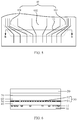
- the display area 01 of the display panel is an area surrounded by a dotted line shown in FIG. 2 , and an area outside the display area 01 is a non-display area 02.
- the "display area” mentioned herein refers to a pixel area capable of emitting light when the display panel is driven.
- the display panel of the display device shown in FIG. 2 includes a plurality of signal lines in the display area and a plurality of signal leading lines in the non-display area. The signal leading lines are electrically connected to the signal lines.
- FIG. 2 is a plan view of the display device, and the signal lines and the signal leading lines are not shown.
- FIG. 3 is a partial cross-sectional view taken along line A-A in FIG. 2 .
- the display device includes a display panel 10, and the signal leading lines 11 are also shown schematically in FIG. 3 .
- the display device further includes a light shielding pattern 30, which is located on the light-exit side of the display panel. An orthographic projection of the light shielding pattern 30 on the display panel is located within the non-display area 02.
- the light shielding pattern 30 is configured to block light reflected by the signal leading lines 11 from exiting out from the light-exit side.
- the light shielding pattern in the display device is provided for the signal leading lines of the display panel, and it is arranged in the non-display area of the display panel without affecting a normal display of the display device.
- the light shielding pattern merely blocks the light reflected by the signal leading lines from exiting out from the light-exit side of the display panel. Therefore, the intensity of the light reflected by the non-display area of the display panel (including the "fanout area” mentioned above) and perceived by the user may be at least significantly reduced, thereby at least alleviating the aforementioned "light leakage" phenomenon.
- the above-mentioned signal lines may be data lines, in this case, the above-mentioned signal leading lines may include data leading lines.
- the example of the display device in FIG. 3 also schematically illustrates a border pattern 21 of the display device.
- the border pattern is located on the light-exit side of the display panel 10.
- An orthographic projection of the border pattern 21 on the display panel 10 is located within the non-display area 02, and the orthographic projection of the light shielding pattern 30 on the display panel 10 at least partially overlaps with the orthographic projection of the border pattern 20 on the display panel 10.
- the expression "at least partially overlap” used herein may mean that the orthographic projection of the light shielding pattern 30 on the display panel 10 falls within the orthographic projection of the border pattern 20 on the display panel 10, or the orthographic projection of the border pattern 20 on the display panel 10 falls within the orthographic projection of the light shielding pattern 30 on the display panel 10, or there is an overlapped portion between the orthographic projection of the light shielding pattern 30 on the display panel and the orthographic projection of the border pattern 20 on the display panel 10.
- a vertical distance from the light shielding pattern 30 to the display panel 10 is smaller than a vertical distance from the border pattern 21 to the display panel 10.
- the border pattern 21 is formed on a cover plate 20 located above the display panel 10.
- the non-display area 02 of the display panel includes an edge non-display area 04 and a middle non-display area 05.
- the edge non-display area 04 refers to an area of the non-display area corresponding to the above border pattern.
- the middle non-display area 05 is an area other than the edge non-display area 04 in the non-display area.
- the middle non-display area 05 does not include the border pattern. That is to say, in the example of FIG. 2 , a window area surrounded by the border pattern of the display device (the area surrounded by an inner contour line of the dark-filled area) is larger than the display area 01 of the display device. In this way, a phenomenon that the border pattern shields the display area of the display device, which is caused by a bonding misalignment or insufficient process capability, may be avoided.
- At least a part of the orthographic projection of the light shielding pattern 30 on the display panel is located within a middle area between the display area of the display panel and the orthographic projection of the border pattern on the display panel. That is, for the example of FIG. 3 , a part of the orthographic projection of the light shielding pattern 30 on the display panel 10 is located within the middle non-display area 05.
- the orthographic projection of the light shielding pattern 30 on the display panel 10 falls within an orthographic projection of the middle non-display area 05 on the display panel 10, or the orthographic projection of the middle non-display area 05 on the display panel 10 falls within the orthographic projection of the light shielding pattern 30 on the display panel 10, or there is an overlapped portion between the orthographic projection of the light shielding pattern 30 on the display panel 10 and the orthographic projection of the middle non-display area 05 on the display panel 10.
- the orthographic projection of the light shielding pattern 30 on the display panel 10 overlaps with both an orthographic projection of the edge non-display area 04 on the display panel 10 and the orthographic projection of the middle non-display area 05 on the display panel 10.
- the orthographic projection of the light shielding pattern 30 on the display panel 10 coincides with the orthographic projection of the non-display area 02 on the display panel 10, or a part of the orthographic projection of the light shielding pattern 30 on the display panel 10 falls within the orthographic projection of the edge non-display area 04 on the display panel 10, and the other part of the orthographic projection of the light shielding pattern 30 on the display panel 10 falls within the orthographic projection of the middle non-display area 05 on the display panel 10.
- the display device shown in FIG. 3 is an example of a self-luminous display device, for example, an OLED display device.
- FIG. 3 also schematically illustrates a cover plate 20, a packaging layer 40, a polarizer 50, a touch electrode layer 60, and an optical adhesive layer 70.
- the packaging layer 40 may include a packaging cover plate or a packaging film.
- the arrangement of the light shielding pattern proposed in the present disclosure is not limited thereto, and the light shielding pattern may be arranged only in a single layer structure, or may be arranged on multiple layer structures, which will be further described below.
- FIG. 4 also schematically illustrates an optical path of light reflected by signal leading lines.
- the signal leading lines 11 located in the non-display area 02 reflect external ambient light or light emitted from the display device, most of the light may directly exit out of a display surface of the display device, and then is perceived by the user, as indicated by the optical path of the light reflected by the signal leading lines 11 on the left side in FIG. 3 .
- the user may still perceive a part of the light reflected by the signal leading lines 11 in the edge non-display area 04, as indicated by the optical path of the light reflected by the signal leading lines 11 on the right side in FIG. 3 . Therefore, for the example of FIG. 4 , the light reflected by the signal leading lines 11 located in the non-display area 02 may be perceived by the user, and the above-mentioned "light leakage" phenomenon is likely to occur, which affects the user 's experience of the display device adversely.
- FIG. 3 schematically illustrates an optical path of the light reflected by the signal leading lines 11 in the display device provided by some embodiments of the present disclosure.
- the display panel 10 includes a display area 01 and a non-display area 02.
- the non-display area 02 includes an edge non-display area 04 and a middle non-display area 05.
- the middle non-display area 05 is located between the display area 01 and the edge non-display area 04, and the fanout area 03 of the display panel is located in the non-display area 02. It may be well understood from FIG. 3 that after the light reflected by the signal leading lines 11 passes through the light shielding pattern 30, the intensity thereof is significantly reduced.
- the light shielding pattern 30 may at least reduce the intensity of the light reflected by the signal leading lines 11. In this way, the user's sensitivity to the light reflected by the signal leading lines 11 may be reduced, and the aforementioned "light leakage" phenomenon may be alleviated.
- the embodiments of the present disclosure do not specifically limit the layer structures on which the light shielding pattern is disposed.
- the light shielding pattern 30 may be disposed on any one or more layer structures selected from the packaging layer 40, the polarizer 50, the touch electrode layer 60, the optical solid-state adhesive layer 70 and so on.
- the light shielding pattern may be attached to a single layer structure of the display device.
- the light shielding pattern may be disposed only on the touch electrode layer 60.
- the material forming the light shielding pattern 30 includes, but is not limited to, ink.
- the light transmittance of the light shielding pattern 30 may be adjusted by adjusting factors such as the material of the light shielding pattern 30 and the thickness of the light shielding pattern, so that the light shielding pattern may block the light reflected by the signal leading lines to different degrees.
- FIG. 3 schematically illustrates the optical paths of the light reflected by different signal leading lines 11, FIG. 3 does not represent all the optical paths of the light reflected by the signal leading lines 11.
- reflected light from the middle non-display area 05 may include the light reflected by the signal leading lines located in the edge non-display area 04, or may also include the light reflected by the signal leading lines located in the middle non-display area 05.
- the reflection here may be mirror reflection or diffuse reflection.
- various portions of the light shielding pattern may have inconsistent light transmittances.
- an area in which the plurality of signal leading lines are located includes a first leading line area and a second leading line area.
- a light reflection capability of the first leading line area is higher than a light reflection capability of the second leading line area.
- the light shielding pattern includes a first pattern for blocking reflected light from the first leading line area and a second pattern for blocking reflected light from the second leading line area, and a light transmittance of the first pattern is lower than a light transmittance of the second pattern. That is to say, in this embodiment, the light shielding patterns 30 has different light transmittances in different areas so as to block or absorb the light reflected by the signal leading lines to different degrees.
- FIG. 5 schematically illustrates an example of "fanout area 03" and signal leading lines (for example, data leading lines) in the fanout area according to some embodiments of the present disclosure.
- the fanout area 03 includes a first fanout sub-area 031 and a second fanout sub-area 032.
- the light reflection capability of the signal leading lines 11 in the first fanout sub-area 031 is higher than the light reflection capability of the signal leading lines 11 in the second fanout sub-area 032. Therefore, in this example, the first fanout sub-area 031 may correspond to the first leading line area in the above embodiment and the second fanout sub-area 032 may correspond to the second leading line area in the above embodiment.
- the light shielding pattern includes a first pattern and a second pattern.
- the first pattern and the second pattern are used to block reflected light from different signal leading line areas, respectively, and the light transmittance of the first pattern is lower than that of the second pattern. In this way, the reflected light from the first leading line area with higher light reflection capability may be blocked by the first pattern to a higher degree, while the reflected light from the second leading line area may be blocked by the second pattern to a relatively low degree.
- first fanout sub-area 031 the first fanout sub-area 031
- second fanout sub-area 032 the second fanout sub-area 032
- a relative positional relationship between the first fanout sub-area 031 and the second fanout area 032 is not limited herein.
- the positional relationship between the first fanout sub-area 031 and the second fanout area 032 shown in FIG. 5 is only an example.
- the first fanout sub-area 031 may include multiple independent areas
- the second fanout sub-area 032 may also include multiple independent areas.
- the signal leading lines in the first fanout sub-area 031 and an anode of the organic light-emitting device of the self-luminous display panel are formed of the same material and formed through the same patterning process. That is, the signal leading lines 11 in the first fanout sub-area 031 and the anode of the organic light-emitting device are formed through the same patterning process (using the same mask).
- the material forming the anode may include, for example, ITO (Indium Tin Oxide), Ag (silver), or the like.
- the light reflection capability of the signal leading line is mainly related to characteristics of its material.
- the light reflection capability of the signal leading lines 11 in the fanout area is also related to the distribution density of the signal leading lines 11.
- the distribution density of the signal leading lines in the first leading line area is greater than the distribution density of the signal leading lines in the second leading line area.
- the distribution density of the signal leading lines 11 in the first fanout sub-area 031 is greater than the distribution density of the signal leading lines 11 in the second fanout sub-area 032. Therefore, the intensity of the reflected light in the first fanout sub-area 031 may be higher than the intensity of the reflected light in the second fanout sub-area 032.
- the reflectance of the material of the signal leading line 11 in the first fanout sub-area 031 is different from that of the material of the signal leading line 11 in the second fanout sub-area 031, which may also result in different light reflection capabilities in different leading line areas.
- FIG. 6 is a partial cross-sectional view of FIG. 5 taken along a line B-B in FIG. 5 .
- the light shielding pattern 30 includes a first pattern 31 corresponding to the first fanout sub-area 031 and a second pattern 32 corresponding to the second fanout sub-area 032.
- the light transmittance of the first pattern 31 is lower than the light transmittance of the second pattern 32.
- the light reflection capability of the signal leading lines 11 in the first fanout sub-area 031 is higher than that of the signal leading lines in the second fanout sub-area 032, and the light reflection capability of the signal leading lines in the second fanout sub-area 032 is higher than the light reflection capability of the signal leading lines in the other area of the non-display area 02 except the fanout area 03.
- the first pattern with a lower light transmittance blocks the first reflected light from the first fanout sub-area 031, so that the intensity of the first reflected light is greatly reduced.
- the second pattern with a relatively high light transmittance blocks the second reflected light from the second fanout sub-area 032, so that the intensity of the second reflected light is reduced to a small degree. In this way, the difference between the intensities of the light reflected by the signal leading lines in different areas may be reduced, which is beneficial to improving the comfort of the user when using the display device.
- the light shielding pattern includes a hollow pattern, and a proportion of the hollow portion of the first pattern 31 is smaller than a proportion of the hollow portion of the second pattern 32.
- the light shielding pattern includes a plurality of strips, and a density of the strips of the first pattern is greater than a density of the strips of the second pattern. In this way, it is possible to realize that the first pattern and the second pattern have different light transmittances.
- the specific shape of the hollow pattern is not limited. In the case where the light shielding pattern includes a plurality of hollow patterns, the shapes of the hollow patterns may not be completely the same.
- a plurality of small holes may be provided in the light shielding pattern 30, and the light transmittance of the light shielding pattern 30 may be adjusted by adjusting parameters such as a distribution density and sizes of the small holes.
- the light transmittance of the light shielding pattern 30 may be adjusted by adjusting a space between the strips.
- the light shielding pattern may be formed by coating ink on some layer structures above the display panel.
- a width of the light shielding pattern in a direction perpendicular to an edge of the display area closest to the light shielding pattern ranges from 0.5mm to 1mm.
- the width of the light shielding pattern 30 shown in FIG. 3 may range from 0.5mm to 1mm.
- the light shielding pattern may be arranged on a plurality of different layer structures above the display panel.
- sizes of the light shielding patterns on different layer structures may be different.
- the sizes of the light shielding pattern may be determined according to a distance between the light shielding pattern and the signal leading lines, so that the light shielding pattern blocks the light reflected by the signal leading lines from exiting out from the light-exit side, or different light shielding patterns block the reflected light from different leading line areas to different degrees.
- the light shielding pattern 30 may be disposed on a side of the layer structure distal to the display panel, or may be disposed on a side of the layer structure adjacent to the display panel.
- the display device herein may specifically include an OLED display, a television, a digital photo frame, a mobile phone, a tablet computer, a navigator, or any other product or component with any display function.
Landscapes
- Physics & Mathematics (AREA)
- Nonlinear Science (AREA)
- Optics & Photonics (AREA)
- Mathematical Physics (AREA)
- Chemical & Material Sciences (AREA)
- Crystallography & Structural Chemistry (AREA)
- General Physics & Mathematics (AREA)
- Engineering & Computer Science (AREA)
- Microelectronics & Electronic Packaging (AREA)
- Devices For Indicating Variable Information By Combining Individual Elements (AREA)
- Electroluminescent Light Sources (AREA)
- Liquid Crystal (AREA)
Applications Claiming Priority (2)
| Application Number | Priority Date | Filing Date | Title |
|---|---|---|---|
| CN201810872952.0A CN110794610B (zh) | 2018-08-02 | 2018-08-02 | 一种显示组件、显示装置 |
| PCT/CN2019/098791 WO2020025011A1 (fr) | 2018-08-02 | 2019-08-01 | Appareil d'affichage |
Publications (3)
| Publication Number | Publication Date |
|---|---|
| EP3832383A1 true EP3832383A1 (fr) | 2021-06-09 |
| EP3832383A4 EP3832383A4 (fr) | 2022-03-09 |
| EP3832383B1 EP3832383B1 (fr) | 2025-10-01 |
Family
ID=69231449
Family Applications (1)
| Application Number | Title | Priority Date | Filing Date |
|---|---|---|---|
| EP19832826.2A Active EP3832383B1 (fr) | 2018-08-02 | 2019-08-01 | Appareil d'affichage |
Country Status (10)
| Country | Link |
|---|---|
| US (1) | US11527598B2 (fr) |
| EP (1) | EP3832383B1 (fr) |
| JP (1) | JP7420736B2 (fr) |
| KR (1) | KR102492632B1 (fr) |
| CN (1) | CN110794610B (fr) |
| AU (1) | AU2019314744B2 (fr) |
| BR (1) | BR112020022577A2 (fr) |
| MX (1) | MX2020012296A (fr) |
| RU (1) | RU2756787C1 (fr) |
| WO (1) | WO2020025011A1 (fr) |
Families Citing this family (11)
| Publication number | Priority date | Publication date | Assignee | Title |
|---|---|---|---|---|
| CN111863919B (zh) * | 2020-07-29 | 2022-07-26 | 武汉天马微电子有限公司 | 显示面板和显示装置 |
| CN111916488A (zh) * | 2020-09-11 | 2020-11-10 | 京东方科技集团股份有限公司 | 一种显示基板、显示装置 |
| KR20230102339A (ko) * | 2021-12-30 | 2023-07-07 | 엘지디스플레이 주식회사 | 표시 장치 |
| CN114628615A (zh) * | 2022-03-31 | 2022-06-14 | 绵阳京东方光电科技有限公司 | 显示面板及其制备方法、显示模组及显示装置 |
| CN114823825B (zh) * | 2022-04-12 | 2025-01-28 | 武汉华星光电半导体显示技术有限公司 | 显示面板及显示装置 |
| EP4510812A1 (fr) | 2022-04-12 | 2025-02-19 | Wuhan China Star Optoelectronics Semiconductor Display Technology Co., Ltd. | Écran d'affichage et dispositif d'affichage |
| CN115101559B (zh) * | 2022-06-23 | 2025-09-19 | 武汉天马微电子有限公司 | 显示面板和显示装置 |
| CN115224090B (zh) * | 2022-06-29 | 2025-12-09 | 合肥维信诺科技有限公司 | 显示面板 |
| CN115568252B (zh) * | 2022-09-29 | 2025-04-01 | 京东方科技集团股份有限公司 | 显示基板、显示面板和显示装置 |
| CN118475871A (zh) * | 2022-11-29 | 2024-08-09 | 京东方科技集团股份有限公司 | 阵列基板和显示装置 |
| EP4648591A1 (fr) * | 2023-09-28 | 2025-11-12 | Boe Technology Group Co., Ltd. | Écran d'affichage et dispositif d'affichage |
Family Cites Families (34)
| Publication number | Priority date | Publication date | Assignee | Title |
|---|---|---|---|---|
| JP3669351B2 (ja) * | 2001-10-04 | 2005-07-06 | セイコーエプソン株式会社 | 電気光学装置及び電子機器 |
| KR100814339B1 (ko) * | 2001-11-16 | 2008-03-18 | 엘지.필립스 엘시디 주식회사 | 콜레스테릭 액정 컬러필터를 가지는 반사형 액정표시장치 |
| JP2005062619A (ja) * | 2003-08-18 | 2005-03-10 | Sony Corp | 液晶表示素子及びその製造方法並びに液晶表示装置 |
| JP4285158B2 (ja) * | 2003-08-29 | 2009-06-24 | セイコーエプソン株式会社 | 電気光学装置及び電子機器 |
| TWI265348B (en) * | 2003-09-24 | 2006-11-01 | Chunghwa Picture Tubes Ltd | Liquid crystal display device and the fabricating method thereof |
| TWI257516B (en) * | 2004-07-01 | 2006-07-01 | Hannstar Display Corp | ODF cell structure |
| JP5147462B2 (ja) * | 2007-03-06 | 2013-02-20 | 日東電工株式会社 | 反射遮光性構造および液晶表示装置 |
| JP5120066B2 (ja) * | 2007-08-02 | 2013-01-16 | セイコーエプソン株式会社 | 電気光学装置及び電子機器 |
| JP5536986B2 (ja) * | 2008-04-30 | 2014-07-02 | 三菱電機株式会社 | 液晶表示装置 |
| KR101002663B1 (ko) * | 2008-12-11 | 2010-12-21 | 삼성모바일디스플레이주식회사 | 유기 발광 표시 장치 |
| KR101765101B1 (ko) * | 2010-12-14 | 2017-08-07 | 엘지디스플레이 주식회사 | 액정표시장치 |
| TW201319661A (zh) * | 2011-11-02 | 2013-05-16 | Wintek Corp | 液晶顯示裝置 |
| US8755010B2 (en) * | 2011-11-17 | 2014-06-17 | Apple Inc. | Displays with multilayer masks and color filters |
| CN103123548B (zh) * | 2011-11-18 | 2016-12-07 | 宸鸿科技(厦门)有限公司 | 触控显示装置 |
| KR102022697B1 (ko) * | 2012-10-08 | 2019-09-19 | 삼성디스플레이 주식회사 | 표시 장치 |
| JP2014228673A (ja) * | 2013-05-22 | 2014-12-08 | セイコーエプソン株式会社 | 液晶装置、液晶装置の製造方法、及び電子機器 |
| KR102264472B1 (ko) * | 2013-07-01 | 2021-06-14 | 엘지디스플레이 주식회사 | 디스플레이 장치 |
| KR102338749B1 (ko) * | 2014-05-07 | 2021-12-15 | 삼성디스플레이 주식회사 | 표시 장치 |
| KR102238994B1 (ko) * | 2014-07-17 | 2021-04-12 | 엘지디스플레이 주식회사 | 표시장치 |
| KR20160094544A (ko) * | 2015-01-30 | 2016-08-10 | 엘지디스플레이 주식회사 | 디스플레이 장치 |
| US20160338188A1 (en) * | 2015-05-15 | 2016-11-17 | Microsoft Technology Licensing, Llc | Computing device bonding assemblies |
| KR102341639B1 (ko) | 2015-08-21 | 2021-12-21 | 삼성디스플레이 주식회사 | 액정 표시 장치 및 그의 제조 방법 |
| CN105204692B (zh) * | 2015-10-28 | 2018-01-26 | 京东方科技集团股份有限公司 | 一种触摸屏、显示装置及显示装置的显示驱动方法 |
| CN105739166B (zh) * | 2016-04-20 | 2020-02-21 | 昆山龙腾光电股份有限公司 | 液晶显示模组及液晶显示装置 |
| CN106057830A (zh) * | 2016-08-19 | 2016-10-26 | 京东方科技集团股份有限公司 | 一种阵列基板、显示面板及阵列基板制备方法 |
| WO2018100466A1 (fr) * | 2016-11-30 | 2018-06-07 | Semiconductor Energy Laboratory Co., Ltd. | Dispositif d'affichage, module d'affichage et dispositif électronique |
| CN106646995A (zh) * | 2016-12-21 | 2017-05-10 | 深圳市华星光电技术有限公司 | 一种避免漏光的液晶盒及液晶显示装置 |
| CN106483706A (zh) * | 2016-12-29 | 2017-03-08 | 惠科股份有限公司 | 液晶显示面板 |
| CN106681042B (zh) | 2017-01-05 | 2021-01-26 | 京东方科技集团股份有限公司 | 触控显示屏及其制造方法、触控显示装置 |
| CN107179642A (zh) * | 2017-07-04 | 2017-09-19 | 深圳市华星光电技术有限公司 | 液晶显示面板及液晶显示模组 |
| KR101995817B1 (ko) * | 2017-07-18 | 2019-07-03 | 주식회사 하이딥 | 터치 입력 장치 제조 방법 및 터치 입력 장치 |
| CN107247360B (zh) * | 2017-08-09 | 2020-06-23 | 深圳市华星光电技术有限公司 | 无边框液晶面板及其制作方法与显示装置 |
| CN108153071B (zh) * | 2017-12-29 | 2020-12-11 | 惠州市华星光电技术有限公司 | 显示面板及其制造方法、显示装置 |
| CN108807476B (zh) * | 2018-06-07 | 2020-12-22 | 武汉华星光电半导体显示技术有限公司 | 显示器面板 |
-
2018
- 2018-08-02 CN CN201810872952.0A patent/CN110794610B/zh active Active
-
2019
- 2019-08-01 RU RU2020137117A patent/RU2756787C1/ru active
- 2019-08-01 MX MX2020012296A patent/MX2020012296A/es unknown
- 2019-08-01 AU AU2019314744A patent/AU2019314744B2/en active Active
- 2019-08-01 KR KR1020207036308A patent/KR102492632B1/ko active Active
- 2019-08-01 JP JP2020558590A patent/JP7420736B2/ja active Active
- 2019-08-01 EP EP19832826.2A patent/EP3832383B1/fr active Active
- 2019-08-01 US US16/624,285 patent/US11527598B2/en active Active
- 2019-08-01 WO PCT/CN2019/098791 patent/WO2020025011A1/fr not_active Ceased
- 2019-08-01 BR BR112020022577-0A patent/BR112020022577A2/pt active IP Right Grant
Also Published As
| Publication number | Publication date |
|---|---|
| CN110794610A (zh) | 2020-02-14 |
| KR102492632B1 (ko) | 2023-01-30 |
| CN110794610B (zh) | 2024-07-26 |
| EP3832383B1 (fr) | 2025-10-01 |
| EP3832383A4 (fr) | 2022-03-09 |
| KR20210008539A (ko) | 2021-01-22 |
| MX2020012296A (es) | 2021-01-29 |
| RU2756787C1 (ru) | 2021-10-05 |
| WO2020025011A1 (fr) | 2020-02-06 |
| BR112020022577A2 (pt) | 2021-02-17 |
| AU2019314744B2 (en) | 2021-11-18 |
| JP2021532433A (ja) | 2021-11-25 |
| AU2019314744A1 (en) | 2020-11-26 |
| JP7420736B2 (ja) | 2024-01-23 |
| US11527598B2 (en) | 2022-12-13 |
| US20210335983A1 (en) | 2021-10-28 |
Similar Documents
| Publication | Publication Date | Title |
|---|---|---|
| US11527598B2 (en) | Display device | |
| CN212873152U (zh) | 一种显示面板及显示装置 | |
| US11333914B2 (en) | Electro-optical device and electronic equipment | |
| CN109100892B (zh) | 一种液晶显示面板及显示装置 | |
| US8284330B2 (en) | Display apparatus having light-shielding layer and variable light-transmittance pattern | |
| CN109541833A (zh) | 显示组件、显示装置及其驱动方法 | |
| US8045068B2 (en) | Display apparatus with gradation pattern near display boundary | |
| KR20220098036A (ko) | 디스플레이 기판, 디스플레이 패널 및 디스플레이 장치 | |
| US20200133082A1 (en) | Liquid crystal display panel and manufacturing method thereof | |
| KR102460231B1 (ko) | 백라이트 유닛 및 이를 포함하는 액정 표시 장치 | |
| CN110955084A (zh) | 一种显示装置及其驱动方法 | |
| CN102067587A (zh) | 显示装置 | |
| US20210335919A1 (en) | Display panel and terminal device thereof | |
| CN113630486A (zh) | 电子设备及显示屏 | |
| US20180348925A1 (en) | Touch substrate, touch screen and its manufacturing method, and display device | |
| US12426485B2 (en) | Display panel and display device | |
| CN113013219A (zh) | 显示装置 | |
| TWI499838B (zh) | 顯示裝置 | |
| CN115327807A (zh) | 显示面板、显示模组和显示装置 | |
| KR20100112413A (ko) | 디스플레이 장치 | |
| KR20100112410A (ko) | 디스플레이 장치 | |
| KR20220094879A (ko) | 표시 장치 | |
| KR20100112411A (ko) | 디스플레이 장치 | |
| KR20100112412A (ko) | 디스플레이 장치 | |
| KR20110086242A (ko) | 디스플레이 장치 |
Legal Events
| Date | Code | Title | Description |
|---|---|---|---|
| STAA | Information on the status of an ep patent application or granted ep patent |
Free format text: STATUS: UNKNOWN |
|
| STAA | Information on the status of an ep patent application or granted ep patent |
Free format text: STATUS: THE INTERNATIONAL PUBLICATION HAS BEEN MADE |
|
| PUAI | Public reference made under article 153(3) epc to a published international application that has entered the european phase |
Free format text: ORIGINAL CODE: 0009012 |
|
| STAA | Information on the status of an ep patent application or granted ep patent |
Free format text: STATUS: REQUEST FOR EXAMINATION WAS MADE |
|
| 17P | Request for examination filed |
Effective date: 20200117 |
|
| AK | Designated contracting states |
Kind code of ref document: A1 Designated state(s): AL AT BE BG CH CY CZ DE DK EE ES FI FR GB GR HR HU IE IS IT LI LT LU LV MC MK MT NL NO PL PT RO RS SE SI SK SM TR |
|
| DAV | Request for validation of the european patent (deleted) | ||
| DAX | Request for extension of the european patent (deleted) | ||
| A4 | Supplementary search report drawn up and despatched |
Effective date: 20220209 |
|
| RIC1 | Information provided on ipc code assigned before grant |
Ipc: H01L 51/52 20060101ALN20220203BHEP Ipc: H01L 27/32 20060101ALN20220203BHEP Ipc: G02F 1/1345 20060101ALI20220203BHEP Ipc: G02F 1/1335 20060101ALI20220203BHEP Ipc: G02F 1/1333 20060101AFI20220203BHEP |
|
| REG | Reference to a national code |
Ref legal event code: R079 Ipc: G02F0001133300 Ref country code: DE Ref legal event code: R079 Ref document number: 602019076439 Country of ref document: DE Free format text: PREVIOUS MAIN CLASS: G02F0001133500 Ipc: G02F0001133300 |
|
| GRAP | Despatch of communication of intention to grant a patent |
Free format text: ORIGINAL CODE: EPIDOSNIGR1 |
|
| STAA | Information on the status of an ep patent application or granted ep patent |
Free format text: STATUS: GRANT OF PATENT IS INTENDED |
|
| RIC1 | Information provided on ipc code assigned before grant |
Ipc: H10K 59/80 20230101ALN20250602BHEP Ipc: H10K 59/131 20230101ALN20250602BHEP Ipc: H10K 59/126 20230101ALN20250602BHEP Ipc: G02F 1/1345 20060101ALI20250602BHEP Ipc: G02F 1/1335 20060101ALI20250602BHEP Ipc: G02F 1/1333 20060101AFI20250602BHEP |
|
| INTG | Intention to grant announced |
Effective date: 20250612 |
|
| GRAS | Grant fee paid |
Free format text: ORIGINAL CODE: EPIDOSNIGR3 |
|
| GRAA | (expected) grant |
Free format text: ORIGINAL CODE: 0009210 |
|
| STAA | Information on the status of an ep patent application or granted ep patent |
Free format text: STATUS: THE PATENT HAS BEEN GRANTED |
|
| AK | Designated contracting states |
Kind code of ref document: B1 Designated state(s): AL AT BE BG CH CY CZ DE DK EE ES FI FR GB GR HR HU IE IS IT LI LT LU LV MC MK MT NL NO PL PT RO RS SE SI SK SM TR |
|
| REG | Reference to a national code |
Ref country code: GB Ref legal event code: FG4D Ref country code: CH Ref legal event code: F10 Free format text: ST27 STATUS EVENT CODE: U-0-0-F10-F00 (AS PROVIDED BY THE NATIONAL OFFICE) Effective date: 20251001 |
|
| REG | Reference to a national code |
Ref country code: DE Ref legal event code: R096 Ref document number: 602019076439 Country of ref document: DE |
|
| REG | Reference to a national code |
Ref country code: IE Ref legal event code: FG4D |
|
| REG | Reference to a national code |
Ref country code: NL Ref legal event code: MP Effective date: 20251001 |
|
| REG | Reference to a national code |
Ref country code: AT Ref legal event code: MK05 Ref document number: 1843078 Country of ref document: AT Kind code of ref document: T Effective date: 20251001 |
|
| PG25 | Lapsed in a contracting state [announced via postgrant information from national office to epo] |
Ref country code: NL Free format text: LAPSE BECAUSE OF FAILURE TO SUBMIT A TRANSLATION OF THE DESCRIPTION OR TO PAY THE FEE WITHIN THE PRESCRIBED TIME-LIMIT Effective date: 20251001 |
|
| PG25 | Lapsed in a contracting state [announced via postgrant information from national office to epo] |
Ref country code: ES Free format text: LAPSE BECAUSE OF FAILURE TO SUBMIT A TRANSLATION OF THE DESCRIPTION OR TO PAY THE FEE WITHIN THE PRESCRIBED TIME-LIMIT Effective date: 20251001 |
|
| REG | Reference to a national code |
Ref country code: LT Ref legal event code: MG9D |
|
| PG25 | Lapsed in a contracting state [announced via postgrant information from national office to epo] |
Ref country code: NO Free format text: LAPSE BECAUSE OF FAILURE TO SUBMIT A TRANSLATION OF THE DESCRIPTION OR TO PAY THE FEE WITHIN THE PRESCRIBED TIME-LIMIT Effective date: 20260101 |
|
| PG25 | Lapsed in a contracting state [announced via postgrant information from national office to epo] |
Ref country code: FI Free format text: LAPSE BECAUSE OF FAILURE TO SUBMIT A TRANSLATION OF THE DESCRIPTION OR TO PAY THE FEE WITHIN THE PRESCRIBED TIME-LIMIT Effective date: 20251001 Ref country code: AT Free format text: LAPSE BECAUSE OF FAILURE TO SUBMIT A TRANSLATION OF THE DESCRIPTION OR TO PAY THE FEE WITHIN THE PRESCRIBED TIME-LIMIT Effective date: 20251001 Ref country code: HR Free format text: LAPSE BECAUSE OF FAILURE TO SUBMIT A TRANSLATION OF THE DESCRIPTION OR TO PAY THE FEE WITHIN THE PRESCRIBED TIME-LIMIT Effective date: 20251001 |
|
| PG25 | Lapsed in a contracting state [announced via postgrant information from national office to epo] |
Ref country code: RS Free format text: LAPSE BECAUSE OF FAILURE TO SUBMIT A TRANSLATION OF THE DESCRIPTION OR TO PAY THE FEE WITHIN THE PRESCRIBED TIME-LIMIT Effective date: 20260101 |
|
| PG25 | Lapsed in a contracting state [announced via postgrant information from national office to epo] |
Ref country code: IS Free format text: LAPSE BECAUSE OF FAILURE TO SUBMIT A TRANSLATION OF THE DESCRIPTION OR TO PAY THE FEE WITHIN THE PRESCRIBED TIME-LIMIT Effective date: 20260201 |
|
| PG25 | Lapsed in a contracting state [announced via postgrant information from national office to epo] |
Ref country code: PT Free format text: LAPSE BECAUSE OF FAILURE TO SUBMIT A TRANSLATION OF THE DESCRIPTION OR TO PAY THE FEE WITHIN THE PRESCRIBED TIME-LIMIT Effective date: 20260202 Ref country code: CZ Free format text: LAPSE BECAUSE OF FAILURE TO SUBMIT A TRANSLATION OF THE DESCRIPTION OR TO PAY THE FEE WITHIN THE PRESCRIBED TIME-LIMIT Effective date: 20251001 |
|
| PG25 | Lapsed in a contracting state [announced via postgrant information from national office to epo] |
Ref country code: PL Free format text: LAPSE BECAUSE OF FAILURE TO SUBMIT A TRANSLATION OF THE DESCRIPTION OR TO PAY THE FEE WITHIN THE PRESCRIBED TIME-LIMIT Effective date: 20251001 |
|
| PG25 | Lapsed in a contracting state [announced via postgrant information from national office to epo] |
Ref country code: LV Free format text: LAPSE BECAUSE OF FAILURE TO SUBMIT A TRANSLATION OF THE DESCRIPTION OR TO PAY THE FEE WITHIN THE PRESCRIBED TIME-LIMIT Effective date: 20251001 |