EP3832499A1 - Dispositif de calcul de matrice - Google Patents
Dispositif de calcul de matrice Download PDFInfo
- Publication number
- EP3832499A1 EP3832499A1 EP21154586.8A EP21154586A EP3832499A1 EP 3832499 A1 EP3832499 A1 EP 3832499A1 EP 21154586 A EP21154586 A EP 21154586A EP 3832499 A1 EP3832499 A1 EP 3832499A1
- Authority
- EP
- European Patent Office
- Prior art keywords
- matrix
- instruction
- storage unit
- matrix operation
- operation instruction
- Prior art date
- Legal status (The legal status is an assumption and is not a legal conclusion. Google has not performed a legal analysis and makes no representation as to the accuracy of the status listed.)
- Granted
Links
Images




Classifications
-
- G—PHYSICS
- G06—COMPUTING OR CALCULATING; COUNTING
- G06F—ELECTRIC DIGITAL DATA PROCESSING
- G06F17/00—Digital computing or data processing equipment or methods, specially adapted for specific functions
- G06F17/10—Complex mathematical operations
- G06F17/16—Matrix or vector computation, e.g. matrix-matrix or matrix-vector multiplication, matrix factorization
Definitions
- the present disclosure relates to a matrix computing device for executing a matrix operation according to a matrix operation instruction, offering a solution to the problem in the prior art where more and more algorithms involve a large number of matrix operations.
- a plurality of neural network algorithms contain numerous matrix operations.
- the matrix operation has become an important issue to be considered at the beginning of designing various computing devices.
- one solution to conduct a matrix operation is to use a general-purpose processor, wherein a general-purpose instruction is executed by using a general-purpose register file and a general-purpose functional unit to perform a matrix operation.
- the solution may have the following disadvantages: the operation performance may be low during a matrix operation because a single general-purpose processor is primarily used for a scalar computation, while intercommunication among multiple processors may be a possible performance bottleneck when multiple general-purpose processors are used for parallel operations.
- a graphics processing unit (GPU) is used to perform a matrix computation, wherein a general-purpose SIMD instruction is executed by using a general-purpose register file and a general-purpose stream processing unit to perform a matrix operation.
- GPU graphics processing unit
- small on-chip cache of GPU requires constant transportation of off-chip data during a large-scale matrix operation, which makes off-chip bandwidth a main performance bottleneck.
- a specialized matrix operation device is used to perform a matrix computation, wherein a customized register file and a customized processing unit are used to perform a matrix operation.
- the current specialized matrix operation device is limited by the register file and is unable to flexibly support matrix operations of different lengths.
- the present disclosure aims to provide a matrix computing device to solve the problems existing in the prior art, such as constraints imposed by inter-chip communication, insufficient on-chip cache, and inflexible supported matrix length.
- the present disclosure provides a matrix computing device configured to execute a matrix operation according to a matrix operation instruction.
- the device includes:
- the matrix computing device provided by the present disclosure is able to temporarily store matrix data involved in computation in a scratchpad memory, supporting data of different widths in matrix operations more flexibly and effectively while improving the performance for executing computing tasks that contain a large number of matrices.
- the instruction adopted by the present disclosure has a simplified format, which makes the instruction set convenient to use and the supported matrix length more flexible.
- the present disclosure provides a matrix computing device including a storage unit, a register unit, and a matrix operation unit.
- the storage unit is configured to store matrices.
- the register unit is configured to store matrix storage addresses.
- the matrix operation unit is configured to acquire a matrix address from the register unit according to a matrix operation instruction, and then acquire a corresponding matrix from the storage unit according to the matrix address, subsequently perform a matrix operation according to the matrix acquired so as to obtain a matrix operation result.
- the matrix computing device provided by the present disclosure is able to temporarily store matrix data involved in computation in a scratchpad memory, supporting data of different widths in matrix operations more flexibly and effectively while improving the performance for executing computing tasks that contain a large number of matrices.
- Fig. 1 is a structure diagram of a matrix computing device provided by the present disclosure. As shown in Fig. 1 , the matrix computing device includes the following units:
- the matrix computing device further includes an instruction cache unit configured to store a matrix operation instruction to be executed. While being executed, an instruction is cached in the instruction cache unit as well. When execution of an instruction has been completed, if such instruction is also the earliest one among those instructions in the instruction cache unit that have not been submitted, then it will be submitted; once such instruction is submitted, the status change of the device caused by operation performed by such instruction cannot be cancelled.
- the instruction cache unit can be a reorder cache.
- the matrix computing device further includes an instruction processing unit configured to acquire a matrix operation instruction from the instruction cache unit and process the matrix operation instruction and provide the same to said matrix operation unit.
- the instruction processing unit includes:
- the matrix computing device further includes a dependency relationship processing unit configured to: before the matrix operation unit acquires the matrix operation instruction, determine whether the matrix operation instruction accesses the same matrix as the previous matrix operation instruction: if the matrix operation instruction does, the matrix operation instruction will be stored in a storage queue, and the matrix operation instruction in the storage queue will then be provided to said matrix operation unit the execution of the previous matrix operation instruction is completed; otherwise, the matrix operation instruction will be directly provided to said matrix operation unit.
- a dependency relationship processing unit configured to: before the matrix operation unit acquires the matrix operation instruction, determine whether the matrix operation instruction accesses the same matrix as the previous matrix operation instruction: if the matrix operation instruction does, the matrix operation instruction will be stored in a storage queue, and the matrix operation instruction in the storage queue will then be provided to said matrix operation unit the execution of the previous matrix operation instruction is completed; otherwise, the matrix operation instruction will be directly provided to said matrix operation unit.
- the matrix operation instruction accesses the scratchpad memory
- successive instructions may access the same memory space, and to ensure the correctness of an execution result of the instruction, the present instruction, if detected to have a dependency relationship with data of a previous instruction, must wait within the storage queue until such dependency relationship is eliminated.
- the matrix computing device further includes an in-out unit configured to store matrices in the storage unit or acquire a matrix operation result from the storage unit, wherein the in-out unit can directly connect with the storage unit and is configured to read or write matrix data from or in the memory.
- a structure of Load/Store is applied to the instruction set used for the present disclosure, and the matrix operation unit will not operate data in the internal storage.
- the instruction set adopts a simplified instruction set architecture and only provides the most basic vector fundamental-rule operations. Complex vector fundamental-rule operations are simulated by these simple instructions through combination thereof, making it possible to execute instructions in a single cycle at a high clock frequency.
- the instruction set also uses fixed-length instructions, so that the vector fundamental-rule operation device provided by the present disclosure fetches a next instruction in a decoding stage of a previous instruction.
- Fig.2 is a format diagram of the instruction set provided by the present disclosure.
- the matrix operation instruction includes an operation code and at least one operation field.
- the operation code is used for indicating the function of the matrix operation instruction, and the matrix operation unit is to perform different matrix operations by identifying the operation code; and the operation field is used for indicating data information of the matrix operation instruction, where the data information can be an immediate operand or a register number.
- matrix starting address and matrix length can be obtained from the corresponding register according to a register number, and then the matrix stored in the corresponding address can be obtained from the storage unit according to the matrix starting address and matrix length.
- the instruction set includes matrix operation instructions different in functions.
- MMV Matrix Multiplying Vector Instruction
- the device fetches matrix data and vector data with specified size from specified addresses of the scratchpad memory to perform multiplication between the matrix and the vector in the matrix operation unit, and writes the result back into a specified address of the scratchpad memory; it should be noted that a vector can be stored as a matrix of a specific form (with only one row of elements) in the scratchpad memory.
- VMM Vector Multiplying Matrix Instruction
- the device fetches vector data and matrix data with a specified size from specified addresses of the scratchpad memory to perform multiplication between the vector and the matrix in the matrix operation unit, and writes the result back into a specified address of the scratchpad memory; it should be noted that a vector can be stored as a matrix of a specific form (with only one row of elements) in the scratchpad memory.
- VMS Matrix Multiplying Scalar Instruction
- the device fetches matrix data of a specified size from a specified address of the scratchpad memory and scalar data of a specified size from a specified address of the scalar register file, multiplies scalar and matrix in the matrix operation unit and writes the result back into a specified address of the scratchpad memory.
- scalar register file stores both the matrix address and scalar data.
- the device respectively fetches two blocks of matrix data of a specified size from two specified addresses of the scratchpad memory, performs a tensor operation on the two matrix data in the matrix operation unit, and writes the result back into a specified address of the scratchpad memory;
- the device fetches two blocks of matrix data of two specified size from two specified addresses of the scratchpad memory, performs an addition operation on the two matrices in the matrix operation unit, and writes the result back into a specified address of the scratchpad memory;
- the device fetches two blocks of matrix data of a specified size respectively from two specified addresses of the scratchpad memory, performs a subtraction operation on the two matrices in the matrix operation unit, and writes the result back into a specified address of the scratchpad memory;
- the device fetches vector data of a specified size from a specified address of the scratchpad memory, and fetches matrix data of a specified size from a specified address of the scratchpad memory, where the vector in matrix operation unit is an index vector, and the i th element in an output vector is the number found in the i th column of the matrix by using the i th element of the index vector as an index, and the output vector is written back into a specified address of the scratchpad memory;
- the device loads data of a specified size from a specified external source address to a specified address of the scratchpad memory;
- the device stores matrix data of a specified size from a specified address of the scratchpad memory into an external destination address;
- MMOVE Matrix Movement Instruction
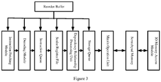
- Fig. 3 is a structure diagram of the matrix computing device provided by the embodiments of the present disclosure.
- the device includes an instruction fetching module, a decoding module, an instruction queue, a scalar register file, a dependency relationship processing unit, a storage queue, a reorder buffer, a matrix operation unit, a scratchpad memory, and an IO memory access module.
- the instruction fetching module is configured to obtain a next instruction to be executed from the instruction sequence and transmit the instruction to the decoding module.
- the decoding module is configured to decode the instruction and transmit the decoded instruction to the instruction queue.
- the instruction queue is configured to, considering the possible dependency relationship between different instructions on the scalar register, cache the decoded instruction and then send the instruction when the dependency relationship is satisfied.
- the scalar register file is configured to provide the device with scalar register as needed in operations.
- the dependency relationship processing unit is configured to process the possible storage dependency relationship between the instruction to be processed and a previous instruction of the instruction to be processed.
- the matrix operation instruction would access the scratchpad memory, and successive instructions may access the same memory space.
- the current instruction if detected to have a dependency relationship with data of the previous instruction, must wait within the storage queue until such dependency relationship is eliminated.
- the storage queue is a module with a sequential queue, where an instruction having a dependency relationship with the previous instruction in terms of data is stored in such queue until the dependency relationship is eliminated.
- the reorder buffer is a module where an instruction is cached while the instruction is being executed. When the execution of an instruction has been completed, if such instruction is also the earliest one among those instructions in the reorder buffer that have not been submitted, then it will be submitted; once such instruction is submitted, the status change of the device caused by execution of such instruction cannot be cancelled.
- the matrix operation unit is responsible for all the matrix operations of the device, including but not limited to matrix addition operation, matrix-add-scalar operation, matrix subtraction operation, matrix-subtract-scalar operation, matrix multiplication operation, matrix-multiply-scalar operation, matrix division (element-wise division) operation, matrix AND operation, and matrix OR operation, and the matrix operation instructions are sent to the operation unit for execution.
- the scratchpad memory is a temporary storage device specialized for matrix data, and capable to support matrix data of different sizes.
- An IO memory access module configured to directly access the scratchpad memory, and read or write data from or into the scratchpad memory.
- Fig. 4 is a flowchart illustrating a process that the matrix computing device provided by the embodiment of the present disclosure executes a matrix-multiply-vector instruction. As shown in Fig. 4 , the process of performing the matrix-multiply-vector instruction includes:
- Fig. 5 is a flowchart showing that the matrix computing device provided by the embodiments of the present disclosure performs a power multiplication to calculate an eigenvector corresponding to a maximum eigenvalue of an irreducible matrix. As illustrated in Fig. 5 , the process includes:
- Fig. 6 is a structure diagram of the matrix operation unit provided by the present disclosure.
- the matrix operation unit includes a matrix addition element, a matrix multiplication element, a matrix scalar multiplication element, and a nonlinear operation element.
- the matrix operation unit is in the structure of multiple-stage pipeline, where the matrix multiplication element and the matrix scalar multiplication element are arranged in pipeline stage 1, the matrix addition element in stage 2, and the nonlinear operation element in stage 3. Due to the fact that such elements are arranged in different stages of pipeline, when the order of a plurality of matrix operation instructions that are successive and serial is consistent with pipeline order of the corresponding units, the operations as demanded by the series of matrix operation instructions can be more effectively performed.
- the matrix computing device together with the reduced instruction set architecture offers a solution to the problem in the prior art that more and more algorithms involve a large number of matrix operations.
- the present disclosure features such technical effects as easy to use, supportive in various matrices and sufficient on-chip cache.
- the present disclosure is useful in many computing tasks involving numerous matrix operations, including the back training and forward prediction in the popular artificial neural network algorithm as well as the traditional numerical computation method of power multiplication for calculating a maximum eigenvalue of an irreducible matrix.
Landscapes
- Engineering & Computer Science (AREA)
- Physics & Mathematics (AREA)
- General Physics & Mathematics (AREA)
- Mathematical Physics (AREA)
- Pure & Applied Mathematics (AREA)
- Mathematical Analysis (AREA)
- Mathematical Optimization (AREA)
- Computational Mathematics (AREA)
- Data Mining & Analysis (AREA)
- Theoretical Computer Science (AREA)
- Computing Systems (AREA)
- Algebra (AREA)
- Databases & Information Systems (AREA)
- Software Systems (AREA)
- General Engineering & Computer Science (AREA)
- Advance Control (AREA)
- Complex Calculations (AREA)
Applications Claiming Priority (3)
| Application Number | Priority Date | Filing Date | Title |
|---|---|---|---|
| CN201610037535.5A CN106991077A (zh) | 2016-01-20 | 2016-01-20 | 一种矩阵计算装置 |
| EP16885911.4A EP3407202A4 (fr) | 2016-01-20 | 2016-04-06 | Appareil de calcul de matrice |
| PCT/CN2016/078546 WO2017124647A1 (fr) | 2016-01-20 | 2016-04-06 | Appareil de calcul de matrice |
Related Parent Applications (1)
| Application Number | Title | Priority Date | Filing Date |
|---|---|---|---|
| EP16885911.4A Division EP3407202A4 (fr) | 2016-01-20 | 2016-04-06 | Appareil de calcul de matrice |
Publications (3)
| Publication Number | Publication Date |
|---|---|
| EP3832499A1 true EP3832499A1 (fr) | 2021-06-09 |
| EP3832499C0 EP3832499C0 (fr) | 2023-07-12 |
| EP3832499B1 EP3832499B1 (fr) | 2023-07-12 |
Family
ID=59361386
Family Applications (2)
| Application Number | Title | Priority Date | Filing Date |
|---|---|---|---|
| EP21154586.8A Active EP3832499B1 (fr) | 2016-01-20 | 2016-04-06 | Dispositif de calcul de matrice |
| EP16885911.4A Ceased EP3407202A4 (fr) | 2016-01-20 | 2016-04-06 | Appareil de calcul de matrice |
Family Applications After (1)
| Application Number | Title | Priority Date | Filing Date |
|---|---|---|---|
| EP16885911.4A Ceased EP3407202A4 (fr) | 2016-01-20 | 2016-04-06 | Appareil de calcul de matrice |
Country Status (4)
| Country | Link |
|---|---|
| EP (2) | EP3832499B1 (fr) |
| KR (1) | KR102123633B1 (fr) |
| CN (2) | CN106991077A (fr) |
| WO (1) | WO2017124647A1 (fr) |
Families Citing this family (33)
| Publication number | Priority date | Publication date | Assignee | Title |
|---|---|---|---|---|
| CN107315718B (zh) * | 2016-04-26 | 2020-08-21 | 中科寒武纪科技股份有限公司 | 一种用于执行向量内积运算的装置和方法 |
| US20200110635A1 (en) | 2017-07-05 | 2020-04-09 | Shanghai Cambricon Information Technology Co., Ltd. | Data processing apparatus and method |
| CN109583577B (zh) * | 2017-09-29 | 2021-04-23 | 上海寒武纪信息科技有限公司 | 运算装置及方法 |
| EP3660629B1 (fr) | 2017-07-05 | 2023-08-30 | Shanghai Cambricon Information Technology Co., Ltd | Appareil et procédé de traitement de données |
| CN107578014B (zh) | 2017-09-06 | 2020-11-03 | 上海寒武纪信息科技有限公司 | 信息处理装置及方法 |
| CN107832843B (zh) * | 2017-10-30 | 2021-09-21 | 上海寒武纪信息科技有限公司 | 一种信息处理方法及相关产品 |
| CN109754062B (zh) * | 2017-11-07 | 2024-05-14 | 上海寒武纪信息科技有限公司 | 卷积扩展指令的执行方法以及相关产品 |
| CN108037908B (zh) * | 2017-12-15 | 2021-02-09 | 中科寒武纪科技股份有限公司 | 一种计算方法及相关产品 |
| CN108009126B (zh) * | 2017-12-15 | 2021-02-09 | 安徽寒武纪信息科技有限公司 | 一种计算方法及相关产品 |
| CN108108190B (zh) * | 2017-12-15 | 2020-01-24 | 中科寒武纪科技股份有限公司 | 一种计算方法及相关产品 |
| CN112230994B (zh) * | 2017-12-15 | 2024-12-27 | 安徽寒武纪信息科技有限公司 | 一种计算方法及相关产品 |
| CN108090028B (zh) * | 2017-12-15 | 2021-03-23 | 中科寒武纪科技股份有限公司 | 一种计算方法及相关产品 |
| CN108021393B (zh) * | 2017-12-15 | 2020-10-27 | 安徽寒武纪信息科技有限公司 | 一种计算方法及相关产品 |
| CN108121688B (zh) * | 2017-12-15 | 2020-06-23 | 中科寒武纪科技股份有限公司 | 一种计算方法及相关产品 |
| CN107957975B (zh) * | 2017-12-15 | 2021-01-05 | 安徽寒武纪信息科技有限公司 | 一种计算方法及相关产品 |
| CN107943756B (zh) * | 2017-12-15 | 2021-03-23 | 中科寒武纪科技股份有限公司 | 一种计算方法及相关产品 |
| CN107957976B (zh) * | 2017-12-15 | 2020-12-18 | 安徽寒武纪信息科技有限公司 | 一种计算方法及相关产品 |
| CN108388446A (zh) * | 2018-02-05 | 2018-08-10 | 上海寒武纪信息科技有限公司 | 运算模块以及方法 |
| CN108960418A (zh) * | 2018-08-08 | 2018-12-07 | 上海寒武纪信息科技有限公司 | 神经网络处理装置及其执行矩阵向量乘指令的方法 |
| US12094456B2 (en) | 2018-09-13 | 2024-09-17 | Shanghai Cambricon Information Technology Co., Ltd. | Information processing method and system |
| CN110941789B (zh) * | 2018-09-21 | 2023-12-15 | 北京地平线机器人技术研发有限公司 | 张量运算方法和装置 |
| CN110119807B (zh) * | 2018-10-12 | 2021-11-09 | 上海寒武纪信息科技有限公司 | 运算方法、装置、计算机设备和存储介质 |
| CN111290789B (zh) * | 2018-12-06 | 2022-05-27 | 上海寒武纪信息科技有限公司 | 运算方法、装置、计算机设备和存储介质 |
| CN111198670B (zh) | 2018-11-20 | 2021-01-29 | 华为技术有限公司 | 执行矩阵乘法运算的方法、电路及soc |
| CN111381871B (zh) * | 2018-12-28 | 2022-12-09 | 上海寒武纪信息科技有限公司 | 运算方法、装置及相关产品 |
| CN111966399B (zh) * | 2019-05-20 | 2024-06-07 | 上海寒武纪信息科技有限公司 | 指令处理方法、装置及相关产品 |
| CN112463215B (zh) * | 2019-09-09 | 2024-06-07 | 腾讯科技(深圳)有限公司 | 数据处理方法、装置、计算机可读存储介质和计算机设备 |
| CN113836481B (zh) * | 2020-06-24 | 2024-07-02 | 广州希姆半导体科技有限公司 | 矩阵计算电路、方法、电子设备及计算机可读存储介质 |
| CN113867799B (zh) * | 2020-06-30 | 2025-05-02 | 上海寒武纪信息科技有限公司 | 计算装置、集成电路芯片、板卡、电子设备和计算方法 |
| CN111930506A (zh) * | 2020-08-13 | 2020-11-13 | 山东云海国创云计算装备产业创新中心有限公司 | 一种矩阵调度方法及相关装置 |
| CN114168896B (zh) * | 2020-09-11 | 2025-09-09 | 广州希姆半导体科技有限公司 | 矩阵计算电路、方法、电子设备及计算机可读存储介质 |
| CN114168894B (zh) * | 2020-09-11 | 2025-07-08 | 广州希姆半导体科技有限公司 | 矩阵计算电路、方法、电子设备及计算机可读存储介质 |
| CN112328960B (zh) * | 2020-11-02 | 2023-09-19 | 中国平安财产保险股份有限公司 | 数据运算的优化方法、装置、电子设备及存储介质 |
Citations (2)
| Publication number | Priority date | Publication date | Assignee | Title |
|---|---|---|---|---|
| US4888679A (en) * | 1988-01-11 | 1989-12-19 | Digital Equipment Corporation | Method and apparatus using a cache and main memory for both vector processing and scalar processing by prefetching cache blocks including vector data elements |
| US6282634B1 (en) * | 1998-05-27 | 2001-08-28 | Arm Limited | Apparatus and method for processing data having a mixed vector/scalar register file |
Family Cites Families (13)
| Publication number | Priority date | Publication date | Assignee | Title |
|---|---|---|---|---|
| JPH04365170A (ja) * | 1991-06-12 | 1992-12-17 | Mitsubishi Electric Corp | ディジタル信号処理用半導体集積回路装置 |
| US5669013A (en) * | 1993-10-05 | 1997-09-16 | Fujitsu Limited | System for transferring M elements X times and transferring N elements one time for an array that is X*M+N long responsive to vector type instructions |
| JP2000259609A (ja) * | 1999-03-12 | 2000-09-22 | Hitachi Ltd | データ処理プロセッサおよびシステム |
| JP5157484B2 (ja) | 2008-01-30 | 2013-03-06 | ヤマハ株式会社 | 行列演算コプロセッサ |
| CN101620524B (zh) * | 2009-07-03 | 2011-08-10 | 中国人民解放军国防科学技术大学 | 支持矩阵整体读写操作的矩阵寄存器文件 |
| WO2012037472A2 (fr) * | 2010-09-17 | 2012-03-22 | William Marsh Rice University | Calculateur rapide de dose avec gpu utilisé dans le traitement du cancer |
| CN102360344B (zh) * | 2011-10-10 | 2014-03-12 | 西安交通大学 | 矩阵处理器及其指令集和嵌入式系统 |
| WO2013054468A1 (fr) * | 2011-10-14 | 2013-04-18 | パナソニック株式会社 | Appareil d'opération de transposition, son circuit intégré et procédé de traitement de transposition |
| CN102521535A (zh) * | 2011-12-05 | 2012-06-27 | 苏州希图视鼎微电子有限公司 | 通过特定指令集来进行相关运算的信息安全协处理器 |
| CN102750127B (zh) * | 2012-06-12 | 2015-06-24 | 清华大学 | 一种协处理器 |
| WO2014108749A1 (fr) * | 2013-01-10 | 2014-07-17 | Freescale Semiconductor, Inc. | Processeur de données et procédé de traitement de données |
| KR20150005062A (ko) * | 2013-07-04 | 2015-01-14 | 삼성전자주식회사 | 미니-코어를 사용하는 프로세서 |
| CN103678257B (zh) * | 2013-12-20 | 2016-09-28 | 上海交通大学 | 基于fpga的正定矩阵浮点求逆器及其求逆方法 |
-
2016
- 2016-01-20 CN CN201610037535.5A patent/CN106991077A/zh active Pending
- 2016-01-20 CN CN201710907069.6A patent/CN107704433A/zh active Pending
- 2016-04-06 EP EP21154586.8A patent/EP3832499B1/fr active Active
- 2016-04-06 WO PCT/CN2016/078546 patent/WO2017124647A1/fr not_active Ceased
- 2016-04-06 KR KR1020187015436A patent/KR102123633B1/ko active Active
- 2016-04-06 EP EP16885911.4A patent/EP3407202A4/fr not_active Ceased
Patent Citations (2)
| Publication number | Priority date | Publication date | Assignee | Title |
|---|---|---|---|---|
| US4888679A (en) * | 1988-01-11 | 1989-12-19 | Digital Equipment Corporation | Method and apparatus using a cache and main memory for both vector processing and scalar processing by prefetching cache blocks including vector data elements |
| US6282634B1 (en) * | 1998-05-27 | 2001-08-28 | Arm Limited | Apparatus and method for processing data having a mixed vector/scalar register file |
Non-Patent Citations (3)
| Title |
|---|
| AARON SEVERANCE ET AL: "VENICE: A compact vector processor for FPGA applications", FIELD-PROGRAMMABLE TECHNOLOGY (FPT), 2012 INTERNATIONAL CONFERENCE ON, IEEE, 10 December 2012 (2012-12-10), pages 261 - 268, XP032309717, ISBN: 978-1-4673-2846-3, DOI: 10.1109/FPT.2012.6412146 * |
| CHRISTOPHER H. CHOU ET AL: "VEGAS : soft vector processor with scratchpad memory", PROCEEDINGS OF THE 19TH ACM/SIGDA INTERNATIONAL SYMPOSIUM ON FIELD PROGRAMMABLE GATE ARRAYS, FPGA '11, 27 February 2011 (2011-02-27), New York, New York, USA, pages 15, XP055604359, ISBN: 978-1-4503-0554-9, DOI: 10.1145/1950413.1950420 * |
| ZHIDUO LIU ET AL: "Accelerator compiler for the VENICE vector processor", PROCEEDINGS OF THE ACM/SIGDA INTERNATIONAL SYMPOSIUM ON FIELD PROGRAMMABLE GATE ARRAYS, FPGA '12, 22 February 2012 (2012-02-22), New York, New York, USA, pages 229, XP055604706, ISBN: 978-1-4503-1155-7, DOI: 10.1145/2145694.2145732 * |
Also Published As
| Publication number | Publication date |
|---|---|
| KR102123633B1 (ko) | 2020-06-16 |
| EP3407202A4 (fr) | 2019-08-28 |
| WO2017124647A1 (fr) | 2017-07-27 |
| KR20180100551A (ko) | 2018-09-11 |
| EP3832499C0 (fr) | 2023-07-12 |
| EP3832499B1 (fr) | 2023-07-12 |
| CN107704433A (zh) | 2018-02-16 |
| CN106991077A (zh) | 2017-07-28 |
| EP3407202A1 (fr) | 2018-11-28 |
Similar Documents
| Publication | Publication Date | Title |
|---|---|---|
| EP3832499B1 (fr) | Dispositif de calcul de matrice | |
| EP3407182B1 (fr) | Dispositif informatique de calcul de vecteur | |
| CN111310910B (zh) | 一种计算装置及方法 | |
| CN107315717B (zh) | 一种用于执行向量四则运算的装置和方法 | |
| CN107315715B (zh) | 一种用于执行矩阵加/减运算的装置和方法 | |
| EP3451162B1 (fr) | Dispositif et procédé servant à exécuter des opérations de multiplication de matrices | |
| CN107315718B (zh) | 一种用于执行向量内积运算的装置和方法 | |
| CN107315716B (zh) | 一种用于执行向量外积运算的装置和方法 | |
| KR20190029515A (ko) | 비트폭이 다른 연산 데이터를 지원하는 연산 유닛, 연산 방법 및 연산 장치 | |
| CN111651202B (zh) | 一种用于执行向量逻辑运算的装置 | |
| CN111651204A (zh) | 一种用于执行向量最大值最小值运算的装置和方法 | |
| EP3447690A1 (fr) | Appareil et procédé d'opération de couche "maxout" | |
| CN112348182A (zh) | 一种神经网络maxout层计算装置 |
Legal Events
| Date | Code | Title | Description |
|---|---|---|---|
| PUAI | Public reference made under article 153(3) epc to a published international application that has entered the european phase |
Free format text: ORIGINAL CODE: 0009012 |
|
| STAA | Information on the status of an ep patent application or granted ep patent |
Free format text: STATUS: THE APPLICATION HAS BEEN PUBLISHED |
|
| AC | Divisional application: reference to earlier application |
Ref document number: 3407202 Country of ref document: EP Kind code of ref document: P |
|
| AK | Designated contracting states |
Kind code of ref document: A1 Designated state(s): AL AT BE BG CH CY CZ DE DK EE ES FI FR GB GR HR HU IE IS IT LI LT LU LV MC MK MT NL NO PL PT RO RS SE SI SK SM TR |
|
| STAA | Information on the status of an ep patent application or granted ep patent |
Free format text: STATUS: REQUEST FOR EXAMINATION WAS MADE |
|
| 17P | Request for examination filed |
Effective date: 20211123 |
|
| RBV | Designated contracting states (corrected) |
Designated state(s): AL AT BE BG CH CY CZ DE DK EE ES FI FR GB GR HR HU IE IS IT LI LT LU LV MC MK MT NL NO PL PT RO RS SE SI SK SM TR |
|
| GRAP | Despatch of communication of intention to grant a patent |
Free format text: ORIGINAL CODE: EPIDOSNIGR1 |
|
| STAA | Information on the status of an ep patent application or granted ep patent |
Free format text: STATUS: GRANT OF PATENT IS INTENDED |
|
| INTG | Intention to grant announced |
Effective date: 20230301 |
|
| GRAS | Grant fee paid |
Free format text: ORIGINAL CODE: EPIDOSNIGR3 |
|
| GRAA | (expected) grant |
Free format text: ORIGINAL CODE: 0009210 |
|
| STAA | Information on the status of an ep patent application or granted ep patent |
Free format text: STATUS: THE PATENT HAS BEEN GRANTED |
|
| AC | Divisional application: reference to earlier application |
Ref document number: 3407202 Country of ref document: EP Kind code of ref document: P |
|
| AK | Designated contracting states |
Kind code of ref document: B1 Designated state(s): AL AT BE BG CH CY CZ DE DK EE ES FI FR GB GR HR HU IE IS IT LI LT LU LV MC MK MT NL NO PL PT RO RS SE SI SK SM TR |
|
| RAP3 | Party data changed (applicant data changed or rights of an application transferred) |
Owner name: CAMBRICON TECHNOLOGIES CORPORATION LIMITED |
|
| REG | Reference to a national code |
Ref country code: CH Ref legal event code: EP |
|
| REG | Reference to a national code |
Ref country code: IE Ref legal event code: FG4D |
|
| REG | Reference to a national code |
Ref country code: DE Ref legal event code: R096 Ref document number: 602016081103 Country of ref document: DE |
|
| U01 | Request for unitary effect filed |
Effective date: 20230731 |
|
| U07 | Unitary effect registered |
Designated state(s): AT BE BG DE DK EE FI FR IT LT LU LV MT NL PT SE SI Effective date: 20230804 |
|
| REG | Reference to a national code |
Ref country code: LT Ref legal event code: MG9D |
|
| PG25 | Lapsed in a contracting state [announced via postgrant information from national office to epo] |
Ref country code: GR Free format text: LAPSE BECAUSE OF FAILURE TO SUBMIT A TRANSLATION OF THE DESCRIPTION OR TO PAY THE FEE WITHIN THE PRESCRIBED TIME-LIMIT Effective date: 20231013 |
|
| PG25 | Lapsed in a contracting state [announced via postgrant information from national office to epo] |
Ref country code: ES Free format text: LAPSE BECAUSE OF FAILURE TO SUBMIT A TRANSLATION OF THE DESCRIPTION OR TO PAY THE FEE WITHIN THE PRESCRIBED TIME-LIMIT Effective date: 20230712 |
|
| PG25 | Lapsed in a contracting state [announced via postgrant information from national office to epo] |
Ref country code: IS Free format text: LAPSE BECAUSE OF FAILURE TO SUBMIT A TRANSLATION OF THE DESCRIPTION OR TO PAY THE FEE WITHIN THE PRESCRIBED TIME-LIMIT Effective date: 20231112 |
|
| PG25 | Lapsed in a contracting state [announced via postgrant information from national office to epo] |
Ref country code: RS Free format text: LAPSE BECAUSE OF FAILURE TO SUBMIT A TRANSLATION OF THE DESCRIPTION OR TO PAY THE FEE WITHIN THE PRESCRIBED TIME-LIMIT Effective date: 20230712 Ref country code: NO Free format text: LAPSE BECAUSE OF FAILURE TO SUBMIT A TRANSLATION OF THE DESCRIPTION OR TO PAY THE FEE WITHIN THE PRESCRIBED TIME-LIMIT Effective date: 20231012 Ref country code: IS Free format text: LAPSE BECAUSE OF FAILURE TO SUBMIT A TRANSLATION OF THE DESCRIPTION OR TO PAY THE FEE WITHIN THE PRESCRIBED TIME-LIMIT Effective date: 20231112 Ref country code: HR Free format text: LAPSE BECAUSE OF FAILURE TO SUBMIT A TRANSLATION OF THE DESCRIPTION OR TO PAY THE FEE WITHIN THE PRESCRIBED TIME-LIMIT Effective date: 20230712 Ref country code: GR Free format text: LAPSE BECAUSE OF FAILURE TO SUBMIT A TRANSLATION OF THE DESCRIPTION OR TO PAY THE FEE WITHIN THE PRESCRIBED TIME-LIMIT Effective date: 20231013 Ref country code: ES Free format text: LAPSE BECAUSE OF FAILURE TO SUBMIT A TRANSLATION OF THE DESCRIPTION OR TO PAY THE FEE WITHIN THE PRESCRIBED TIME-LIMIT Effective date: 20230712 |
|
| PG25 | Lapsed in a contracting state [announced via postgrant information from national office to epo] |
Ref country code: PL Free format text: LAPSE BECAUSE OF FAILURE TO SUBMIT A TRANSLATION OF THE DESCRIPTION OR TO PAY THE FEE WITHIN THE PRESCRIBED TIME-LIMIT Effective date: 20230712 |
|
| REG | Reference to a national code |
Ref country code: DE Ref legal event code: R097 Ref document number: 602016081103 Country of ref document: DE |
|
| PG25 | Lapsed in a contracting state [announced via postgrant information from national office to epo] |
Ref country code: SM Free format text: LAPSE BECAUSE OF FAILURE TO SUBMIT A TRANSLATION OF THE DESCRIPTION OR TO PAY THE FEE WITHIN THE PRESCRIBED TIME-LIMIT Effective date: 20230712 Ref country code: RO Free format text: LAPSE BECAUSE OF FAILURE TO SUBMIT A TRANSLATION OF THE DESCRIPTION OR TO PAY THE FEE WITHIN THE PRESCRIBED TIME-LIMIT Effective date: 20230712 Ref country code: CZ Free format text: LAPSE BECAUSE OF FAILURE TO SUBMIT A TRANSLATION OF THE DESCRIPTION OR TO PAY THE FEE WITHIN THE PRESCRIBED TIME-LIMIT Effective date: 20230712 Ref country code: SK Free format text: LAPSE BECAUSE OF FAILURE TO SUBMIT A TRANSLATION OF THE DESCRIPTION OR TO PAY THE FEE WITHIN THE PRESCRIBED TIME-LIMIT Effective date: 20230712 |
|
| PLBE | No opposition filed within time limit |
Free format text: ORIGINAL CODE: 0009261 |
|
| STAA | Information on the status of an ep patent application or granted ep patent |
Free format text: STATUS: NO OPPOSITION FILED WITHIN TIME LIMIT |
|
| U20 | Renewal fee for the european patent with unitary effect paid |
Year of fee payment: 9 Effective date: 20240424 |
|
| 26N | No opposition filed |
Effective date: 20240415 |
|
| PG25 | Lapsed in a contracting state [announced via postgrant information from national office to epo] |
Ref country code: MC Free format text: LAPSE BECAUSE OF FAILURE TO SUBMIT A TRANSLATION OF THE DESCRIPTION OR TO PAY THE FEE WITHIN THE PRESCRIBED TIME-LIMIT Effective date: 20230712 |
|
| PG25 | Lapsed in a contracting state [announced via postgrant information from national office to epo] |
Ref country code: MC Free format text: LAPSE BECAUSE OF FAILURE TO SUBMIT A TRANSLATION OF THE DESCRIPTION OR TO PAY THE FEE WITHIN THE PRESCRIBED TIME-LIMIT Effective date: 20230712 |
|
| REG | Reference to a national code |
Ref country code: CH Ref legal event code: PL |
|
| PG25 | Lapsed in a contracting state [announced via postgrant information from national office to epo] |
Ref country code: CH Free format text: LAPSE BECAUSE OF NON-PAYMENT OF DUE FEES Effective date: 20240430 |
|
| PG25 | Lapsed in a contracting state [announced via postgrant information from national office to epo] |
Ref country code: IE Free format text: LAPSE BECAUSE OF NON-PAYMENT OF DUE FEES Effective date: 20240406 |
|
| U20 | Renewal fee for the european patent with unitary effect paid |
Year of fee payment: 10 Effective date: 20250425 |
|
| PG25 | Lapsed in a contracting state [announced via postgrant information from national office to epo] |
Ref country code: CY Free format text: LAPSE BECAUSE OF FAILURE TO SUBMIT A TRANSLATION OF THE DESCRIPTION OR TO PAY THE FEE WITHIN THE PRESCRIBED TIME-LIMIT; INVALID AB INITIO Effective date: 20160406 |
|
| PG25 | Lapsed in a contracting state [announced via postgrant information from national office to epo] |
Ref country code: HU Free format text: LAPSE BECAUSE OF FAILURE TO SUBMIT A TRANSLATION OF THE DESCRIPTION OR TO PAY THE FEE WITHIN THE PRESCRIBED TIME-LIMIT; INVALID AB INITIO Effective date: 20160406 |
|
| PG25 | Lapsed in a contracting state [announced via postgrant information from national office to epo] |
Ref country code: TR Free format text: LAPSE BECAUSE OF FAILURE TO SUBMIT A TRANSLATION OF THE DESCRIPTION OR TO PAY THE FEE WITHIN THE PRESCRIBED TIME-LIMIT Effective date: 20230712 |
|
| PGFP | Annual fee paid to national office [announced via postgrant information from national office to epo] |
Ref country code: GB Payment date: 20260313 Year of fee payment: 11 |