EP3832800B1 - Antennenvorrichtung und kommunikationsvorrichtung - Google Patents
Antennenvorrichtung und kommunikationsvorrichtung Download PDFInfo
- Publication number
- EP3832800B1 EP3832800B1 EP18928644.6A EP18928644A EP3832800B1 EP 3832800 B1 EP3832800 B1 EP 3832800B1 EP 18928644 A EP18928644 A EP 18928644A EP 3832800 B1 EP3832800 B1 EP 3832800B1
- Authority
- EP
- European Patent Office
- Prior art keywords
- antenna device
- feeding
- antenna
- comparative example
- base plate
- Prior art date
- Legal status (The legal status is an assumption and is not a legal conclusion. Google has not performed a legal analysis and makes no representation as to the accuracy of the status listed.)
- Active
Links
Images












Classifications
-
- H—ELECTRICITY
- H01—ELECTRIC ELEMENTS
- H01Q—ANTENNAS, i.e. RADIO AERIALS
- H01Q9/00—Electrically-short antennas having dimensions not more than twice the operating wavelength and consisting of conductive active radiating elements
- H01Q9/04—Resonant antennas
- H01Q9/06—Details
- H01Q9/065—Microstrip dipole antennas
-
- H—ELECTRICITY
- H01—ELECTRIC ELEMENTS
- H01Q—ANTENNAS, i.e. RADIO AERIALS
- H01Q1/00—Details of, or arrangements associated with, antennas
- H01Q1/52—Means for reducing coupling between antennas; Means for reducing coupling between an antenna and another structure
-
- H—ELECTRICITY
- H01—ELECTRIC ELEMENTS
- H01Q—ANTENNAS, i.e. RADIO AERIALS
- H01Q1/00—Details of, or arrangements associated with, antennas
- H01Q1/12—Supports; Mounting means
- H01Q1/22—Supports; Mounting means by structural association with other equipment or articles
- H01Q1/24—Supports; Mounting means by structural association with other equipment or articles with receiving set
- H01Q1/241—Supports; Mounting means by structural association with other equipment or articles with receiving set used in mobile communications, e.g. GSM
- H01Q1/242—Supports; Mounting means by structural association with other equipment or articles with receiving set used in mobile communications, e.g. GSM specially adapted for hand-held use
- H01Q1/243—Supports; Mounting means by structural association with other equipment or articles with receiving set used in mobile communications, e.g. GSM specially adapted for hand-held use with built-in antennas
-
- H—ELECTRICITY
- H01—ELECTRIC ELEMENTS
- H01Q—ANTENNAS, i.e. RADIO AERIALS
- H01Q1/00—Details of, or arrangements associated with, antennas
- H01Q1/36—Structural form of radiating elements, e.g. cone, spiral, umbrella; Particular materials used therewith
- H01Q1/38—Structural form of radiating elements, e.g. cone, spiral, umbrella; Particular materials used therewith formed by a conductive layer on an insulating support
-
- H—ELECTRICITY
- H01—ELECTRIC ELEMENTS
- H01Q—ANTENNAS, i.e. RADIO AERIALS
- H01Q19/00—Combinations of primary active antenna elements and units with secondary devices, e.g. with quasi-optical devices, for giving the antenna a desired directional characteristic
- H01Q19/10—Combinations of primary active antenna elements and units with secondary devices, e.g. with quasi-optical devices, for giving the antenna a desired directional characteristic using reflecting surfaces
- H01Q19/108—Combination of a dipole with a plane reflecting surface
-
- H—ELECTRICITY
- H01—ELECTRIC ELEMENTS
- H01Q—ANTENNAS, i.e. RADIO AERIALS
- H01Q9/00—Electrically-short antennas having dimensions not more than twice the operating wavelength and consisting of conductive active radiating elements
- H01Q9/04—Resonant antennas
- H01Q9/0407—Substantially flat resonant element parallel to ground plane, e.g. patch antenna
- H01Q9/045—Substantially flat resonant element parallel to ground plane, e.g. patch antenna with particular feeding means
- H01Q9/0457—Substantially flat resonant element parallel to ground plane, e.g. patch antenna with particular feeding means electromagnetically coupled to the feed line
Definitions
- the present disclosure relates to an antenna device and a communication device.
- a device such as a smartphone, which is configured to be capable of transmitting and receiving information to and from another device via a wireless communication path
- IoT Internet of Things
- Patent Literature 1 discloses, as an example of such an antenna device, an example of a small and thin antenna device.
- Patent Literature 1 Japanese Laid-open Patent Publication No. 2016-146558
- an antenna device in a case where an antenna device is built in a housing of a communication device, a situation can be assumed in which the antenna device is installed in a limited space in the housing. In such a situation, the antenna device may be installed close to another metal component in the communication device, and thus it is desired to implement an antenna device capable of further reducing an influence on a radiation pattern that results from proximity to the metal component.
- a method of arranging a feeding point or feeding line for feeding power to an antenna element of the antenna device is limited. In particular, it is preferable that the feeding line is arranged so that the influence (for example, distortion of the radiation pattern) on the radiation pattern formed by the antenna device can be further suppressed.
- the present disclosure proposes a technology for implementing an antenna device capable of further reducing an influence of proximity to a metal and feeding power to an antenna element in a more suitable manner.
- a technology for implementing an antenna device capable of further reducing an influence of proximity to a metal and feeding power to an antenna element in a more suitable manner is provided.
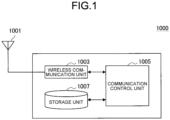
- FIG. 1 is a block diagram illustrating an example of a schematic functional configuration of the communication device according to the embodiment of the present disclosure.
- a communication device 1000 includes an antenna unit 1001, a wireless communication unit 1003, a storage unit 1007, and a communication control unit 1005.
- the antenna unit 1001 radiates, as a radio wave, a signal output by the wireless communication unit 1003 into a space. Further, the antenna unit 1001 converts a radio wave in the space into a signal and outputs the signal to the wireless communication unit 1003. Note that details of an example of an antenna device configuring the antenna unit 1001 will be described later.
- the wireless communication unit 1003 performs communication with another communication device via the antenna unit 1001. For example, the wireless communication unit 1003 may generate a transmission signal by modulating data to be transmitted based on a predetermined modulation method, and may transmit the transmission signal to another communication device via the antenna unit 1001. Further, the wireless communication unit 1003 may demodulate data transmitted from another communication device by acquiring a reception result of a signal transmitted from another communication device via the antenna unit 1001, and performing demodulation processing on the reception result.
- the storage unit 1007 temporarily or permanently stores a program and various data for operation of the communication device 1000.
- the communication control unit 1005 controls operation of the wireless communication unit 1003 to control communication with another communication device. For example, the communication control unit 1005 may control the operation of the wireless communication unit 1003 so that desired data is transmitted to another communication device. Further, the communication control unit 1005 may control the operation of the wireless communication unit 1003 so that data transmitted from another communication device is demodulated.
- IoT Internet of Things
- a technology called Internet of Things (IoT) that connects various things to a network
- IoT Internet of Things
- Such devices also include a device called a home appliance such as a television receiver.
- the shape and size of the antenna device for realizing wireless communication have been diversified, and in particular, in recent years, various antenna devices that can be built in a housing of a device have been proposed.
- an antenna device in a case where an antenna device is built in a housing of a communication device, a situation can be assumed in which the antenna device is installed in a limited space in the housing. In such a situation, the antenna device may be installed close to another metal component in the communication device, and thus, in this situation, a radiation pattern formed by the antenna device may be distorted due to an influence of the metal component. Therefore, in a case of assuming a situation in which the antenna device can be positioned close to another metal component, such as a case where the antenna device is built in the housing of the communication device, it is desired to implement an antenna device capable of further reducing an influence on the radiation pattern.
- a method of arranging a feeding point or feeding line for feeding power to an antenna element of the antenna device is limited.
- a feeding point of an antenna element for example, a radiation metal plate
- positions where a feeding pin and a feeding line for feeding, to the feeding point a feeding signal from a feeding circuit (for example, a component corresponding to the wireless communication unit 1003 illustrated in FIG. 1 ) may be limited.
- the feeding pin or feeding line is positioned in a radiation direction of the antenna element, the radiation pattern formed by the antenna element may be distorted. Therefore, in view of such a situation, it is more preferable that the feeding pin or feeding line is arranged so that the influence on the radiation pattern formed by the antenna element can be further reduced.
- FIGS. 2 to 5 are diagrams for describing an example of a configuration of the antenna device according to Comparative Example 1, and illustrate an example of a configuration of the antenna device capable of further reducing the influence on the radiation pattern even in a situation where the antenna device can be positioned close to a metal component.
- the antenna device according to Comparative Example 1 illustrated in FIGS. 2 to 5 is also referred to as an "antenna device 700" for convenience in order to distinguish the antenna device from an antenna device having a different configuration.
- FIG. 2 illustrates a schematic perspective view of the antenna device according to Comparative Example 1.
- the antenna device 700 according to Comparative Example 1 has a substantially flat plate shape.
- a normal direction of a plane (for example, an upper surface) of the substantially-flat-plate-shaped antenna device 700 will be referred to as a "Z direction”.
- two directions that is, a direction parallel to the plane of the substantially-flat-plate-shaped antenna device 700
- X direction a direction parallel to the plane of the substantially-flat-plate-shaped antenna device 700
- Y direction orthogonal to each other
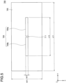
- FIG. 3 is a side view of the antenna device 700 illustrated in FIG. 2 , and illustrates the example of the schematic configuration of the antenna device 700 when viewed from the X direction.
- the antenna device 700 includes a metal layer 701, dielectric layers 703 and 705, a radiating element layer 707, and a non-contact feeding element 709.
- Reference Sign H71 indicates the thickness of the antenna device 700 in the Z direction.
- Reference Sign H73 indicates the thickness of the dielectric layer 703 in the Z direction.
- Reference Sign H75 indicates the thickness of the dielectric layer 705 in the Z direction.
- the dielectric layer 703 is formed in a substantially flat plate shape, and has one surface (a surface in the -z direction) on which the substantially-flat-plate-shaped metal layer 701 is formed so as to cover substantially the entire surface. Further, the radiating element layer 707 is provided on the other surface (a surface in the +z direction) of the dielectric layer 703.
- the +Z direction is also referred to as "upward” and the -Z direction is also referred to as "downward” for convenience. That is, among the respective surfaces of the dielectric layer 703, the surface in the +Z direction is also referred to as an "upper surface", and the surface in the -Z direction is also referred to as a "lower surface”.
- a portion of the antenna device 700 that is configured by stacking the metal layer 701, the dielectric layer 703, and the radiating element layer 707 is also referred to as a "lower layer portion 715" for convenience.
- FIG. 4 schematically illustrates a plan view of a portion corresponding to the lower layer portion 715 of the antenna device 700, which corresponds to an example of a configuration of the portion corresponding to the lower layer portion 715 when viewed from the +Z direction.
- Reference Sign W71 indicates the width of the antenna device 700 in the X direction.
- Reference Sign L71 indicates the width of the antenna device 700 in the Y direction.
- the radiating element layer 707 has a configuration corresponding to a so-called plate-shaped dipole antenna. That is, the radiating element layer 707 includes conductive antenna elements 707a and 707b each formed in a substantially flat plate shape. More specifically, the antenna elements 707a and 707b are arranged side by side along the Y direction above the upper surface (the surface in the +Z direction) of the dielectric layer 703 so that a slit 713 extending in the X direction is formed.
- Reference Sign L75 indicates the width of each of the antenna elements 707a and 707b in the Y direction. Further, Reference Sign L77 indicates the width of the slit 713 in the Y direction.
- the substantially-flat-plate-shaped dielectric layer 705 is stacked on the upper surface (the surface in the +Z direction) of the radiating element layer 707, and the non-contact feeding element 709 is arranged on the upper surface of the dielectric layer 705.
- a portion of the antenna device 700 that is arranged on the upper surface of the lower layer portion 715, that is, a portion including the dielectric layer 705 and the non-contact feeding element 709 is also referred to as an "upper layer portion 717" for convenience.
- FIG. 5 schematically illustrates a plan view of a portion corresponding to the upper layer portion 717 of the antenna device 700, which corresponds to an example of a configuration of the portion corresponding to the upper layer portion 717 when viewed from the +Z direction.
- the non-contact feeding element 709 has a configuration corresponding to a so-called dipole antenna, and is operated as a feeding element of the antenna device 700.
- the non-contact feeding element 709 includes conductive antenna elements 709a and 709b which are elongated so as to extend in a direction (Y direction) orthogonal to the direction (X direction) in which the slit 713 extends.
- a position corresponding to the center of the non-contact feeding element 709 is a feeding point 711 of the antenna device 700.
- Reference Sign W73 indicates the width of the non-contact feeding element 709 in the X direction.
- Reference Sign L73 indicates the width of the non-contact feeding element 709 in the Y direction.
- each condition is set under the assumption that the antenna device 700 transmits or receives a 2.45 GHz wireless signal.
- the width W71 in the X direction is 30 mm
- the width L71 in the Y direction is 55 mm
- the thickness H71 in the Z direction is 4 mm.
- the widths of the metal layer 701, the dielectric layer 703, the dielectric layer 705, and the radiating element layer 707 in the X direction and the Y direction are substantially equal to the width W71 of the antenna device 700 in the X direction and the width L71 of the antenna device 700 in the Y direction, respectively.
- the width L75 in the Y direction is 27.25 mm.
- the thickness H73 is 3.2 mm.
- the thickness H75 is 0.8 mm.
- those having a relative permittivity ⁇ r of 2.65 are used.
- the width W73 in the X direction is 1 mm and the width L73 in the Y direction is 26 mm.
- FIGS. 6 to 10 are diagrams each illustrating an example of a simulation result for each characteristic of the antenna device 700 according to Comparative Example 1.
- FIG. 6 is a diagram illustrating an example of a reflection characteristic simulation result of the antenna device 700 according to Comparative Example 1.
- a horizontal axis represents frequency (GHz) and a vertical axis represents reflection coefficient S11 (dB).
- reflection reflection coefficient S11
- FIG. 6 it can be seen that reflection (reflection coefficient S11) is significantly reduced at a frequency near 2.45 GHz, and the antenna device 700 according to Comparative Example 1 shows a favorable characteristic in a case where transmission or reception of a 2.45 GHz wireless signal is assumed.
- FIG. 7 is a Smith chart illustrating an example of an impedance characteristic simulation result of the antenna device 700 according to Comparative Example 1. As illustrated in FIG. 7 , it can be seen that the antenna device 700 according to Comparative Example 1 shows a capacitive characteristic.
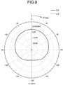
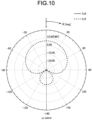
- FIGS. 8 to 10 are diagrams each illustrating an example of a radiation pattern simulation result of the antenna device 700 according to Comparative Example 1.
- a circumferential direction represents an angle (deg)
- a radial direction represents an operation gain (dBi)
- a solid line represents a ⁇ component of the operation gain
- a broken line represents a (
- FIG. 8 illustrates an example of the radiation pattern in a case where the radiation pattern of the antenna device 700 is cut along a plane parallel to an XY plane in FIG. 2
- FIG. 9 illustrates an example of the radiation pattern in a case where the radiation pattern of the antenna device 700 is cut along a plane parallel to an XZ plane in FIG. 2 .
- FIG. 10 illustrates an example of the radiation pattern in a case where the radiation pattern of the antenna device 700 is cut along a plane parallel to a YZ plane in FIG. 2 .
- the antenna device 700 according to Comparative Example 1 ideally forms a favorable radiation pattern with little distortion.
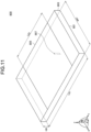
- FIG. 11 is a schematic perspective view of an antenna device according to Comparative Example 2, and is a view illustrating an example of a configuration of an antenna device configured as a so-called patch antenna.
- a normal direction of a plane (for example, an upper surface) of a substantially-flat-plate-shaped antenna device 800 will be referred to as a "Z direction”.
- two directions that is, a direction parallel to the plane of the substantially-flat-plate-shaped antenna device 800
- X direction a direction parallel to the plane of the substantially-flat-plate-shaped antenna device 800
- the +Z direction is also referred to as “upward” and the -Z direction is also referred to as “downward” for convenience.
- the antenna device according to Comparative Example 2 illustrated in FIG. 11 is also referred to as the “antenna device 800" for convenience in order to distinguish the antenna device from an antenna device having a different configuration.
- the antenna device 800 includes a metal base plate 801, a dielectric substrate 803, an antenna element 805, and a feeding portion 807.
- Reference Signs W81, L81, and H81 denote the width of the antenna device 800 in the X direction, the width of the antenna device 800 in the Y direction, and the thickness of the antenna device 800 in the Z direction, respectively.
- the dielectric substrate 803 is formed in a substantially flat plate shape, and the substantially-flat-plate-shaped metal base plate 801 is provided so as to cover substantially an entire lower surface (a surface in the -z direction). Further, the conductive antenna element 805 (that is, a radiation metal plate) formed in a flat plate shape is provided on an upper surface (a surface in the +z direction) of the dielectric substrate 803. Reference Sign L83 indicates the width of the antenna element 805 in the Y direction. Further, the feeding portion 807 is provided so that a part of the antenna element 805 is used as a feeding point and power is fed from the lower surface side (that is, a side facing the dielectric substrate 803) of the antenna element 805 to the feeding point.
- the feeding portion 807 includes, for example, a feeding pin and a feeding line that supplies a feeding signal from a feeding circuit to the feeding pin. It is a matter of course that a configuration of the feeding portion 807 is not particularly limited as long as power can be fed to the feeding point.
- each condition is set under the assumption that the antenna device 800 transmits or receives a 2.45 GHz wireless signal.
- the width W81 in the X direction is 35 mm
- the width L71 in the Y direction is 55 mm
- the thickness H71 in the Z direction is 4 mm.
- the widths of the metal base plate 801 and the dielectric substrate 803 in the X direction and the Y direction are substantially equal to the width W81 of the antenna device 800 in the X direction and the width L81 of the antenna device 800 in the Y direction, respectively.
- the width of the antenna element 805 in the X direction is substantially equal to the width W81 of the antenna device 800 in the X direction, and the width L83 in the Y direction is 35 mm. Further, as the dielectric substrate 803, one having a relative permittivity ⁇ r of 2.65 is used.
- FIGS. 12 to 16 each illustrate an example of a simulation result for each characteristic of the antenna device 800 according to Comparative Example 2.
- FIG. 12 is a diagram illustrating an example of a reflection characteristic simulation result of the antenna device 800 according to Comparative Example 2.
- a horizontal axis represents frequency (GHz) and a vertical axis represents reflection coefficient S11 (dB).
- reflection reflection coefficient S11
- FIG. 12 it can be seen that reflection (reflection coefficient S11) is significantly reduced at a frequency near 2.45 GHz, and the antenna device 800 according to Comparative Example 2 shows a favorable characteristic in a case where transmission or reception of a 2.45 GHz wireless signal is assumed.
- the antenna device 800 according to Comparative Example 2 and the above-described antenna device 700 according to Comparative Example 1 have similar reflection characteristics.
- FIG. 13 is a Smith chart illustrating an example of an impedance characteristic simulation result of the antenna device 800 according to Comparative Example 2. As illustrated in FIG. 8 , it can be seen that the antenna device 800 according to Comparative Example 2 shows an inductive characteristic.
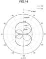
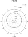
- FIGS. 14 to 16 are diagrams each illustrating an example of a radiation pattern simulation result of the antenna device 800 according to Comparative Example 2.
- a circumferential direction represents an angle (deg)
- a radial direction represents an operation gain (dBi)
- a solid line represents a ⁇ component of the operation gain
- a broken line represents a (
- FIG. 14 illustrates an example of the radiation pattern in a case where the radiation pattern of the antenna device 800 is cut along a plane parallel to an XY plane in FIG. 11
- FIG. 15 illustrates an example of the radiation pattern in a case where the radiation pattern of the antenna device 800 is cut along a plane parallel to an XZ plane in FIG. 11 .
- FIG. 16 illustrates an example of the radiation pattern in a case where the radiation pattern of the antenna device 800 is cut along a plane parallel to a YZ plane in FIG. 11 .
- the antenna device 800 according to Comparative Example 2 and the above-described antenna device 700 according to Comparative Example 1 form similar radiation patterns.
- the antenna device 700 according to Comparative Example 1 and the antenna device 800 according to Comparative Example 2 have substantially the same dimensions and relatively similar characteristics, except for the impedance characteristic.
- FIG. 17 is a diagram for describing an outline of a method of simulating a behavior when an antenna device is brought close to a metal. Specifically, a simulation is performed to check, in a case where a metal plate 690 is disposed below an antenna device (that is, the antenna device 700 or 800) as a simulation target, how the characteristics of the antenna device are changed depending on a distance d between the antenna device and the metal plate 690. Note that the metal plate 690 is assumed to be an electrically perfect conductor having an infinite size in an XY plane direction. Further, the simulation for each characteristic of the antenna device is performed when the distance d is 0 mm, 10 mm, 20 mm, and 30 mm, respectively.
- FIG. 18 is a diagram illustrating an example of a reflection characteristic simulation result of the antenna device 700 according to Comparative Example 1. Note that a vertical axis and a horizontal axis in FIG. 18 are the same as those in the examples illustrated in FIGS. 6 and 12 . As illustrated in FIG. 18 , it can be seen that the characteristic of the antenna device 700 according to Comparative Example 1 is hardly changed regardless of proximity to the metal plate 690, except for a case where the distance d is 0 mm (that is, a case where the antenna device 700 and the metal plate 690 are in contact with each other).
- FIG. 19 is a diagram illustrating an example of a reflection characteristic simulation result of the antenna device 800 according to Comparative Example 2. Note that a vertical axis and a horizontal axis in FIG. 19 are the same as those in the example illustrated in FIG. 18 . As illustrated in FIG. 19 , it can be seen that the characteristic of the antenna device 800 according to Comparative Example 2 is hardly changed regardless of proximity to the metal plate 690, except for a case where the distance d is 0 mm (that is, a case where the antenna device 800 and the metal plate 690 are in contact with each other). That is, as can be seen by comparing FIGS.
- the antenna device 700 according to Comparative Example 1 and the antenna device 800 according to Comparative Example 2 are similar in respect to an aspect of the change in reflection characteristic (that is, an influence on the reflection characteristic) when the metal plate 690 is brought close to the antenna device 700 according to Comparative Example 1 and the antenna device 800 according to Comparative Example 2.
- FIG. 20 is a diagram illustrating an example of an impedance characteristic simulation result of the antenna device 700 according to Comparative Example 1. As illustrated in FIG. 18 , it can be seen that the characteristic of the antenna device 700 according to Comparative Example 1 is hardly changed regardless of proximity to the metal plate 690, except for a case where the distance d is 0 mm.
- FIG. 21 is a diagram illustrating an example of an impedance characteristic simulation result of the antenna device 800 according to Comparative Example 2.
- the characteristic of the antenna device 800 according to Comparative Example 2 is hardly changed regardless of proximity to the metal plate 690, except for a case where the distance d is 0 mm. That is, as can be seen by comparing FIGS. 20 and 21 , the antenna device 700 according to Comparative Example 1 and the antenna device 800 according to Comparative Example 2 are similar in respect to an aspect of the change in impedance characteristic (that is, an influence on the impedance characteristic) when the metal plate 690 is brought close to the antenna device 700 according to Comparative Example 1 and the antenna device 800 according to Comparative Example 2.
- FIG. 22 is a diagram for describing an outline of an example of a power feeding method of the antenna device 700 according to Comparative Example 1.
- examples of the power feeding method of the antenna device 700 according to Comparative Example 1 include "a method of feeding power from the upper surface side", “a method of feeding power from the lower surface side”, and “a method of feeding power from the side surface side”. Therefore, an outline of each power feeding method will be described below.
- the feeding line is arranged so as to be positioned on the upper surface side (+Z direction side) of the antenna device 700, and power is fed from the upper surface side of the antenna device 700 to the feeding point 711 via the feeding line. Due to such characteristics, in a case of adopting this method, at least a part of a radiation pattern of a wireless signal that is formed by the antenna device 700 is blocked by the feeding line, which may disturb the radiation pattern.
- the feeding line is arranged so as to be positioned on the lower surface side (-Z direction side) of the non-contact feeding element 709, and power is fed from the lower surface side of the non-contact feeding element 709 to the feeding point 711 via the feeding line. Due to such characteristics, in a case of adopting this method, for example, the feeding line is arranged so as to penetrate through the radiating element layer 707 in the Z direction, and a part of the feeding line is interposed between the radiating element layer 707 and the non-contact feeding element 709. Therefore, a part of the feeding line may interfere with a radiating electric field formed by the radiating element layer 707, and may affect the radiation pattern.
- the feeding line is arranged so as to be positioned on the side surface side (for example, X direction side) of the non-contact feeding element 709, and power is fed from the side surface side of the non-contact feeding element 709 to the feeding point 711 via the feeding line. Due to such characteristics, in a case of adopting this method, it is possible to prevent a situation where the radiation pattern is blocked by the feeding line. On the other hand, since the feeding line is arranged so as to extend from the feeding point 711 toward any side in the X direction, the radiation pattern may be disturbed due to asymmetry in the X direction.
- the antenna device 700 according to Comparative Example 1 needs to perform balanced power feeding, and has a low affinity with a power feeding method using a so-called microstrip line.
- the antenna device 700 according to Comparative Example 1 is characterized in that the characteristics are hardly changed even in a situation where a metal is brought close to the antenna device 700.
- the degree of freedom in design may be decreased in a case of application to the communication device according to the embodiment of the present disclosure.
- the present disclosure proposes a technology for implementing an antenna device capable of further reducing an influence of proximity to a metal and feeding power to an antenna element in a more suitable manner.
- FIGS. 23 and 24 are views for describing the configuration of the antenna device according to the embodiment of the present disclosure. Note that, in the following description, the antenna device according to the present embodiment illustrated in FIGS. 23 and 24 is also referred to as an "antenna device 100" for convenience in order to distinguish the antenna device from an antenna device having a different configuration.
- FIG. 23 is a schematic perspective view of the antenna device according to the embodiment of the present disclosure.
- the antenna device 100 according to the present embodiment has a substantially flat plate shape.
- a normal direction of a plane (for example, an upper surface) of a substantially-flat-plate-shaped antenna device 100 will be referred to as a "Z direction”.
- two directions that is, a direction parallel to the plane of the substantially-flat-plate-shaped antenna device 100
- X direction a direction parallel to the plane of the substantially-flat-plate-shaped antenna device 100
- the antenna device 100 includes a metal base plate 101, a dielectric substrate 103, antenna elements 105a and 105b, and feeding portions 109a and 109b.
- Reference Signs W11, L11, and H11 denote the width of the antenna device 100 in the X direction, the width of the antenna device 100 in the Y direction, and the thickness of the antenna device 100 in the Z direction, respectively.
- the dielectric substrate 103 is formed in a substantially flat plate shape, and the substantially-flat-plate-shaped metal base plate 101 is provided so as to cover substantially an entire lower surface (a surface in the -z direction). Further, the conductive antenna elements 105a and 105b (that is, radiation metal plates) formed in a flat plate shape are provided on an upper surface (a surface in the +z direction) of the dielectric substrate 103 so that a slit 107 is formed. Specifically, in the example illustrated in FIG. 23 , the antenna elements 105a and 105b are arranged side by side in the Y direction so that the slit 107 extending in the X direction is formed. Here, the antenna elements 105a and 105b are arranged so as to be electrically separated from each other.
- the antenna elements 105a and 105b are arranged so as to be spatially separated along the Y direction, and thus are electrically separated from each other.
- the antenna elements 105a and 105b may be simply referred to as an "antenna element 105" unless otherwise distinguished.
- a surface (lower surface) on which the metal base plate 101 is provided corresponds to an example of a "first surface”
- a surface (upper surface) on which the antenna elements 105a and 105b are arranged corresponds to an example of a "second surface”.
- the antenna elements 105a and 105b are arranged so that the width of the slit 107 (that is, the width in the Y direction) is at least smaller than 1/2 of a wavelength of a wireless signal transmitted or received by the antenna elements 105a and 105b.
- the configuration of the antenna device 100 is different from a so-called array antenna.
- the antenna elements 105a and 105b are preferably arranged so that the width of the slit 107 is 1/40 or less of the wavelength of the wireless signal transmitted or received by the antenna elements 105a and 105b.
- the antenna elements 105a and 105b may be formed so that a surface (for example, an upper surface corresponding to a radiation surface) extending along the upper surface of the dielectric substrate 103 has a substantially rectangular shape.
- the length of the surface in the Y direction (that is, the length in a direction orthogonal to the slit 107) is substantially equal to the length L y shown in (Equation 1) below.
- ⁇ represents a wavelength of a transmitted or received wireless signal.
- ⁇ r represents relative permittivity of the dielectric substrate.
- the antenna elements 105a and 105b are preferably arranged so that the width of the slit 107 is 1/10 or less of the length of one side of the surface.
- L y 0.4 ⁇ / ⁇ r
- the feeding portion 109a is provided so that a part of the antenna element 105a is used as a feeding point and power is fed to the feeding point.
- the feeding portion 109b is provided so that a part of the antenna element 105b is used as a feeding point and power is fed to the feeding point.
- each feeding point is preferably set so that a direction from one of the feeding points of the antenna elements 105a and 105b to the other and a direction in which the slit 107 extends are substantially orthogonal to each other (that is, it is preferable that the feeding portions 109a and 109b are provided).
- the feeding portions 109a and 109b include, for example, a feeding pin and a feeding line that supplies a feeding signal from a feeding circuit to the feeding pin.
- each of the feeding portions 109a and 109b is not particularly limited as long as power can be fed to each feeding point.
- the feeding portions 109a and 109b may be simply referred to as a "feeding portion 109" unless otherwise distinguished.
- one of the antenna elements 105a and 105b corresponds to an example of a "first antenna element”, and the other corresponds to an example of a "second antenna element”.
- a feeding portion 109 that feeds power to the first antenna element corresponds to an example of a "first feeding portion”
- a feeding portion 109 that feeds power to the second antenna element corresponds to an example of a "second power feeding portion”.
- the direction in which the slit 107 extends corresponds to an example of a "first direction”.
- a direction from one of the feeding points of the respective antenna elements 105a and 105b to the other corresponds to a "second direction".
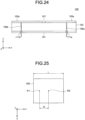
- FIG. 24 is a schematic cross-sectional view of the antenna device 100 illustrated in FIG. 23 , and is a cross-sectional view when viewed from the X direction in a case where the antenna device 100 is cut along a plane parallel to a ZY plane including the feeding portions 109a and 109b.
- the feeding portion 109a is arranged so as to be electrically connected to the lower surface side of the antenna element 105a.
- a hole portion 111a penetrating in the Z direction is provided in a part of the metal base plate 101 that is positioned below the antenna element 105a.
- the feeding portion 109a extends from the lower surface side of the metal base plate 101 so as to penetrate the metal base plate 101 through the hole portion 111a, and is electrically connected to the lower surface side of the antenna element 105a.
- the feeding portion 109a is electrically connected to the lower surface side of the antenna element 105a while being separated from the metal base plate 101.
- an upper end of the feeding portion 109a is positioned below the radiation surface of the antenna element 105a.
- the feeding portion 109b is arranged so as to be electrically connected to the lower surface side of the antenna element 105b.
- a hole portion 111b penetrating in the Z direction is provided in a part of the metal base plate 101 that is positioned below the antenna element 105b.
- the feeding portion 109b extends from the lower surface side of the metal base plate 101 so as to penetrate the metal base plate 101 through the hole portion 111b, and is electrically connected to the lower surface side of the antenna element 105b.
- the feeding portion 109b is electrically connected to the lower surface side of the antenna element 105b while being separated from the metal base plate 101.
- an upper end of the feeding portion 109b is positioned below the radiation surface of the antenna element 105b.
- a control is performed so that a phase difference between feeding signals supplied to the feeding portions 109a and 109b, respectively, is approximately 180 degrees.
- the feeding signals whose phases are different by 180 degrees are fed to the feeding points of the antenna elements 105a and 105b, respectively.
- the antenna device 100 forms a radiation pattern on the upper surface side (that is, +Z direction side) of each antenna element 105 based on the power feeding from each feeding portion 109.
- the configuration of the antenna device 100 illustrated in FIG. 24 is merely an example, and as long as it is possible to feed power to the antenna element 105, the method of arranging the feeding portion 109 is not necessarily limited to the example illustrated in FIG. 24 . That is, as long as it is possible to arrange the feeding portion 109 so that the radiation pattern formed by the antenna device 100 is not blocked by the feeding portion 109, the method of arranging the feeding portion 109 is not particularly limited.
- the feeding portion 109 may be arranged so as to extend from a side portion of the dielectric substrate 103 (for example, a side portion in the X direction or the Y direction) toward the lower side of the antenna element 105, and a portion of the feeding portion 109 that is positioned below the antenna element 105 may be electrically connected to the lower surface side of the antenna element 105. Further, the feeding portion 109 may be arranged so that the feeding portion 109 is electrically connected to the side portion of the antenna element 105 (for example, the side portion in the X direction or the Y direction) on the upper surface side of the dielectric substrate 103. Note that an example of a method of arranging the feeding portion 109 will be separately described later in detail as a modified example.
- the position of the feeding point in the antenna element 105 (radiation metal plate) will be described in more detail.
- the position of the feeding point is determined depending on impedance that matches input impedance R in to the antenna element 105.
- FIG. 25 is a diagram for describing a method of setting a position of a feeding point in the antenna device according to the present embodiment.
- FIG. 25 is a schematic plan view of the antenna element 105 when viewed from the Z direction.
- Reference Sign P0 schematically indicates the center (that is, the center in the X direction and the Y direction) of the upper surface of the antenna element 105 formed in a substantially flat plate shape.
- Reference Sign P1 schematically indicates the position of the feeding point.
- the input impedance R in of the antenna element 105 in a case where the feeding point P1 is separated from the center P0 of the antenna element 105 by a distance Xf is represented by the following calculation formula (Equation 1).
- R r represents the input impedance of the antenna element 105 in a case where power is fed at an end (for example, an end in the Y direction) of the antenna element 105.
- Reference Sign L schematically represents the width of the antenna element 105 in a direction in which the feeding point P1 is moved.
- the example illustrated in FIG. 25 shows a case where the feeding point P1 is moved so as to be separated from the center P0 of the antenna element 105 along the Y direction, in order to make the features of the antenna device according to the present embodiment easier to understand. That is, in the example illustrated in FIG. 25 , L indicates the width of the antenna element 105 in the Y direction.
- the input impedance R in of the antenna element 105 is ideally calculated based on (Equation 1) above.
- the position of the feeding point P1 is preferably determined (the distance X f is determined) so that the input impedance R in of the antenna element 105 matches a desired impedance (for example, 50 ⁇ ) by performing an electromagnetic field analysis using X f described above as a parameter.
- FIG. 26 is a block diagram illustrating an example of a functional configuration of the wireless communication unit that drives the antenna device according to the present embodiment.
- an antenna unit 1001 and a wireless communication unit 1003 illustrated in FIG. 26 can correspond to the antenna unit 1001 and the wireless communication unit 1003 described with reference to FIG. 1 .
- FIG. 26 illustrates an example of a functional configuration of the wireless communication unit 1003 in a case where the antenna device 100 according to the present embodiment is applied as the antenna unit 1001 of the communication device 1000 illustrated in FIG. 1 . Therefore, in the example illustrated in FIG. 26 , the antenna unit 1001 includes two feeding pins 1011a and 1011b. That is, the feeding pins 1011a and 1011b schematically indicate, for example, the feeding pins included in the feeding portions 109a and 109b illustrated in FIGS. 23 and 25 , and are arranged so that power is fed to different antenna elements.
- the wireless communication unit 1003 includes a transmitter 1013, a modulation circuit 1015, a power amplifier (PA) 1017, a switch 1019, a filter 1021, a distributor 1023, and a phase circuit 1025, a low noise amplifier (LNA) 1027, a demodulation circuit 1029, and a receiver 1031 as illustrated in FIG. 26 .
- PA power amplifier
- LNA low noise amplifier
- the transmitter 1013, the modulation circuit 1015, and the PA 1017 are components for generating a drive signal (in other words, a feeding signal) that drives the antenna unit 1001 in order to transmit a wireless signal corresponding to data to be transmitted from the antenna unit 1001.
- the drive signal is generated by modulating, by the modulation circuit 1015, an electric signal with a desired frequency that is generated by the transmitter 1013 according to the data to be transmitted, and amplifying, by the PA 1017, the modulated electric signal.
- the generated drive signal is input to the switch 1019.
- the switch 1019 is a component for selectively switching a supply destination (in other words, a signal transmission path) of the input electric signal.
- the switch 1019 controls the signal transmission path so that the drive signal output from the PA 1017 is transmitted to the distributor 1023 via the filter 1021 during an operation related to transmission of a wireless signal.
- the switch 1019 controls the signal transmission path so that a reception signal output from the filter 1021 according to a reception result of an antenna unit 1011 is transmitted to the demodulation circuit 1029 via the LNA 1027 during an operation related to reception of a wireless signal.
- the filter 1021 passes a signal in a predetermined frequency band among input signals and blocks a signal in another frequency band.
- the filter 1021 may be configured as a so-called low-pass filter. In such a case, the filter 1021 passes a low frequency component (that is, a signal having a frequency equal to or lower than a threshold) of the input signal and blocks a high frequency component. This makes it possible to remove a so-called noise component included in a signal input to the filter 1021.
- the drive signal generated by the transmitter 1013, the modulation circuit 1015, and the PA 101 is input to the filter 1021 via the switch 1019, a noise component is removed by the filter 1021, and then the signal is demultiplexed by the distributor 1023.
- One of drive signals demultiplexed by the distributor 1023 is supplied to the feeding pin 1011a via the phase circuit 1025.
- the phase circuit 1025 shifts the phase of the input drive signal by 180 degrees.
- the other drive signal is supplied to the feeding pin 1011b.
- a phase difference between the drive signal supplied to the feeding pin 1011a and the drive signal supplied to the feeding pin 1011b is 180 degrees.
- the drive signal (in other words, the feeding signal) supplied to each of the feeding pins 1011a and 1011b drives an antenna element of the antenna unit 1001, and a wireless signal corresponding to the drive signal is radiated from the antenna element.
- an electric signal (hereinafter, also referred to as a "reception signal") corresponding to the wireless signal is input to the wireless communication unit 1003 via the feeding pins 1011a and 1011b.
- the phase of the reception signal input via the feeding pin 1011a is shifted by 180 degrees by the phase circuit 1025.
- the reception signal input from each of the feeding pins 1011a and 1011b is input to the switch 1019 via the distributor 1023 and the filter 1021.
- the filter 1021 for example, a high frequency component (noise component) included in the reception signal may be removed.
- the switch 1019 controls the signal transmission path so that a reception signal output from the filter 1021 according to a reception result of the antenna unit 1011 is transmitted to the demodulation circuit 1029 via the LNA 1027 during an operation related to reception of a wireless signal.
- the reception signal output from the switch 1019 is amplified by the LNA 1027, demodulated by the demodulation circuit 1029, and then received by the receiver 1031. That is, data corresponding to the reception signal is received.
- the functional configuration of the wireless communication unit 1003 is not necessarily limited to the example illustrated in FIG. 26 as long as it is possible to implement operations related to transmission and reception of a wireless signal.
- the antenna unit 1001 and at least some components of the wireless communication unit 1003 may be integrated with each other.
- some of the respective components of the wireless communication unit 1003 may be provided outside the wireless communication unit 1003.
- the function of the wireless communication unit 1003 may be implemented by a plurality of devices (for example, a plurality of chips) operating in cooperation with each other.
- Example an antenna characteristic simulation result of the antenna device according to the embodiment of the present disclosure will be summarized below.
- the antenna device 100 according to the present embodiment is driven by driving the feeding circuit (for example, the wireless communication unit 1003 illustrated in FIG. 26 ) under the same conditions as in a case where it is assumed that a 2.45 GHz wireless signal is transmitted or received by the antenna device 700 according to Comparative Example 1.
- the feeding circuit for example, the wireless communication unit 1003 illustrated in FIG. 26
- FIGS. 27 to 33 each illustrate an example of a simulation result for each characteristic of the antenna device 700 according to Comparative Example 1.
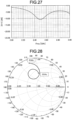
- FIG. 27 is a diagram illustrating an example of a reflection characteristic simulation result of the antenna device 100 according to Example of the embodiment of the present disclosure.
- a horizontal axis represents frequency (GHz) and a vertical axis represents reflection coefficient S11 (dB).
- the antenna device 100 according to Example has a slightly smaller resonance depth, as compared with the antenna device 700 according to Comparative Example 1. However, it is considered that the same characteristic of the antenna device 100 (that is, a characteristic difference between the antenna device 100 and the antenna device 700) is within a range adjustable according to the matching.
- FIG. 28 is a Smith chart illustrating an example of an impedance characteristic simulation result of the antenna device 100 according to Example of the embodiment of the present disclosure. As illustrated in FIG. 28 , it can be seen that the antenna device 100 according to Example shows an inductive characteristic.
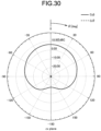
- FIGS. 29 to 31 are diagrams each illustrating an example of the radiation pattern simulation result of the antenna device according to Example of the embodiment of the present disclosure.
- a circumferential direction represents an angle (deg)
- a radial direction represents an operation gain (dBi)
- a solid line represents a ⁇ component of the operation gain
- a broken line represents a ⁇ component of the operation gain.
- FIG. 29 illustrates an example of the radiation pattern in a case where the radiation pattern of the antenna device 100 is cut along a plane parallel to an XY plane in FIG. 23 .
- FIG. 29 illustrates an example of the radiation pattern in a case where the radiation pattern of the antenna device 100 is cut along a plane parallel to an XY plane in FIG. 23 .
- FIG. 30 illustrates an example of the radiation pattern in a case where the radiation pattern of the antenna device 100 is cut along a plane parallel to an XZ plane in FIG. 23 .
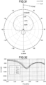
- FIG. 31 illustrates an example of the radiation pattern in a case where the radiation pattern of the antenna device 100 is cut along a plane parallel to a YZ plane in FIG. 23 .
- the radiation pattern of the antenna device 100 according to Example is similar to the radiation pattern of the antenna device 700 according to Comparative Example 1.
- FIGS. 32 and 33 simulation results of an influence on characteristics when the antenna device 100 according to Example of the embodiment of the present disclosure is brought close to a metal will be described with reference to FIGS. 32 and 33 .
- a method of the simulation is performed under the same conditions as in a case of the simulation of the antenna device 700 according to Comparative Example 1 and the antenna device 800 according to Comparative Example 2 described above. That is, as illustrated in FIG. 17 , a simulation is performed to check, in a case where the metal plate 690 is disposed below an antenna device (that is, the antenna device 100) as a simulation target, how the characteristics of the antenna device are changed depending on a distance d between the antenna device and the metal plate 690.
- the metal plate 690 is assumed to be an electrically perfect conductor having an infinite size in an XY plane direction. Further, the simulation for each characteristic of the antenna device is performed when the distance d is 0 mm, 10 mm, 20 mm, and 30 mm, respectively.
- FIG. 32 is a diagram illustrating an example of a reflection characteristic simulation result of the antenna device according to Example of the embodiment of the present disclosure. Note that a vertical axis and a horizontal axis in FIG. 32 are the same as those in the example illustrated in FIG. 27 .
- the reflection characteristic of the antenna device 100 according to the present embodiment is hardly changed regardless of proximity to the metal plate 690.
- a change in reflection characteristic of the antenna device 100 according to Example when a metal is brought close to the antenna device 100 is smaller, as compared with the antenna device 800 according to Comparative Example 2.
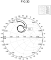
- FIG. 33 is a Smith chart illustrating an example of an impedance characteristic simulation result of the antenna device according to Example of the embodiment of the present disclosure.
- the impedance characteristic of the antenna device 100 according to the present embodiment is hardly changed regardless of proximity to the metal plate 690.
- a change in impedance characteristic of the antenna device 100 according to Example when a metal is brought close to the antenna device 100 is smaller, as compared with the antenna device 800 according to Comparative Example 2.
- the antenna device 100 according to Example can implement the same antenna characteristics as the antenna device 700. Further, the antenna device 100 according to the present embodiment can suppress a change in various characteristics when a metal is brought close to the antenna device 100 to the same extent or more as compared with the antenna device 800 according to Comparative Example 2. Further, in the antenna device 100 according to the present embodiment, it is possible to arrange the feeding portion 109 so that the radiation pattern is not blocked by the feeding portion 109 (for example, the feeding pin or feeding line) in consideration of the configuration characteristics described with reference to FIGS. 23 and 24 .
- the power feeding method of the antenna device 100 according to the present embodiment is the unbalanced power feeding, the antenna device 100 has a high affinity with a general microstrip line. That is, even in a situation where the antenna device is installed in a limited space inside the housing of the communication device, an influence of proximity to a metal can be further reduced, and power can be fed to the antenna element in a more suitable manner.
- FIG. 34 is a view for describing an example of a configuration of the antenna device according to Modified Example 1, and is a schematic perspective view of the antenna device.
- the antenna device according to Modified Example 1 may be referred to as an "antenna device 130" when it is particularly distinguished from the antenna device 100 according to the above-described embodiment.
- An X direction, a Y direction, and a Z direction in FIG. 34 are the same as the X direction, the Y direction, and the Z direction in FIG. 23 .
- the antenna device 130 includes a metal base plate 131, a dielectric substrate 133, antenna elements 135a and 135b, and feeding portions 139a and 139b.
- configurations of the metal base plate 131, the dielectric substrate 133, the antenna element 135a, and the antenna element 133b are substantially the same as the metal base plate 101, the dielectric substrate 103, the antenna element 105a, and the antenna element 105b in the antenna device 100 illustrated in FIG. 23 .
- Reference Sign 137 indicates a slit formed between the antenna elements 135a and 135b, and corresponds to the slit 107 in the antenna device 100 illustrated in FIG. 23 .
- the configuration of the antenna device 130 according to Modified Example 1 will be described focusing on a difference from the antenna device 100 according to the above-described embodiment, and a detailed description of the metal base plate 131, the dielectric substrate 133, the antenna elements 135a and 135b, and the slit 137 that are substantially the same as those of the antenna device 100 is omitted.
- the feeding portion 139a includes a pad 143a. Specifically, a portion corresponding to a feeding line of the feeding portion 139a is electrically connected to the pad 143a. Based on such a configuration, a feeding signal is supplied to the pad 143a via the portion corresponding to the feeding line of the feeding portion 139a, and power is fed from the pad 143a to a feeding point of the antenna element 135a by non-contact power feeding.
- the pad 143a corresponding to an upper end of the feeding portion 139a is positioned below a radiation surface of the antenna element 135a.
- the feeding portion 139b includes a pad 143b. Specifically, a portion corresponding to a feeding line of the feeding portion 139b is electrically connected to the pad 143b. Based on such a configuration, a feeding signal is supplied to the pad 143b via the portion corresponding to the feeding line of the feeding portion 139b, and power is fed from the pad 143b to a feeding point of the antenna element 135b by non-contact power feeding.
- the pad 143b corresponding to an upper end of the feeding portion 139b is positioned below a radiation surface of the antenna element 135b.
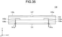
- FIG. 35 is a schematic cross-sectional view of the antenna device 130 illustrated in FIG. 34 , and is a cross-sectional view when viewed from the X direction in a case where the antenna device 130 is cut along a plane parallel to a ZY plane including the feeding portions 139a and 139b.
- the pad 143a is formed in a substantially flat plate shape. Further, as illustrated in FIG. 35 , the pad 143a is interposed between the antenna element 135a and the metal base plate 131, and is arranged so that an upper surface of the pad 143a faces a lower surface of the antenna element 135a. Further, a portion corresponding to the feeding line of the feeding portion 139a penetrates the metal base plate 131 through a hole portion 141a provided in the metal base plate 131 while being electrically separated from the metal base plate 131, and is electrically connected to the lower surface side of the pad 143a.
- the pad 143b is formed in a substantially flat plate shape. Further, the pad 143b is interposed between the antenna element 135b and the metal base plate 131, and is arranged so that an upper surface of the pad 143b faces a lower surface of the antenna element 135b. Further, a portion corresponding to the feeding line of the feeding portion 139b penetrates the metal base plate 131 through a hole portion 141b provided in the metal base plate 131 while being electrically separated from the metal base plate 131, and is electrically connected to the lower surface side of the pad 143b.
- a connection relationship between the pad 143a and the portion corresponding to the feeding line of the feeding portion 139a is not particularly limited.
- the feeding line is electrically connected to an end of the pad 143a in the Y direction so that the pad 143a and the portion corresponding to the feeding line of the feeding portion 139a form an L shape on a YZ plane.
- the feeding line may be electrically connected to a portion in the vicinity of the center of the pad 143a in the Y direction so that the pad 143a and the portion corresponding to the feeding line of the feeding portion 139a form a T shape on the YZ plane.
- Modified Example 1 an example of the configuration of the antenna device according to the present embodiment in a case where the antenna device is configured to perform power feeding by non-contact power feeding has been described with reference to FIGS. 34 and 35 .
- FIG. 36 is a view for describing an example of a configuration of the antenna device according to Modified Example 2, and is a schematic perspective view of the antenna device.
- the antenna device according to Modified Example 2 may be referred to as an "antenna device 150" when it is particularly distinguished from the antenna device 100 according to the above-described embodiment.
- An X direction, a Y direction, and a Z direction in FIG. 36 are the same as the X direction, the Y direction, and the Z direction in FIG. 23 .
- the antenna device 150 includes a metal base plate 151, a dielectric substrate 153, and antenna elements 155a and 155b. Note that configurations of the metal base plate 151 and the dielectric substrate 153 are substantially the same as those of the metal base plate 101 and the dielectric substrate 103 in the antenna device 100 illustrated in FIG. 23 . Further, Reference Sign 157 indicates a slit formed between the antenna elements 155a and 155b, and corresponds to the slit 107 in the antenna device 100 illustrated in FIG. 23 .
- the configuration of the antenna device 150 according to Modified Example 2 will be described focusing on a difference from the antenna device 100 according to the above-described embodiment, and a detailed description of the metal base plate 151, the dielectric substrate 153, and a slit 157 that are substantially the same as those of the antenna device 100 is omitted.
- the antenna element 155a is formed on the dielectric substrate 153 so that a portion of the antenna element 155a extends in the +Y direction (that is, a direction along an upper surface of the dielectric substrate 153), and the extending portion serves as a feeding portion. Therefore, hereinafter, the portion of the antenna element 155a that is formed so as to extend in the +Y direction is also referred to as a "feeding portion 159a" for convenience. That is, on the dielectric substrate 153, the feeding portion 159a is electrically connected to a side portion of a portion corresponding to a radiation metal plate of the antenna element 155a.
- the feeding portion 159a is arranged so that a position of an upper surface of the feeding portion 159a in the Z direction is on substantially the same level as a position of a radiation surface (that is, upper surface) of the antenna element 155a, or is on a level lower than the radiation surface (that is, on a side opposite to a direction in which the antenna element 155a radiates a wireless signal).
- a direction in which the antenna element 155a radiates a wireless signal that is, upward
- a direction (that is, downward) opposite to the direction corresponds to an example of a "fourth direction”.
- the antenna element 155b is formed on the dielectric substrate 153 so that a portion of the antenna element 155b extends in the -Y direction (that is, the direction along the upper surface of the dielectric substrate 153), and the extending portion serves as a feeding portion. Therefore, hereinafter, the portion of the antenna element 155b that is formed so as to extend in the -Y direction is also referred to as a "feeding portion 159bv for convenience. That is, on the dielectric substrate 153, the feeding portion 159b is electrically connected to a side portion of a portion corresponding to a radiation metal plate of the antenna element 155b.
- the feeding portion 159b is arranged so that a position of an upper surface of the feeding portion 159b in the Z direction is on substantially the same level as a position of a radiation surface (that is, upper surface) of the antenna element 155b, or is on a level lower than the radiation surface (that is, on a side opposite to a direction in which the antenna element 155a radiates a wireless signal).
- the feeding portions 159a and 159b may be configured as a microstrip line.
- antenna characteristic matching is performed by providing a notch in the vicinity of a portion where the feeding portion 159a is provided, in a portion corresponding to the radiation metal plate of the antenna element 155a. That is, the antenna characteristic matching may be performed by performing an electromagnetic field analysis using at least some of the depth, the width, and the like of the notch as a parameter. Similarly, the antenna characteristic matching is performed by providing a notch also in the vicinity of a portion where the feeding portion 159b is provided, in a portion corresponding to the radiation metal plate of the antenna element 155b.
- Power is fed to each of the feeding portions 159a and 159b based on the above configuration.
- a control is performed so that a phase difference between feeding signals supplied to the feeding portions 159a and 159b, respectively, is approximately 180 degrees.
- a method of arranging a feeding circuit that feeds power to the antenna elements 155a and 155b via the feeding portions 159a and 159b is not particularly limited.
- a portion corresponding to the feeding circuit may be arranged on the dielectric substrate 153, similarly to the feeding portions 159a and 159b.
- the portion corresponding to the feeding circuit is arranged so that a position of an upper surface of the portion in the Z direction is on substantially the same level as a position of a radiation surface (that is, upper surface) of each of the antenna elements 155a and 155b, or is on a level lower than the radiation surface. It is a matter of course that the above is merely an example, and the position where the portion corresponding to the feeding circuit is arranged is not limited.
- Modified Example 2 an example of the configuration of the antenna device according to the present embodiment in a case where the antenna device is configured to perform power feeding on the dielectric substrate has been described with respect to FIG. 36 .
- FIG. 37 is a view for describing an example of a configuration of the antenna device according to Modified Example 3, and is a schematic plan view of the antenna device when viewed from above (+Z direction).
- the antenna device according to Modified Example 3 may be referred to as an "antenna device 170" when it is particularly distinguished from the antenna device 100 according to the above-described embodiment.
- An X direction, a Y direction, and a Z direction in FIG. 37 correspond to the X direction, the Y direction, and the Z direction in FIG. 23 , respectively.
- Reference Sign 171 indicates a portion of the antenna device 170 that corresponds to a metal base plate, and corresponds to the metal base plate 101 in the antenna device 100 described above.
- Reference Signs 175a and 175b indicate portions of the antenna device 170 that correspond to antenna elements, and correspond to the antenna elements 105a and 105b in the antenna device 100 described above, respectively. That is, Reference Sign 177 indicates a slit formed between the antenna elements 175a and 175b, and corresponds to the slit 107 in the antenna device 100 described above. Further, Reference Signs 179a and 179b schematically indicate positions of feeding points of the antenna elements 175a and 175b, respectively.
- Reference Sign W21 indicates the width of each of the antenna elements 175a and 175b in the X direction.
- Reference Sign W19 indicates the width of the metal base plate 171 in the X direction. That is, in the antenna device 170 according to Modified Example 3, the size of the metal base plate 171 on an XY plane is larger than the size of a region on the XY plane in which the antenna elements 175a and 175b are arranged.
- the antenna elements 175a and 175b and the metal base plate 171 are arranged so that the projections of the antenna elements 175a and 175b in the Z direction are included in the metal base plate 171.
- the metal base plate 171 is formed so that the width W19 of the metal base plate 171 in the X direction is larger than the width W21 of each of the antenna elements 175a and 175b in the X direction.
- the width W19 of the metal base plate 171 in the X direction may be appropriately set according to a required specification of the antenna device 170.
- the width W19 of the metal base plate 171 in the X direction is larger than the width W21 of each of the antenna elements 175a and 175b in the X direction, and is larger than the thickness of the metal base plate 171 (that is, the width W19 is 4 mm or more). That is, in the example illustrated in FIG. 37 , it is more preferable that the metal base plate 171 is formed so that the width of a portion indicated by Reference Sign W23 is equal to or larger than the thickness of the metal base plate 171 in the Z direction.
- Modified Example 3 an example of the configuration of the portion corresponding to the metal base plate of the antenna device according to the present embodiment has been described with reference to FIG. 37 .
- FIG. 38 is a diagram for describing an example of a configuration of the antenna device according to Modified Example 4, and is a schematic cross-sectional view of the antenna device according to Modified Example 4.
- the antenna device according to Modified Example 4 may be referred to as an "antenna device 190" when it is particularly distinguished from the antenna device 100 according to the above-described embodiment.
- the cross-sectional view illustrated in FIG. 24 the cross-sectional view illustrated in FIG.
- FIG. 38 is a cross-sectional view when viewed from an X direction in a case where the antenna device 190 is cut along a plane parallel to a ZY plane including portions corresponding to the feeding portions 109a and 109b. That is, the X direction, a Y direction, and a Z direction in FIG. 38 correspond to the X direction, the Y direction, and the Z direction in FIG. 23 , respectively.
- FIG. 38 shows, as an example of the configuration of the antenna device 190 according to Modified Example 4, a case where the antenna device 130 according to Modified Example 1 described above is integrated with a component corresponding to a feeding circuit.
- a portion indicated by Reference Sign 130 corresponds to the antenna device 130 described with reference to FIGS. 34 and 35 . That is, in FIG. 38 , portions denoted by the same Reference Signs as those in FIGS. 34 and 35 indicate the same components as those in FIGS. 34 and 35 , and thus a detailed description thereof is omitted.
- the antenna device 190 is configured by integrating the antenna device 130 with a feeding circuit 195 so that the feeding circuit 195 is positioned below the antenna device 130 illustrated in FIGS. 34 and 35 .
- the feeding circuit 195 corresponds to, for example, a portion that feeds power to at least each of the feeding pins 1011a and 1011b in the wireless communication unit 1003 illustrated in FIG. 26 .
- a substantially plate-shaped dielectric substrate 193 is formed so as to be positioned below the metal base plate 131 (that is, on a side opposite to a side facing the dielectric substrate 133). That is, the metal base plate 131 is arranged above the dielectric substrate 193. Further, a substantially plate-shaped metal plate 191 is provided on the lower surface side of the dielectric substrate 193 so as to cover substantially an entire lower surface of the dielectric substrate 193. Further, the feeding circuit 195 formed in a substantially plate shape (substantially foil shape) is arranged inside the dielectric substrate 193 so as to be interposed between the metal base plate 131 and the metal plate 191. That is, the metal base plate 131, the metal plate 191, the dielectric substrate 193, and the feeding circuit 195 form a structure corresponding to a so-called strip line.
- a portion corresponding to a feeding line of each of the feeding portions 139a and 139b that extend to the inside of the dielectric substrate 193 through the hole portions 141a and 141b formed in the metal base plate 131, respectively, is electrically connected to the feeding circuit 195.
- a feeding signal output from the feeding circuit 195 is supplied to the feeding portions 139a and 139b, and power is fed to the respective antenna elements 135a and 135b via the feeding portions 139a and 139b.
- the antenna device according to the present embodiment can be modularized in a more suitable form.
- the configuration of the antenna device 190 according to Modified Example 4 is not necessarily limited. That is, another antenna device (for example, the above-described antenna device 100) can be applied instead of the antenna device 130 as long as power is fed to the antenna element from the lower surface side of the target antenna device.
- Modified Example 4 an example of the configuration of the antenna device according to the present embodiment and a feeding circuit in a case where the antenna device is integrated with a component corresponding to the feeding circuit has been described with reference to FIG. 38 .
- FIG. 39 is a view for describing an application example of the communication device according to the present embodiment, and illustrates an example of a case where the technology according to the present disclosure is applied to a camera device.
- the antenna device according to the embodiment of the present disclosure is held so as to be positioned in the vicinity of each of surfaces 5101 and 5102 that face different directions among outer surfaces of a housing of a camera device 5100.
- Reference Sign 5111 schematically indicates the antenna device according to the embodiment of the present disclosure.
- the camera device 5100 illustrated in FIG. 39 can transmit or receive a wireless signal propagating in a direction that substantially coincides with a normal direction of each of the surfaces 5101 and 5102, for example.
- the antenna device 5111 may be provided not only on the surfaces 5101 and 5102 illustrated in FIG. 39 , but also on other surfaces.
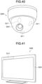
- FIG. 40 is a view for describing an application example of the communication device according to the present embodiment, and illustrates an example of a case where the technology according to the present disclosure is applied to a camera device installed on a lower portion of a drone. Specifically, in a case of a drone flying in a high place, it is preferable to be able to transmit or receive a wireless signal from below in each direction. Therefore, for example, in the example illustrated in FIG.
- the antenna device according to the embodiment of the present disclosure is held so as to be positioned in the vicinity of each of portions that face different directions in an outer surface 5201 of a housing of a camera device 5200 installed on a lower portion of a drone.
- Reference Sign 5211 schematically indicates the antenna device according to the embodiment of the present disclosure.
- the antenna device 5211 may be provided not only in the camera device 5200, but also in various portions of the housing of the drone itself, for example. Also in this case, the antenna device 5211 is preferably provided on, in particular, the lower side of the housing.
- the antenna device 5211 is preferably held in the vicinity of a plurality of partial regions at positions where normal directions are intersect with each other or mutually twisted, among partial regions in the curved surface.
- the camera device 5200 illustrated in FIG. 40 can transmit or receive a wireless signal propagating in a direction that substantially coincides with a normal direction of each partial region.
- FIGS. 41 to 43 are views for describing application examples of the antenna device according to the present embodiment, and each illustrate an example of a case where the antenna device according to the present embodiment is applied to a device other than the communication device such as a so-called smartphone.
- FIG. 41 illustrates an example in which the antenna device according to the present embodiment is provided in a housing of a display device 5300 such as a so-called display.
- Reference Sign 5311 schematically indicates the antenna device according to the embodiment of the present disclosure.
- the antenna device 5311 is arranged so as to be positioned in the vicinity of a front surface 5301 where a display panel is arranged, in the housing of the display device 5300.
- the antenna device 5311 is arranged at a position where the antenna device 5311 does not interfere with each device for displaying an image on the display panel.
- the antenna device 5311 can transmit or receive a wireless signal propagating in a direction that substantially coincides with a normal direction of the front surface 5301.
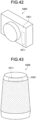
- FIG. 42 illustrates an example in which the antenna device according to the present embodiment is provided in a housing of an image capturing device 5400 such as a so-called digital still camera.
- Reference Sign 5411 schematically indicates the antenna device according to the embodiment of the present disclosure.
- the antenna device 5411 is arranged so as to be positioned at a part of a portion of the housing of the image capturing device 5400 that is different from a portion where a user's hand is put when the user grips the housing of the image capturing device 5400. More specifically, in the example illustrated in FIG.
- the antenna device 5411 is arranged at a position different from a position where a lens is arranged, in a front surface 5401 of the housing of the image capturing device 5400. That is, it is more preferable that the antenna device 5411 is arranged at a position where the antenna device 5411 does not interfere with a component related to image capturing, such as a lens or an image sensor. Thereby, in the example illustrated in FIG. 42 , the antenna device 5411 can transmit or receive a wireless signal propagating in a direction that substantially coincides with a normal direction of the surface 5401.
- FIG. 43 illustrates an example of a case where the antenna device according to the present embodiment is provided in a housing of an acoustic output device 5500 such as a so-called speaker (for example, smart speaker).
- Reference Sign 5511 schematically indicates the antenna device according to the embodiment of the present disclosure.
- the acoustic output device 5500 includes the housing having a substantially cylindrical shape, and the antenna device 5511 is arranged so as to be positioned in the vicinity of a part of a side surface 5501 of the housing.
- the antenna device 5511 is arranged at a position where the antenna device 5511 does not interfere with a component related to output of sound.
- the antenna device 5511 can transmit or receive a wireless signal propagating in a direction that substantially coincides with a normal direction of a portion of the side surface 5501 that is near a portion where the antenna device 5511 is arranged.
- the antenna device includes a substantially-flat-plate-shaped dielectric substrate, a metal base plate, substantially-flat-plate-shaped first and second antenna elements, and first and second feeding portions.
- the metal base plate is arranged on a first surface of the dielectric substrate.
- the first antenna element and the second antenna element are arranged on a second surface of the dielectric substrate that is opposite to the first surface and on an opposite side of the dielectric substrate from the metal base plate, so that a slit is formed.
- the first feeding portion feeds power to the first antenna element.
- the second feeding portion feeds power to the second antenna element.
- a phase difference between feeding signals supplied to the first feeding portion and the second feeding portion, respectively, is approximately 180 degrees.
- the communication device includes the above-described antenna device according to the present embodiment.
- the antenna device according to the embodiment of the present disclosure can further reduce a change in various characteristics when a metal is brought close to the antenna device. Further, with the configuration characteristics described above, the antenna device according to the present embodiment can perform so-called unbalanced power feeding, the degree of freedom in a case of providing the feeding portion in a form in which a radiation pattern is not blocked by the feeding portion (for example, feeding line) is increased, and the antenna device also has a high affinity with a general microstrip line. That is, with the antenna device according to the present embodiment, even in a situation where the antenna device is installed in a limited space inside the housing of the communication device, an influence of proximity to a metal can be further reduced, and power can be fed to the antenna element in a more suitable manner.
Landscapes
- Physics & Mathematics (AREA)
- Electromagnetism (AREA)
- Engineering & Computer Science (AREA)
- Computer Networks & Wireless Communication (AREA)
- Details Of Aerials (AREA)
- Waveguide Aerials (AREA)
Claims (5)
- Antennenvorrichtung (100), umfassend:ein im Wesentlichen flaches, plattenförmiges dielektrisches Substrat (103);eine metallische Grundplatte (101), die auf einer ersten Oberfläche des dielektrischen Substrats angeordnet ist;ein im Wesentlichen flaches, plattenförmiges erstes und zweites Antennenelement (105a, 105b), die auf einer zweiten Oberfläche des dielektrischen Substrats angeordnet sind, die der ersten Oberfläche gegenüberliegt, so dass ein Schlitz (107) ausgebildet wird;einen ersten Einspeisungsabschnitt (109a), der konfiguriert ist, um Strom in das erste Antennenelement einzuspeisen; undeinen zweiten Einspeisungsabschnitt (109b), der konfiguriert ist, um Strom in das zweite Antennenelement einzuspeisen,derart, dass eine Phasendifferenz zwischen Einspeisungssignalen, die dem ersten bzw. dem zweiten Einspeisungsabschnitt zugeführt werden, ungefähr 180 Grad beträgt;wobei eine Strahlungsoberfläche von jedem des ersten und des zweiten Antennenelements eine Form aufweist, die im Wesentlichen die gleiche ist wie ein Quadrat, das eine Seite aufweist, deren Länge im Wesentlichen gleich 1/4 einer Wellenlänge eines zu sendenden oder zu empfangenden drahtlosen Signals ist; undwobei das erste und das zweite Antennenelement derart angeordnet sind, eine Breite des Schlitzes 1/10 oder weniger der Länge der einen Seite der Strahlungsoberfläche beträgt, die eine Form aufweist, die im Wesentlichen die gleiche wie ein Quadrat ist.
- Antennenvorrichtung nach Anspruch 1, wobei das erste und das zweite Antennenelement angeordnet sind, um elektrisch voneinander getrennt zu sein.
- Antennenvorrichtung nach Anspruch 1, wobei der erste und der zweite Einspeisungsabschnitt angeordnet sind, sodass eine erste Richtung, in der sich der Schlitz erstreckt, und eine zweite Richtung von einem der Einspeisungspunkte, die dem ersten bzw. zweiten Einspeisungsabschnitt entsprechen, zu dem anderen Einspeisungspunkt im Wesentlichen orthogonal zueinander sind.
- Antennenvorrichtung nach Anspruch 1, wobei die metallische Grundplatte geformt ist, sodass eine Breite der metallischen Grundplatte in einer Richtung, in der sich der Schlitz erstreckt, größer als die von jedem des ersten und des zweiten Antennenelements ist.
- Antennenvorrichtung nach Anspruch 1, ferner umfassendeine Einspeisungsschaltung, die konfiguriert ist, um das Einspeisungssignal an mindestens einen des ersten Einspeisungsabschnitts und/oder des zweiten Einspeisungsabschnitts zuzuführen,wobei die Einspeisungsschaltung angeordnet ist, um auf einer dem dielektrischen Substrat gegenüberliegenden Seite der metallischen Grundplatte positioniert zu sein.
Applications Claiming Priority (1)
| Application Number | Priority Date | Filing Date | Title |
|---|---|---|---|
| PCT/JP2018/028498 WO2020026312A1 (ja) | 2018-07-30 | 2018-07-30 | アンテナ装置及び通信装置 |
Publications (3)
| Publication Number | Publication Date |
|---|---|
| EP3832800A1 EP3832800A1 (de) | 2021-06-09 |
| EP3832800A4 EP3832800A4 (de) | 2021-08-04 |
| EP3832800B1 true EP3832800B1 (de) | 2024-08-28 |
Family
ID=69231588
Family Applications (1)
| Application Number | Title | Priority Date | Filing Date |
|---|---|---|---|
| EP18928644.6A Active EP3832800B1 (de) | 2018-07-30 | 2018-07-30 | Antennenvorrichtung und kommunikationsvorrichtung |
Country Status (3)
| Country | Link |
|---|---|
| US (1) | US11769943B2 (de) |
| EP (1) | EP3832800B1 (de) |
| WO (1) | WO2020026312A1 (de) |
Families Citing this family (3)
| Publication number | Priority date | Publication date | Assignee | Title |
|---|---|---|---|---|
| CN115313029B (zh) * | 2022-08-24 | 2026-02-06 | Oppo广东移动通信有限公司 | 天线模组、显示屏、设备、参数确定方法以及装置 |
| CN117832834A (zh) * | 2022-09-29 | 2024-04-05 | 华为技术有限公司 | 天线结构及电子设备 |
| CN116721608B (zh) * | 2023-06-13 | 2024-03-08 | 云谷(固安)科技有限公司 | 反射面组件、显示面板和无线通信装置 |
Family Cites Families (12)
| Publication number | Priority date | Publication date | Assignee | Title |
|---|---|---|---|---|
| JPH0993029A (ja) | 1995-09-21 | 1997-04-04 | Matsushita Electric Ind Co Ltd | アンテナ装置 |
| JP2001189615A (ja) | 1999-10-18 | 2001-07-10 | Matsushita Electric Ind Co Ltd | 移動無線用アンテナおよび、それを用いた携帯型無線機 |
| US6549169B1 (en) * | 1999-10-18 | 2003-04-15 | Matsushita Electric Industrial Co., Ltd. | Antenna for mobile wireless communications and portable-type wireless apparatus using the same |
| DE102004054466A1 (de) * | 2004-11-11 | 2006-06-08 | Robert Bosch Gmbh | Radarsystem insbesondere zur Entfernungs- und/oder Geschwindigkeitsmessung |
| JP4557169B2 (ja) | 2005-10-03 | 2010-10-06 | 株式会社デンソー | アンテナ |
| US7868841B2 (en) * | 2007-04-11 | 2011-01-11 | Vubiq Incorporated | Full-wave di-patch antenna |
| JP6387263B6 (ja) | 2014-07-30 | 2018-09-26 | 株式会社Hysエンジニアリングサービス | アンテナ装置 |
| JP6452477B2 (ja) * | 2015-02-06 | 2019-01-16 | 学校法人金沢工業大学 | アンテナ及びそれを用いた通信装置 |
| EP3262711B1 (de) * | 2015-02-26 | 2020-11-18 | The Government of the United States of America as represented by the Secretary of the Navy | Modulare ultrabreitband-planarantennengruppe mit verbesserter bandbreite |
| US10270174B2 (en) * | 2017-07-25 | 2019-04-23 | Apple Inc. | Millimeter wave antennas having cross-shaped resonating elements |
| KR102577295B1 (ko) * | 2018-10-23 | 2023-09-12 | 삼성전자주식회사 | 다중 대역의 신호를 송수신하는 안테나 엘리먼트들이 중첩되어 형성된 안테나 및 이를 포함하는 전자 장치 |
| US11158948B2 (en) * | 2019-03-20 | 2021-10-26 | Samsung Electro-Mechanics Co., Ltd. | Antenna apparatus |
-
2018
- 2018-07-30 EP EP18928644.6A patent/EP3832800B1/de active Active
- 2018-07-30 US US17/262,226 patent/US11769943B2/en active Active
- 2018-07-30 WO PCT/JP2018/028498 patent/WO2020026312A1/ja not_active Ceased
Non-Patent Citations (1)
| Title |
|---|
| ANONYMOUS: "Standard FR4 TG135 Datasheet", 23 August 2022 (2022-08-23), pages 1 - 1, XP055954229, Retrieved from the Internet <URL:http://www.wedirekt.com/web/mandators/media/16_wedirekt/spezifikationen/leiterplatten_daten_downloads/FR4TG135_UK.pdf> [retrieved on 20220823] * |
Also Published As
| Publication number | Publication date |
|---|---|
| WO2020026312A1 (ja) | 2020-02-06 |
| US20210305691A1 (en) | 2021-09-30 |
| US11769943B2 (en) | 2023-09-26 |
| EP3832800A1 (de) | 2021-06-09 |
| EP3832800A4 (de) | 2021-08-04 |
Similar Documents
| Publication | Publication Date | Title |
|---|---|---|
| CN110785893B (zh) | 天线模块和通信装置 | |
| US10957978B2 (en) | Electronic devices having multi-frequency ultra-wideband antennas | |
| CN110970728B (zh) | 具有天线模块隔离结构的电子设备 | |
| US10608344B2 (en) | Electronic device antenna arrays mounted against a dielectric layer | |
| US11552391B2 (en) | Mobile device with multiple-antenna system | |
| JP7228720B2 (ja) | ハウジングアセンブリ、アンテナデバイス及び電子機器 | |
| EP3465823B1 (de) | C-gespeiste, auf einer mehrschichtigen leiterplattenkante gebildete antenne | |
| KR20200036736A (ko) | 통신 및 레인징 능력들을 갖는 전자 디바이스들 | |
| JP6954376B2 (ja) | アンテナアレイおよびアンテナモジュール | |
| DE102020211082A1 (de) | Integrierte millimeterwellen-antennenmodule | |
| US11881630B2 (en) | Beam steering antenna structure and electronic device comprising said structure | |
| DE202016006518U1 (de) | Drahtlos-Lade- und Kommunikationssysteme mit Doppelfrequenz-Patch-Antennen | |
| US20180269585A1 (en) | Hybrid feed technique for planar antenna | |
| CN112234344A (zh) | 天线装置及电子设备 | |
| CN110854548A (zh) | 天线结构及具有该天线结构的无线通信装置 | |
| EP3832800B1 (de) | Antennenvorrichtung und kommunikationsvorrichtung | |
| EP2629366A1 (de) | Antenne und drahtlose kommunikationsvorrichtung | |
| KR20230039534A (ko) | 콤팩트한 초광대역 안테나 모듈들을 갖는 전자 디바이스들 | |
| US12592492B2 (en) | Locating antennas in an apparatus | |
| US20140347247A1 (en) | Antenna device for electronic device | |
| CN112153833A (zh) | 壳体组件、天线装置及电子设备 | |
| KR20050075966A (ko) | 전방향 방사 안테나 | |
| EP3471203B1 (de) | Antenne und mobiles endgerät | |
| CN119181971B (zh) | 天线组件及电子设备 | |
| JPH04196702A (ja) | マイクロストリップパッチ型アレイアンテナ |
Legal Events
| Date | Code | Title | Description |
|---|---|---|---|
| STAA | Information on the status of an ep patent application or granted ep patent |
Free format text: STATUS: THE INTERNATIONAL PUBLICATION HAS BEEN MADE |
|
| PUAI | Public reference made under article 153(3) epc to a published international application that has entered the european phase |
Free format text: ORIGINAL CODE: 0009012 |
|
| STAA | Information on the status of an ep patent application or granted ep patent |
Free format text: STATUS: REQUEST FOR EXAMINATION WAS MADE |
|
| 17P | Request for examination filed |
Effective date: 20210114 |
|
| AK | Designated contracting states |
Kind code of ref document: A1 Designated state(s): AL AT BE BG CH CY CZ DE DK EE ES FI FR GB GR HR HU IE IS IT LI LT LU LV MC MK MT NL NO PL PT RO RS SE SI SK SM TR |
|
| REG | Reference to a national code |
Ref country code: DE Ref legal event code: R079 Ipc: H01Q0001380000 Ref country code: DE Ref legal event code: R079 Ref document number: 602018073823 Country of ref document: DE Free format text: PREVIOUS MAIN CLASS: H01Q0013080000 Ipc: H01Q0001380000 |
|
| RAP3 | Party data changed (applicant data changed or rights of an application transferred) |
Owner name: SONY GROUP CORPORATION |
|
| A4 | Supplementary search report drawn up and despatched |
Effective date: 20210702 |
|
| RIC1 | Information provided on ipc code assigned before grant |
Ipc: H01Q 1/38 20060101AFI20210628BHEP Ipc: H01Q 9/06 20060101ALI20210628BHEP Ipc: H01Q 19/10 20060101ALI20210628BHEP Ipc: H01Q 1/24 20060101ALI20210628BHEP |
|
| DAV | Request for validation of the european patent (deleted) | ||
| DAX | Request for extension of the european patent (deleted) | ||
| STAA | Information on the status of an ep patent application or granted ep patent |
Free format text: STATUS: EXAMINATION IS IN PROGRESS |
|
| 17Q | First examination report despatched |
Effective date: 20220831 |
|
| GRAP | Despatch of communication of intention to grant a patent |
Free format text: ORIGINAL CODE: EPIDOSNIGR1 |
|
| STAA | Information on the status of an ep patent application or granted ep patent |
Free format text: STATUS: GRANT OF PATENT IS INTENDED |
|
| INTG | Intention to grant announced |
Effective date: 20240306 |
|
| GRAS | Grant fee paid |
Free format text: ORIGINAL CODE: EPIDOSNIGR3 |
|
| P01 | Opt-out of the competence of the unified patent court (upc) registered |
Free format text: CASE NUMBER: APP_33809/2024 Effective date: 20240606 |
|
| GRAA | (expected) grant |
Free format text: ORIGINAL CODE: 0009210 |
|
| STAA | Information on the status of an ep patent application or granted ep patent |
Free format text: STATUS: THE PATENT HAS BEEN GRANTED |
|
| AK | Designated contracting states |
Kind code of ref document: B1 Designated state(s): AL AT BE BG CH CY CZ DE DK EE ES FI FR GB GR HR HU IE IS IT LI LT LU LV MC MK MT NL NO PL PT RO RS SE SI SK SM TR |
|
| REG | Reference to a national code |
Ref country code: GB Ref legal event code: FG4D |
|
| REG | Reference to a national code |
Ref country code: CH Ref legal event code: EP |
|
| REG | Reference to a national code |
Ref country code: DE Ref legal event code: R096 Ref document number: 602018073823 Country of ref document: DE |
|
| REG | Reference to a national code |
Ref country code: IE Ref legal event code: FG4D |
|
| REG | Reference to a national code |
Ref country code: LT Ref legal event code: MG9D |
|
| PG25 | Lapsed in a contracting state [announced via postgrant information from national office to epo] |
Ref country code: NO Free format text: LAPSE BECAUSE OF FAILURE TO SUBMIT A TRANSLATION OF THE DESCRIPTION OR TO PAY THE FEE WITHIN THE PRESCRIBED TIME-LIMIT Effective date: 20241128 |
|
| REG | Reference to a national code |
Ref country code: AT Ref legal event code: MK05 Ref document number: 1719019 Country of ref document: AT Kind code of ref document: T Effective date: 20240828 |
|
| PG25 | Lapsed in a contracting state [announced via postgrant information from national office to epo] |
Ref country code: NL Free format text: LAPSE BECAUSE OF FAILURE TO SUBMIT A TRANSLATION OF THE DESCRIPTION OR TO PAY THE FEE WITHIN THE PRESCRIBED TIME-LIMIT Effective date: 20240828 Ref country code: FI Free format text: LAPSE BECAUSE OF FAILURE TO SUBMIT A TRANSLATION OF THE DESCRIPTION OR TO PAY THE FEE WITHIN THE PRESCRIBED TIME-LIMIT Effective date: 20240828 Ref country code: PL Free format text: LAPSE BECAUSE OF FAILURE TO SUBMIT A TRANSLATION OF THE DESCRIPTION OR TO PAY THE FEE WITHIN THE PRESCRIBED TIME-LIMIT Effective date: 20240828 Ref country code: GR Free format text: LAPSE BECAUSE OF FAILURE TO SUBMIT A TRANSLATION OF THE DESCRIPTION OR TO PAY THE FEE WITHIN THE PRESCRIBED TIME-LIMIT Effective date: 20241129 Ref country code: PT Free format text: LAPSE BECAUSE OF FAILURE TO SUBMIT A TRANSLATION OF THE DESCRIPTION OR TO PAY THE FEE WITHIN THE PRESCRIBED TIME-LIMIT Effective date: 20241230 |
|
| PG25 | Lapsed in a contracting state [announced via postgrant information from national office to epo] |
Ref country code: BG Free format text: LAPSE BECAUSE OF FAILURE TO SUBMIT A TRANSLATION OF THE DESCRIPTION OR TO PAY THE FEE WITHIN THE PRESCRIBED TIME-LIMIT Effective date: 20240828 |
|
| PG25 | Lapsed in a contracting state [announced via postgrant information from national office to epo] |
Ref country code: LV Free format text: LAPSE BECAUSE OF FAILURE TO SUBMIT A TRANSLATION OF THE DESCRIPTION OR TO PAY THE FEE WITHIN THE PRESCRIBED TIME-LIMIT Effective date: 20240828 |
|
| REG | Reference to a national code |
Ref country code: NL Ref legal event code: MP Effective date: 20240828 |
|
| PG25 | Lapsed in a contracting state [announced via postgrant information from national office to epo] |
Ref country code: IS Free format text: LAPSE BECAUSE OF FAILURE TO SUBMIT A TRANSLATION OF THE DESCRIPTION OR TO PAY THE FEE WITHIN THE PRESCRIBED TIME-LIMIT Effective date: 20241228 Ref country code: AT Free format text: LAPSE BECAUSE OF FAILURE TO SUBMIT A TRANSLATION OF THE DESCRIPTION OR TO PAY THE FEE WITHIN THE PRESCRIBED TIME-LIMIT Effective date: 20240828 |
|
| PG25 | Lapsed in a contracting state [announced via postgrant information from national office to epo] |
Ref country code: HR Free format text: LAPSE BECAUSE OF FAILURE TO SUBMIT A TRANSLATION OF THE DESCRIPTION OR TO PAY THE FEE WITHIN THE PRESCRIBED TIME-LIMIT Effective date: 20240828 |
|
| PG25 | Lapsed in a contracting state [announced via postgrant information from national office to epo] |
Ref country code: RS Free format text: LAPSE BECAUSE OF FAILURE TO SUBMIT A TRANSLATION OF THE DESCRIPTION OR TO PAY THE FEE WITHIN THE PRESCRIBED TIME-LIMIT Effective date: 20241128 Ref country code: ES Free format text: LAPSE BECAUSE OF FAILURE TO SUBMIT A TRANSLATION OF THE DESCRIPTION OR TO PAY THE FEE WITHIN THE PRESCRIBED TIME-LIMIT Effective date: 20240828 |
|
| PG25 | Lapsed in a contracting state [announced via postgrant information from national office to epo] |
Ref country code: RS Free format text: LAPSE BECAUSE OF FAILURE TO SUBMIT A TRANSLATION OF THE DESCRIPTION OR TO PAY THE FEE WITHIN THE PRESCRIBED TIME-LIMIT Effective date: 20241128 Ref country code: PT Free format text: LAPSE BECAUSE OF FAILURE TO SUBMIT A TRANSLATION OF THE DESCRIPTION OR TO PAY THE FEE WITHIN THE PRESCRIBED TIME-LIMIT Effective date: 20241230 Ref country code: PL Free format text: LAPSE BECAUSE OF FAILURE TO SUBMIT A TRANSLATION OF THE DESCRIPTION OR TO PAY THE FEE WITHIN THE PRESCRIBED TIME-LIMIT Effective date: 20240828 Ref country code: NO Free format text: LAPSE BECAUSE OF FAILURE TO SUBMIT A TRANSLATION OF THE DESCRIPTION OR TO PAY THE FEE WITHIN THE PRESCRIBED TIME-LIMIT Effective date: 20241128 Ref country code: NL Free format text: LAPSE BECAUSE OF FAILURE TO SUBMIT A TRANSLATION OF THE DESCRIPTION OR TO PAY THE FEE WITHIN THE PRESCRIBED TIME-LIMIT Effective date: 20240828 Ref country code: LV Free format text: LAPSE BECAUSE OF FAILURE TO SUBMIT A TRANSLATION OF THE DESCRIPTION OR TO PAY THE FEE WITHIN THE PRESCRIBED TIME-LIMIT Effective date: 20240828 Ref country code: IS Free format text: LAPSE BECAUSE OF FAILURE TO SUBMIT A TRANSLATION OF THE DESCRIPTION OR TO PAY THE FEE WITHIN THE PRESCRIBED TIME-LIMIT Effective date: 20241228 Ref country code: HR Free format text: LAPSE BECAUSE OF FAILURE TO SUBMIT A TRANSLATION OF THE DESCRIPTION OR TO PAY THE FEE WITHIN THE PRESCRIBED TIME-LIMIT Effective date: 20240828 Ref country code: GR Free format text: LAPSE BECAUSE OF FAILURE TO SUBMIT A TRANSLATION OF THE DESCRIPTION OR TO PAY THE FEE WITHIN THE PRESCRIBED TIME-LIMIT Effective date: 20241129 Ref country code: FI Free format text: LAPSE BECAUSE OF FAILURE TO SUBMIT A TRANSLATION OF THE DESCRIPTION OR TO PAY THE FEE WITHIN THE PRESCRIBED TIME-LIMIT Effective date: 20240828 Ref country code: ES Free format text: LAPSE BECAUSE OF FAILURE TO SUBMIT A TRANSLATION OF THE DESCRIPTION OR TO PAY THE FEE WITHIN THE PRESCRIBED TIME-LIMIT Effective date: 20240828 Ref country code: BG Free format text: LAPSE BECAUSE OF FAILURE TO SUBMIT A TRANSLATION OF THE DESCRIPTION OR TO PAY THE FEE WITHIN THE PRESCRIBED TIME-LIMIT Effective date: 20240828 Ref country code: AT Free format text: LAPSE BECAUSE OF FAILURE TO SUBMIT A TRANSLATION OF THE DESCRIPTION OR TO PAY THE FEE WITHIN THE PRESCRIBED TIME-LIMIT Effective date: 20240828 |
|
| PG25 | Lapsed in a contracting state [announced via postgrant information from national office to epo] |
Ref country code: RO Free format text: LAPSE BECAUSE OF FAILURE TO SUBMIT A TRANSLATION OF THE DESCRIPTION OR TO PAY THE FEE WITHIN THE PRESCRIBED TIME-LIMIT Effective date: 20240828 Ref country code: DK Free format text: LAPSE BECAUSE OF FAILURE TO SUBMIT A TRANSLATION OF THE DESCRIPTION OR TO PAY THE FEE WITHIN THE PRESCRIBED TIME-LIMIT Effective date: 20240828 Ref country code: SM Free format text: LAPSE BECAUSE OF FAILURE TO SUBMIT A TRANSLATION OF THE DESCRIPTION OR TO PAY THE FEE WITHIN THE PRESCRIBED TIME-LIMIT Effective date: 20240828 |
|
| PG25 | Lapsed in a contracting state [announced via postgrant information from national office to epo] |
Ref country code: EE Free format text: LAPSE BECAUSE OF FAILURE TO SUBMIT A TRANSLATION OF THE DESCRIPTION OR TO PAY THE FEE WITHIN THE PRESCRIBED TIME-LIMIT Effective date: 20240828 |
|
| PG25 | Lapsed in a contracting state [announced via postgrant information from national office to epo] |
Ref country code: CZ Free format text: LAPSE BECAUSE OF FAILURE TO SUBMIT A TRANSLATION OF THE DESCRIPTION OR TO PAY THE FEE WITHIN THE PRESCRIBED TIME-LIMIT Effective date: 20240828 |
|
| PG25 | Lapsed in a contracting state [announced via postgrant information from national office to epo] |
Ref country code: IT Free format text: LAPSE BECAUSE OF FAILURE TO SUBMIT A TRANSLATION OF THE DESCRIPTION OR TO PAY THE FEE WITHIN THE PRESCRIBED TIME-LIMIT Effective date: 20240828 Ref country code: SK Free format text: LAPSE BECAUSE OF FAILURE TO SUBMIT A TRANSLATION OF THE DESCRIPTION OR TO PAY THE FEE WITHIN THE PRESCRIBED TIME-LIMIT Effective date: 20240828 |
|
| REG | Reference to a national code |
Ref country code: DE Ref legal event code: R097 Ref document number: 602018073823 Country of ref document: DE |
|
| PLBE | No opposition filed within time limit |
Free format text: ORIGINAL CODE: 0009261 |
|
| STAA | Information on the status of an ep patent application or granted ep patent |
Free format text: STATUS: NO OPPOSITION FILED WITHIN TIME LIMIT |
|
| 26N | No opposition filed |
Effective date: 20250530 |
|
| PG25 | Lapsed in a contracting state [announced via postgrant information from national office to epo] |
Ref country code: SE Free format text: LAPSE BECAUSE OF FAILURE TO SUBMIT A TRANSLATION OF THE DESCRIPTION OR TO PAY THE FEE WITHIN THE PRESCRIBED TIME-LIMIT Effective date: 20240828 |
|
| PGFP | Annual fee paid to national office [announced via postgrant information from national office to epo] |
Ref country code: DE Payment date: 20250620 Year of fee payment: 8 |
|
| REG | Reference to a national code |
Ref country code: CH Ref legal event code: H13 Free format text: ST27 STATUS EVENT CODE: U-0-0-H10-H13 (AS PROVIDED BY THE NATIONAL OFFICE) Effective date: 20260224 |
|
| PG25 | Lapsed in a contracting state [announced via postgrant information from national office to epo] |
Ref country code: LU Free format text: LAPSE BECAUSE OF NON-PAYMENT OF DUE FEES Effective date: 20250730 |
|
| GBPC | Gb: european patent ceased through non-payment of renewal fee |
Effective date: 20250730 |
|
| REG | Reference to a national code |
Ref country code: BE Ref legal event code: MM Effective date: 20250731 |
|
| PG25 | Lapsed in a contracting state [announced via postgrant information from national office to epo] |
Ref country code: GB Free format text: LAPSE BECAUSE OF NON-PAYMENT OF DUE FEES Effective date: 20250730 |
|
| PG25 | Lapsed in a contracting state [announced via postgrant information from national office to epo] |
Ref country code: BE Free format text: LAPSE BECAUSE OF NON-PAYMENT OF DUE FEES Effective date: 20250731 |
|
| PG25 | Lapsed in a contracting state [announced via postgrant information from national office to epo] |
Ref country code: FR Free format text: LAPSE BECAUSE OF NON-PAYMENT OF DUE FEES Effective date: 20250731 |
|
| PG25 | Lapsed in a contracting state [announced via postgrant information from national office to epo] |
Ref country code: CH Free format text: LAPSE BECAUSE OF NON-PAYMENT OF DUE FEES Effective date: 20250731 |