EP3834403B1 - Dispositif électronique comprenant une antenne connectée à une feuille conductrice d'un écran d'affichage - Google Patents
Dispositif électronique comprenant une antenne connectée à une feuille conductrice d'un écran d'affichage Download PDFInfo
- Publication number
- EP3834403B1 EP3834403B1 EP19876180.1A EP19876180A EP3834403B1 EP 3834403 B1 EP3834403 B1 EP 3834403B1 EP 19876180 A EP19876180 A EP 19876180A EP 3834403 B1 EP3834403 B1 EP 3834403B1
- Authority
- EP
- European Patent Office
- Prior art keywords
- pcb
- electronic device
- ground
- conductive sheet
- fpcb
- Prior art date
- Legal status (The legal status is an assumption and is not a legal conclusion. Google has not performed a legal analysis and makes no representation as to the accuracy of the status listed.)
- Active
Links
Images




Classifications
-
- H—ELECTRICITY
- H04—ELECTRIC COMMUNICATION TECHNIQUE
- H04M—TELEPHONIC COMMUNICATION
- H04M1/00—Substation equipment, e.g. for use by subscribers
- H04M1/02—Constructional features of telephone sets
- H04M1/0202—Portable telephone sets, e.g. cordless phones, mobile phones or bar type handsets
- H04M1/0249—Details of the mechanical connection between the housing parts or relating to the method of assembly
-
- H—ELECTRICITY
- H01—ELECTRIC ELEMENTS
- H01Q—ANTENNAS, i.e. RADIO AERIALS
- H01Q1/00—Details of, or arrangements associated with, antennas
- H01Q1/12—Supports; Mounting means
- H01Q1/22—Supports; Mounting means by structural association with other equipment or articles
- H01Q1/24—Supports; Mounting means by structural association with other equipment or articles with receiving set
- H01Q1/241—Supports; Mounting means by structural association with other equipment or articles with receiving set used in mobile communications, e.g. GSM
- H01Q1/242—Supports; Mounting means by structural association with other equipment or articles with receiving set used in mobile communications, e.g. GSM specially adapted for hand-held use
- H01Q1/243—Supports; Mounting means by structural association with other equipment or articles with receiving set used in mobile communications, e.g. GSM specially adapted for hand-held use with built-in antennas
-
- H—ELECTRICITY
- H01—ELECTRIC ELEMENTS
- H01Q—ANTENNAS, i.e. RADIO AERIALS
- H01Q1/00—Details of, or arrangements associated with, antennas
- H01Q1/36—Structural form of radiating elements, e.g. cone, spiral, umbrella; Particular materials used therewith
- H01Q1/38—Structural form of radiating elements, e.g. cone, spiral, umbrella; Particular materials used therewith formed by a conductive layer on an insulating support
-
- H—ELECTRICITY
- H01—ELECTRIC ELEMENTS
- H01Q—ANTENNAS, i.e. RADIO AERIALS
- H01Q1/00—Details of, or arrangements associated with, antennas
- H01Q1/48—Earthing means; Earth screens; Counterpoises
-
- H—ELECTRICITY
- H01—ELECTRIC ELEMENTS
- H01Q—ANTENNAS, i.e. RADIO AERIALS
- H01Q1/00—Details of, or arrangements associated with, antennas
- H01Q1/52—Means for reducing coupling between antennas; Means for reducing coupling between an antenna and another structure
-
- H—ELECTRICITY
- H04—ELECTRIC COMMUNICATION TECHNIQUE
- H04M—TELEPHONIC COMMUNICATION
- H04M1/00—Substation equipment, e.g. for use by subscribers
- H04M1/02—Constructional features of telephone sets
- H04M1/0202—Portable telephone sets, e.g. cordless phones, mobile phones or bar type handsets
- H04M1/026—Details of the structure or mounting of specific components
-
- H—ELECTRICITY
- H04—ELECTRIC COMMUNICATION TECHNIQUE
- H04M—TELEPHONIC COMMUNICATION
- H04M1/00—Substation equipment, e.g. for use by subscribers
- H04M1/02—Constructional features of telephone sets
- H04M1/0202—Portable telephone sets, e.g. cordless phones, mobile phones or bar type handsets
- H04M1/026—Details of the structure or mounting of specific components
- H04M1/0277—Details of the structure or mounting of specific components for a printed circuit board assembly
-
- H—ELECTRICITY
- H05—ELECTRIC TECHNIQUES NOT OTHERWISE PROVIDED FOR
- H05K—PRINTED CIRCUITS; CASINGS OR CONSTRUCTIONAL DETAILS OF ELECTRIC APPARATUS; MANUFACTURE OF ASSEMBLAGES OF ELECTRICAL COMPONENTS
- H05K1/00—Printed circuits
- H05K1/02—Details
- H05K1/14—Structural association of two or more printed circuits
- H05K1/147—Structural association of two or more printed circuits at least one of the printed circuits being bent or folded, e.g. by using a flexible printed circuit
-
- H—ELECTRICITY
- H05—ELECTRIC TECHNIQUES NOT OTHERWISE PROVIDED FOR
- H05K—PRINTED CIRCUITS; CASINGS OR CONSTRUCTIONAL DETAILS OF ELECTRIC APPARATUS; MANUFACTURE OF ASSEMBLAGES OF ELECTRICAL COMPONENTS
- H05K5/00—Casings, cabinets or drawers for electric apparatus
- H05K5/0017—Casings, cabinets or drawers for electric apparatus with operator interface units
-
- H—ELECTRICITY
- H05—ELECTRIC TECHNIQUES NOT OTHERWISE PROVIDED FOR
- H05K—PRINTED CIRCUITS; CASINGS OR CONSTRUCTIONAL DETAILS OF ELECTRIC APPARATUS; MANUFACTURE OF ASSEMBLAGES OF ELECTRICAL COMPONENTS
- H05K5/00—Casings, cabinets or drawers for electric apparatus
- H05K5/02—Details
- H05K5/03—Covers
-
- H—ELECTRICITY
- H05—ELECTRIC TECHNIQUES NOT OTHERWISE PROVIDED FOR
- H05K—PRINTED CIRCUITS; CASINGS OR CONSTRUCTIONAL DETAILS OF ELECTRIC APPARATUS; MANUFACTURE OF ASSEMBLAGES OF ELECTRICAL COMPONENTS
- H05K1/00—Printed circuits
- H05K1/02—Details
- H05K1/0213—Electrical arrangements not otherwise provided for
- H05K1/0237—High frequency adaptations
- H05K1/0243—Printed circuits associated with mounted high frequency components
-
- H—ELECTRICITY
- H05—ELECTRIC TECHNIQUES NOT OTHERWISE PROVIDED FOR
- H05K—PRINTED CIRCUITS; CASINGS OR CONSTRUCTIONAL DETAILS OF ELECTRIC APPARATUS; MANUFACTURE OF ASSEMBLAGES OF ELECTRICAL COMPONENTS
- H05K1/00—Printed circuits
- H05K1/18—Printed circuits structurally associated with non-printed electric components
- H05K1/189—Printed circuits structurally associated with non-printed electric components characterised by the use of flexible or folded printed circuits
-
- H—ELECTRICITY
- H05—ELECTRIC TECHNIQUES NOT OTHERWISE PROVIDED FOR
- H05K—PRINTED CIRCUITS; CASINGS OR CONSTRUCTIONAL DETAILS OF ELECTRIC APPARATUS; MANUFACTURE OF ASSEMBLAGES OF ELECTRICAL COMPONENTS
- H05K2201/00—Indexing scheme relating to printed circuits covered by H05K1/00
- H05K2201/05—Flexible printed circuits [FPCs]
- H05K2201/056—Folded around rigid support or component
-
- H—ELECTRICITY
- H05—ELECTRIC TECHNIQUES NOT OTHERWISE PROVIDED FOR
- H05K—PRINTED CIRCUITS; CASINGS OR CONSTRUCTIONAL DETAILS OF ELECTRIC APPARATUS; MANUFACTURE OF ASSEMBLAGES OF ELECTRICAL COMPONENTS
- H05K2201/00—Indexing scheme relating to printed circuits covered by H05K1/00
- H05K2201/10—Details of components or other objects attached to or integrated in a printed circuit board
- H05K2201/10007—Types of components
- H05K2201/10098—Components for radio transmission, e.g. radio frequency identification [RFID] tag, printed or non-printed antennas
-
- H—ELECTRICITY
- H05—ELECTRIC TECHNIQUES NOT OTHERWISE PROVIDED FOR
- H05K—PRINTED CIRCUITS; CASINGS OR CONSTRUCTIONAL DETAILS OF ELECTRIC APPARATUS; MANUFACTURE OF ASSEMBLAGES OF ELECTRICAL COMPONENTS
- H05K2201/00—Indexing scheme relating to printed circuits covered by H05K1/00
- H05K2201/10—Details of components or other objects attached to or integrated in a printed circuit board
- H05K2201/10007—Types of components
- H05K2201/10128—Display
Definitions
- the disclosure relates to connecting an antenna included in an electronic device with a conductive sheet of a display panel.
- the electronic device including an antenna has been extensively spread.
- the electronic device may transmit and/or receive a radio frequency (RF) signal including a voice signal or data (e.g., a message, a photo, a moving picture, a music file, or the like) using the antenna.
- RF radio frequency
- the electronic device may include a display to display an image.
- the display includes a conductive sheet to block noise from being introduced into an electrical circuit constituting the display.
- an electronic device such as a smartphone
- the display panel is significantly close to a side member of the electronic device, even the conductive sheet is significantly close to the side member.
- an electronic device having a metal side member utilizes a portion of the metal side member as an antenna.
- WO 2018/052188 Al and US 2018/017999 Al disclose an electronic device with a conductive sheet under a display, a PCB, and an FPCB passing through a via hole or recess in a support structure, the support structure sandwiched between the display and conductive sheet on one side and the PCB on its other side.
- the distances between the side member and a feeder of the antenna, and the display panel may be decreased.
- the conductive sheet of the display panel is a floating ground, the radiation efficiency of the antenna may be lowered.
- a pressed phenomenon may occur in an area of the display panel having the connection part disposed therein.
- the pixel on the display panel may be degraded or a dead pixel recognized as a dark point may be formed due to the pressure applied to the display panel, and a leakage current may be caused.
- an example aspect of the disclosure is to provide an electronic device according to the appended claims including an antenna connected with a conductive sheet of a display panel, in which the conductive sheet of the display panel is connected with the ground of a PCB to function as the ground of the antenna while preventing and/or reducing instances of pixels on the display panel being degraded.
- an electronic device may include glass comprising a front surface of the electronic device, a display panel disposed under the glass, a conductive sheet attached to the display panel or integrated into the display panel, a support including a side surface of the electronic device and a mounting space for parts, wherein a first portion of the support includes a metal portion configured as a radiator, and insulation portions disposed at opposite ends of the metal portion, and a second portion of the support includes at least one via hole or recess, a printed circuit board (PCB) including a ground, a wireless communication circuit disposed on the PCB, at least one processor operatively connected with the wireless communication circuit, a flexible PCB (FPCB) electrically connected with the conductive sheet and configured to operatively connect the display panel with the at least one processor, and a cover comprising a rear surface of the electronic device.
- PCB printed circuit board
- the glass, the display panel, and the conductive sheet may be seated on a first surface of the second portion of the support.
- the PCB and the cover of the electronic device may be seated on a second surface of the second portion of the support.
- the second portion of the support may electrically connect the support with a ground of the PCB by making contact with one of conductive contacts of the PCB on at least one point.
- the FPCB may include a first path extending from the first surface to the second surface through the at least one via hole or recess of the support.
- the first path of the FPCB extending to the second surface may electrically connect the conductive sheet with the ground of the PCB.
- the conductive sheet may be electrically connected with the metal portion of the support through a selection part comprising a selective connector.
- the wireless communication circuit may be configured to receive a signal having a specific frequency band based on an electrical path including the wireless communication circuit, the metal portion of the support, the selection part, and the conductive sheet.
- an electronic device includes glass comprising a front surface of the electronic device, a display panel disposed under the glass, a conductive sheet attached to the display panel or integrated with the display panel, a housing including a side portion comprising a side surface of the electronic device and a rear plate comprising a rear surface of the electronic device, wherein the side portion includes a metal portion configured to function as a radiator, and an insulation portion which separates the metal portion from a remaining portion of the housing, a PCB including a ground, a support configured to separate the glass, the display panel, and the conductive sheet from the PCB, and the support including at least one via hole or recess, wireless communication circuitry disposed on the PCB, at least one processor operatively connected with the wireless communication circuitry, and an FPCB electrically connected with the conductive sheet configured to operatively connect the display panel with the at least one processor.
- the glass, the display panel, and the conductive sheet are seated on a first surface of the support, the PCB is disposed on a second surface of the support, and the rear plate is configured to electrically connect the housing with the ground of the PCB by making contact with one of conductive contacts of the PCB on at least one point, the FPCB having a first path extending from the first surface to the second surface through the at least one via hole or recess of the support, the first path of the FPCB extending to the second surface electrically connecting the conductive sheet with the ground of the PCB, the conductive sheet is electrically connected with the metal portion of the side portion through a selection part comprising a selective connector, and the wireless communication circuitry is configured to receive a signal having a specific frequency band based on an electrical path formed by the wireless communication circuitry, the metal portion of the side portion, the selection part, and the conductive sheet.
- an electronic device may include a housing including an antenna radiator, a display panel disposed inside the housing, a conductive sheet attached to the display panel or integrated with the display panel, a PCB including a ground, wireless communication circuitry disposed on the PCB configured to feed power to the antenna radiator, and at least one processor operatively connected with the wireless communication circuitry.
- the conductive sheet may be electrically connected with the ground of the PCB, and the wireless communication circuitry may be configured to receive a signal having a specific frequency band based on an electrical path between the wireless communication circuitry and the antenna radiator, or between the antenna radiator and the conductive sheet.
- the conductive sheet of the display panel may be utilized as a portion of the ground of the antenna to improve the radiation performance of the antenna.
- the display panel is not pressed due to the supporting member and/or the connector on the PCB, thereby preventing and/or reducing the pixels on the display panel from being degraded.
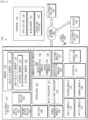
- Fig. 1 is a block diagram illustrating an electronic device 101 in a network environment 100 according to various embodiments.
- the electronic device 101 in the network environment 100 may communicate with an electronic device 102 via a first network 198 (e.g., a short-range wireless communication network), or an electronic device 104 or a server 108 via a second network 199 (e.g., a long-range wireless communication network).
- the electronic device 101 may communicate with the electronic device 104 via the server 108.
- the processor 120 may execute, for example, software (e.g., a program 140) to control at least one other component (e.g., a hardware or software component) of the electronic device 101 coupled with the processor 120, and may perform various data processing or computation. According to an example embodiment, as at least part of the data processing or computation, the processor 120 may load a command or data received from another component (e.g., the sensor module 176 or the communication module 190) in volatile memory 132, process the command or the data stored in the volatile memory 132, and store resulting data in non-volatile memory 134.
- software e.g., a program 140
- the processor 120 may load a command or data received from another component (e.g., the sensor module 176 or the communication module 190) in volatile memory 132, process the command or the data stored in the volatile memory 132, and store resulting data in non-volatile memory 134.
- the processor 120 may include a main processor 121 (e.g., a central processing unit (CPU) or an application processor (AP)), and an auxiliary processor 123 (e.g., a graphics processing unit (GPU), an image signal processor (ISP), a sensor hub processor, or a communication processor (CP)) that is operable independently from, or in conjunction with, the main processor 121.
- auxiliary processor 123 may be adapted to consume less power than the main processor 121, or to be specific to a specified function.
- the auxiliary processor 123 may be implemented as separate from, or as part of the main processor 121.
- the sound output device 155 may output sound signals to the outside of the electronic device 101.
- the sound output device 155 may include, for example, a speaker or a receiver.
- the speaker may be used for general purposes, such as playing multimedia or playing record, and the receiver may be used for an incoming calls. According to an embodiment, the receiver may be implemented as separate from, or as part of the speaker.
- the display device 160 may visually provide information to the outside (e.g., a user) of the electronic device 101.
- the display device 160 may include, for example, a display, a hologram device, or a projector and control circuitry to control a corresponding one of the display, hologram device, and projector.
- the display device 160 may include touch circuitry adapted to detect a touch, or sensor circuitry (e.g., a pressure sensor) adapted to measure the intensity of force incurred by the touch.
- the audio module 170 may convert a sound into an electrical signal and vice versa. According to an embodiment, the audio module 170 may obtain the sound via the input device 150, or output the sound via the sound output device 155 or a headphone of an external electronic device (e.g., an electronic device 102) directly (e.g., wiredly) or wirelessly coupled with the electronic device 101.
- an external electronic device e.g., an electronic device 102
- directly e.g., wiredly
- wirelessly e.g., wirelessly
- the sensor module 176 may detect an operational state (e.g., power or temperature) of the electronic device 101 or an environmental state (e.g., a state of a user) external to the electronic device 101, and then generate an electrical signal or data value corresponding to the detected state.
- the sensor module 176 may include, for example, a gesture sensor, a gyro sensor, an atmospheric pressure sensor, a magnetic sensor, an acceleration sensor, a grip sensor, a proximity sensor, a color sensor, an infrared (IR) sensor, a biometric sensor, a temperature sensor, a humidity sensor, or an illuminance sensor.
- the interface 177 may support one or more specified protocols to be used for the electronic device 101 to be coupled with the external electronic device (e.g., the electronic device 102) directly (e.g., wiredly) or wirelessly.
- the interface 177 may include, for example, a high definition multimedia interface (HDMI), a universal serial bus (USB) interface, a secure digital (SD) card interface, or an audio interface.
- HDMI high definition multimedia interface
- USB universal serial bus
- SD secure digital
- a connecting terminal 178 may include a connector via which the electronic device 101 may be physically connected with the external electronic device (e.g., the electronic device 102).
- the connecting terminal 178 may include, for example, a HDMI connector, a USB connector, a SD card connector, or an audio connector (e.g., a headphone connector).
- the haptic module 179 may convert an electrical signal into a mechanical stimulus (e.g., a vibration or a movement) or electrical stimulus which may be recognized by a user via his tactile sensation or kinesthetic sensation.
- the haptic module 179 may include, for example, a motor, a piezoelectric element, or an electric stimulator.
- the camera module 180 may capture a still image or moving images.
- the camera module 180 may include one or more lenses, image sensors, image signal processors, or flashes.
- the power management module 188 may manage power supplied to the electronic device 101.
- the power management module 188 may be implemented as at least part of, for example, a power management integrated circuit (PMIC).
- PMIC power management integrated circuit
- the battery 189 may supply power to at least one component of the electronic device 101.
- the battery 189 may include, for example, a primary cell which is not rechargeable, a secondary cell which is rechargeable, or a fuel cell.
- the communication module 190 may support establishing a direct (e.g., wired) communication channel or a wireless communication channel between the electronic device 101 and the external electronic device (e.g., the electronic device 102, the electronic device 104, or the server 108) and performing communication via the established communication channel.
- the communication module 190 may include one or more communication processors that are operable independently from the processor 120 (e.g., the application processor (AP)) and supports a direct (e.g., wired) communication or a wireless communication.
- AP application processor
- the communication module 190 may include a wireless communication module 192 (e.g., a cellular communication module, a short-range wireless communication module, or a global navigation satellite system (GNSS) communication module) or a wired communication module 194 (e.g., a local area network (LAN) communication module or a power line communication (PLC) module).
- a wireless communication module 192 e.g., a cellular communication module, a short-range wireless communication module, or a global navigation satellite system (GNSS) communication module
- GNSS global navigation satellite system
- wired communication module 194 e.g., a local area network (LAN) communication module or a power line communication (PLC) module.
- LAN local area network
- PLC power line communication
- a corresponding one of these communication modules may communicate with the external electronic device via the first network 198 (e.g., a short-range communication network, such as Bluetooth , wireless-fidelity (Wi-Fi) direct, or infrared data association (IrDA)) or the second network 199 (e.g., a long-range communication network, such as a cellular network, the Internet, or a computer network (e.g., LAN or wide area network (WAN)).
- the first network 198 e.g., a short-range communication network, such as Bluetooth , wireless-fidelity (Wi-Fi) direct, or infrared data association (IrDA)
- the second network 199 e.g., a long-range communication network, such as a cellular network, the Internet, or a computer network (e.g., LAN or wide area network (WAN)
- These various types of communication modules may be implemented as a single component (e.g., a single chip), or may be implemented as multi components (e.
- the wireless communication module 192 may identify and authenticate the electronic device 101 in a communication network, such as the first network 198 or the second network 199, using subscriber information (e.g., international mobile subscriber identity (IMSI)) stored in the subscriber identification module 196.
- subscriber information e.g., international mobile subscriber identity (IMSI)
- the antenna module 197 may transmit or receive a signal or power to or from the outside (e.g., the external electronic device) of the electronic device 101.
- the antenna module 197 may include an antenna including a radiating element composed of a conductive material or a conductive pattern formed in or on a substrate (e.g., PCB).
- the antenna module 197 may include a plurality of antennas. In such a case, at least one antenna appropriate for a communication scheme used in the communication network, such as the first network 198 or the second network 199, may be selected, for example, by the communication module 190 (e.g., the wireless communication module 192) from the plurality of antennas.
- the signal or the power may then be transmitted or received between the communication module 190 and the external electronic device via the selected at least one antenna.
- another component e.g., a radio frequency integrated circuit (RFIC)
- RFIC radio frequency integrated circuit
- At least some of the above-described components may be coupled mutually and communicate signals (e.g., commands or data) therebetween via an inter-peripheral communication scheme (e.g., a bus, general purpose input and output (GPIO), serial peripheral interface (SPI), or mobile industry processor interface (MIPI)).
- an inter-peripheral communication scheme e.g., a bus, general purpose input and output (GPIO), serial peripheral interface (SPI), or mobile industry processor interface (MIPI)
- commands or data may be transmitted or received between the electronic device 101 and the external electronic device 104 via the server 108 coupled with the second network 199.
- Each of the electronic devices 102 and 104 may be a device of a same type as, or a different type, from the electronic device 101.
- all or some of operations to be executed at the electronic device 101 may be executed at one or more of the external electronic devices 102, 104, or 108. For example, if the electronic device 101 should perform a function or a service automatically, or in response to a request from a user or another device, the electronic device 101, instead of, or in addition to, executing the function or the service, may request the one or more external electronic devices to perform at least part of the function or the service.
- the one or more external electronic devices receiving the request may perform the at least part of the function or the service requested, or an additional function or an additional service related to the request, and transfer an outcome of the performing to the electronic device 101.
- the electronic device 101 may provide the outcome, with or without further processing of the outcome, as at least part of a reply to the request.
- a cloud computing, distributed computing, or client-server computing technology may be used, for example.
- FIG. 2 is a front perspective view illustrating the electronic device 101, according to an embodiment.
- the electronic device 101 may include a housing including at least some of a first surface (or front surface), a second surface (or rear surface), and a side surface surrounding the space between the first surface and the second surface.
- the first surface of the housing may comprise or be formed of a glass 220 which may be substantially transparent.
- the glass 220 may be formed of a glass plate or a polymer plate including various coating layers.
- the second surface of the housing may be formed of a cover which is substantially opaque.
- the cover may be formed of, for example, coated or colored glass, ceramic, polymer, metal (e.g., aluminum, stainless steel (STS), or magnesium) or the combination of the above materials
- a display panel 230 may be disposed under the glass 220. At least a portion of the display panel 230 may be exposed through the glass 220. According to an embodiment, the corner of the display panel 230 may have the same shape as that of an outer portion, which is close to the corner of the display panel 230, of the glass 220. According to another embodiment, to expand an exposed area of the display panel 230, the distance between an outer portion of the display panel 230 and an outer portion of the glass 220 may be substantially uniformly formed.
- the side surface of the housing may be formed by a first structure 210 of a supporting member.
- the first structure may be referred to as a first portion of the supporting member or support including a side surface of the housing.
- the first structure may be referred to interchangeably with a first portion and the supporting member may be used interchangeably with side surface of the housing or support.
- the first structure 210 may be coupled to the glass 220 and a cover 270 (see, e.g., FIG. 3 ).
- the first structure 210 may include metal/polymer in at least a portion thereof.
- the first structure 210 may include a metal portion 211 and insulation portions 212 and 213.
- the metal portion 211 may operate as a radiator.
- the metal portion 211 may radiate a radio frequency (RF) signal, which is supplied from the wireless communication circuitry (e.g., the communication module 190 of FIG. 1 ), to the outside.
- the insulation portions 212 and 213 may be disposed at opposite ends of the metal portion 211.
- the insulation portions 212 and 213 may electrically isolate the metal portion 211 serving as the radiator from a remaining portion of the first structure 210.
- FIG. 3 is an exploded perspective view illustrating the electronic device 101, according to an embodiment.
- the electronic device 101 may include the glass 220, the display panel 230, a conductive sheet 231, a flexible printed circuit board (FPCB) 232, supporting members (e.g., support or side housing) 210 and 250 including the first structure 210 and a second structure (e.g., a second portion of the support or side housing) 250, a printed circuit board (PCB) 240, and a short-range communication circuit 260, and the cover 270.
- the electronic device 101 may not include at least one of the above-described components or may further include any other component(s). At least one of components of the electronic device 101 illustrated in FIG. 3 may be the same as or similar to at least one of components of the electronic device 101 of FIG. 2 , and the duplicated description thereof may not be repeated below.
- the display panel 230 may be disposed under the glass 220.
- the display panel 230 may be seated on the first surface of the second structure 250.
- the display panel 230 may be connected with the processor (e.g., the processor 120 of FIG. 1 ) of the electronic device 101 using the FPCB 232.
- the display panel 230 may receive image data from the processor 120 and may display an image to be displayed by the processor 120.
- the conductive sheet 231 may be disposed on one surface of the display panel 230.
- the conductive sheet 231 may be a ground layer to function as the ground of the display panel 230.
- the conductive sheet 231 may, for example, be implemented with a metal plate (e.g., a copper (Cu) sheet) or graphite.
- the conductive sheet 231 may suppress an electromagnetic field introduced into or discharged out of the display panel 230.
- the conductive sheet 231 may disperse heat emitted from the display panel 230.
- the FPCB 232 may connect the display panel 230 with the processor 120.
- the FPCB 232 may receive image data from the processor 120 and may transmit the image data to the display panel 230.
- the supporting members 210 and 250 may include the first structure 210 to form a side surface of the electronic device 101 and the second structure 250 to form a mounting structure for parts.
- the supporting members may be referred to herein as a support and the first and second structures of the supporting members may be referred to herein as first and second portions of the support.
- the second structure 250 may be disposed in the electronic device 101 and may include a via hole 251.
- the second structure 250 may be connected with the first structure 210.
- the second structure 250 may be formed integrally with the first structure 210 while extending inward from the center of the side surface of the first structure 210. At least a portion of the second structure 250 may be formed of a metal material and/or a polymer material.
- the display panel 230 may be coupled to the first surface of the second structure 250.
- the PCB 240 may be coupled with the second surface of the second structure 250.
- a wireless communication circuitry may be disposed on the PCB 240.
- the wireless communication circuitry may make communication with an external device.
- the PCB 240 may include the ground.
- the ground of the PCB 240 may function as the ground of the antenna implemented using the wireless communication circuitry.
- the short-range communication circuit 260 may make short-range communication with an external device or may transmit and/or receive power necessary for charging in wireless.
- the short-range communication circuit 260 may be implemented with near field communication (NFC) or magnetic secure transmission (MST).
- NFC near field communication
- MST magnetic secure transmission
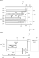
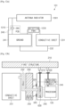
- FIG. 4 is a cross-sectional view illustrating the electronic device 101, according to an embodiment.
- the electronic device 101 may include at least one of the first structure 210 and the second structure 250 of the supporting members 210 and 250, the glass 220, the display panel 230, the conductive sheet 231, the FPCB 232, the PCB 240, a wireless communication circuitry 245, the cover 270, or a feeder 280.
- At least one of components of the electronic device 101 illustrated in FIG. 4 may be the same as or similar to at least one of components of the electronic device 101 of FIG. 3 , and the duplicated description thereof may not be repeated below.
- the FPCB 232 may pass through the second structure 250.
- the FPCB 232 may extend from the conductive sheet 231 in the direction of the first surface S1 of the second structure 250.
- At least one via hole 251 may be formed in at least a portion of the second structure 250 to allow the FPCB 232 to pass therethrough.
- the FPCB 232 may extend at least partially to the second surface of the second structure 250 through the via hole 251 formed in the second structure 250.
- the display panel 230 may be interposed between the glass 220 and the conductive sheet 231.
- the display panel 230 may be spaced apart from the first structure 210 of the supporting members 210 and 250 by a first distance D1 in the first direction (e.g., a Y axis direction).
- a first distance D1 in the first direction (e.g., a Y axis direction).
- the conductive sheet 231 is connected with the ground 241 using the first connection part 310, even if the display panel 230 extends in the direction of the first structure 210, the display panel 230 may be prevented from and/or reduce being pressed by the first connection part 310.
- the first distance D1 is decreased, a screen having the reduced bezel of the electronic device may be provided for a user.
- the second structure 250 may be spaced apart from the first structure 210 in the first direction by a second distance D2.
- the second distance D2 may be greater than the first distance D1.
- the PCB 240 may be interposed between the second structure 250 and the cover 270.
- the first connection part 310 and the second connection part 320 may be disposed on the PCB 240 in the direction of a Z axis.
- the second structure 250 may be interposed between the conductive sheet 231 and the PCB 240.
- the second structure 250 may have at least one via hole 251.
- the FPCB 232 may extend in the direction of the Z axis from the first surface S1 of the second structure 250 to the second surface S2 of the second structure 250 through the via hole 251.
- An adhesive layer 233 may be interposed between the second structure 250 and the conductive sheet 231 in such a manner that the adhesive layer 233 is prevented from or avoids overlapping the via hole 251.
- the adhesive layer 233 may couple the second structure 250 to the conductive sheet 231.
- the first connection part 310 may connect the FPCB 232 with the ground 241 of the PCB 240.
- the first connection part 310 may protrude, for example, from the PCB 240. At least a portion of the first connection part 310 may make contact with at least a portion of the FPCB 232. For example, a top surface of the first connection part 310 may make contact with a part of the FPCB 232 extending through the via hole 251.
- the FPCB 232 may include one or more conductive contacts to be electrically connected with the first connection part 310.
- the conductive contacts may make contact with the upper portion of the first connection part 310.
- the second connection part 320 may electrically connect the ground 241 with the second structure 250.
- the second connection part 320 may protrude, for example, from the PCB 240. At least a portion of the second connection part 320 may make contact with the second surface S2 of the second structure 250.
- the third connection part 330 may connect the feeder 280 with the first structure 210.
- the third connection part 330 may be a power feeding line to feed power to the first structure 210.
- the third connection part 330 may be implemented with a C-clip, a structure extending from the first structure 210, a pogo pin, or a screw.
- the third connection part 330 may be connected with the first structure 210 at a contact 331.
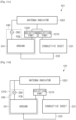
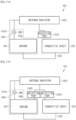
- FIG. 5 is a diagram illustrating the first structure 210, the PCB 240, and the conductive sheet 231 of the electronic device 101, according to an embodiment. At least one of components of the electronic device 101 illustrated in FIG. 5 may be the same as or similar to at least one of components of the electronic device 101 of FIGS. 3 and 4 , and the duplicated description thereof may not be repeated below.
- the first structure 210 may form the edge of the side surface of the electronic device 101.
- the first structure 210 may include the metal portion 211 and insulation portions 212 and 213.
- the metal portion 211 may be fed with power from the feeder 280 using the third connection part 330 and may radiate the signal having the specific frequency.
- the metal portion 211 may be connected with the ground 241 of the PCB 240.
- the insulation portions 212 and 213 may be disposed at opposite sides of the metal portion 211 to electrically isolate the metal portion 211 from other components of the electronic device 101.
- the PCB 240 may include the feeder 280, the ground 241, and a switch 510.
- the feeder 280 may transmit and/or receive a signal having a specific frequency.
- the feeder 280 may apply the signal having the specific frequency to the metal portion 211.
- the ground 241 is connected with the metal portion 211 to function as the ground of the antenna.
- the switch 510 may selectively connect the metal portion 211 with the ground 241 or may selectively connect the metal portion 211 with the conductive sheet 231.
- the third connection part 330 may connect the feeder 280 with the metal portion 211.
- the third connection part 330 may form at least a portion of an electrical path allowing the feeder 280 to apply the signal having the specific frequency to the metal portion 211.
- the conductive sheet 231 may be electrically connected with the ground 241 of the PCB 240 using the first connection part 310.
- the conductive sheet 231 may be directly connected with the metal portion 211 using the switch 510.
- the conductive sheet 231 may be connected with the ground 241 or the metal portion 211 to function as a portion of the antenna.
- the radiation efficiency of the antenna toward the front side of the electronic device 101 may be improved.
- FIG. 6 is a diagram illustrating the display panel 230, the conductive sheet 231, and the FPCB 232 of the electronic device 101, according to an embodiment.
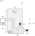
- FIG. 7 is a diagram illustrating the second structure 250, the FPCB 232, the PCB 240, a first metal bezel 710, and a second metal bezel 720 of the electronic device 101, according to an embodiment.
- the conductive sheet 231 may be disposed on the display panel 230.
- the FPCB 232 may extend from one side of the display panel 230.
- the FPCB 232 may be electrically connected with the conductive sheet 231.
- the FPCB 232 may include ground contacts 610 and 620 electrically connected with the ground 241 of at least PCB 240.
- the FPCB 232 may include the first ground contact 610 connected with the ground 241 and the second ground contact 620 connected with the ground 241 at an area closer to an edge of the ground 241 than the first ground contact 610.
- the first ground contact 610 and the second ground contact 620 may include, for example, metal terminals.
- the FPCB 232 may include a connector 630.
- the connector 630 may receive image data from at least one processor (e.g., the processor 120 of FIG. 1 ) to operate the display panel 230 and may supply the data to the display panel 230.
- the connector 630 may electrically connect the ground 241 of the PCB 240 with the conductive sheet 231.
- the connector 630 may be disposed on the FPCB 232. Accordingly, the connector 630 may be electrically connected with the ground 241.
- the second structure 250 may include at least one of via holes 251 and 252.
- the via holes 251 and 252 may pass through from the first surface of the second structure 250 to the second surface of the second structure 250.
- the FPCB 232 may extend from the first surface of the second structure 250 to the second surface of the second structure 250 through the via holes 251 and 252
- first ground contact 610 and the second ground contact 620 may be formed on at least a portion of the FPCB 232.
- the first ground contact 610 and the second ground contact 620 may be arranged to be adjacent to the PCB 240.
- the first ground contact 610 and the second ground contact 620 may be connected with the ground 241.
- the second structure 250 may be electrically connected with the ground 241.
- first metal bezel 710 and the second metal bezel 720 may be included in the metal portion 211 of the first structure 210.
- the first metal bezel 710 and the second metal bezel 720 may function as radiators of the antenna.
- the first metal bezel 710 may be connected with the feeder 280.
- the feeder 280 may be disposed in the PCB 240.
- the first metal bezel 710 may receive power from the feeder 280 to radiate a signal having a specific frequency band.
- the first metal bezel 710 may be connected with the first ground contact 610.
- the first metal bezel 710 may be connected with the FPCB 232 through the first ground contact 610.
- the second metal bezel 720 may be connected with the feeder 280.
- the second metal bezel 720 may receive power from the feeder 280 to radiate a signal having a specific frequency band.
- the second metal bezel 720 may be connected with the second ground contact 620.
- the second metal bezel 720 may be connected with the FPCB 232 through the second ground contact 620
- the FPCB 232 is connected with the conductive sheet 231 such that the conductive sheet 231 functions as the ground and/or the radiator or contributes to the functions of the ground and/or the radiator.
- FIG. 8 is an exploded perspective view illustrating an example electronic device 800, according to another embodiment.
- FIG. 9 is a cross sectional view of the electronic device 800, according to another embodiment.
- the electronic device 800 may include a glass 820, a display panel 830, a conductive sheet 831, an FPCB 832, a PCB 840, a housing 850, a short-range communication circuit 860, a supporting member 870, a wireless communication circuitry 245, a first connection part 910, a second connection part 920, and a third connection part 930.
- At least one of components of the electronic device 800 illustrated in FIG. 9 may be the same as or similar to at least one of components of the electronic device 101 of FIGS. 3 and 4 , and the duplicated description thereof will not be repeated here.
- the housing 850 may include a side member 851 and a rear plate 852.
- the side member 851 may form a side surface of the electronic device 800.
- the rear plate 852 may form a rear surface of the electronic device 800.
- the side member 851 and the rear plate 852 may be integrally formed. Accordingly, the housing 850 may be formed in a single structure.
- the supporting member 870 may be disposed inside the electronic device 800.
- the supporting member 870 may form the mounting structure for parts of the electronic device 800.
- the supporting member 870 may separate the glass 820, the display panel 830, the conductive sheet 831, and the FPCB 832 from the PCB 840 in terms of position.
- the glass 820, the display panel 830, the conductive sheet 831, and the FPCB 832 may be disposed on one surface of the supporting member 870 and the PCB 840 may be disposed on an opposite surface of the PCB 840.
- the supporting member 870 may include at least one via hole 871 or a recess to allow a connection member, which electrically connects parts disposed on opposite surfaces with each other, to pass therethrough.
- the supporting member 870 may include the via hole 871 bored from the first surface S1 to the second surface S2.
- the FPCB may include a connector that connects the at least one processor with the PCB such that the at least one processor operates the display panel, and the connector may electrically connect the ground of the PCB with the conductive sheet.
- the FPCB may have a second path extending from the first surface to the second surface through the at least one via hole or recess of the supporting member, and the second path of the FPCB extending to the second surface may be electrically connected with the metal portion of the side portion directly or through a switch.
- the FPCB may protrude on a second surface of the supporting member and ground contacts may be formed on at least a portion of a protruding surface of the FPCB.
- the ground contacts may be connected with the ground of the PCB.
- the FPCB may include a connector that connects the at least one processor with the PCB such that the at least one processor operates the display panel, and the connector may electrically connect the ground of the PCB with the conductive sheet.
- the electrical path may feed a first current from the wireless communication circuitry to the antenna radiator, or feed a second current corresponding to the first current from the antennal radiator to the conductive sheet.
- the electrical path electrically may connect the conductive sheet with the ground of the PCB such that the conductive sheet is configured to be a ground of the electrical path.
- the electrical path may include a feeding path extending from the wireless communication circuitry toward the antenna radiator, and a ground path extending from the metal frame toward the conductive sheet.
- the antenna radiator may radiate the signal having the specific frequency band.
- the electronic device may be one of various types of electronic devices.
- the electronic devices may include, for example, a portable communication device (e.g., a smartphone), a computer device, a portable multimedia device, a portable medical device, a camera, a wearable device, or a home appliance. According to an embodiment of the disclosure, the electronic devices are not limited to those described above.
- each of such phrases as “A or B,” “at least one of A and B,” “at least one of A or B,” “A, B, or C,” “at least one of A, B, and C,” and “at least one of A, B, or C,” may include any one of, or all possible combinations of the items enumerated together in a corresponding one of the phrases.
- such terms as “1st” and “2nd,” or “first” and “second” may be used to simply distinguish a corresponding component from another, and does not limit the components in other aspect (e.g., importance or order).
- an element e.g., a first element
- the element may be coupled with the other element directly (e.g., wiredly), wirelessly, or via a third element.
- module may include a unit implemented in hardware, software, or firmware, and may interchangeably be used with other terms, for example, “logic,” “logic block,” “part,” or “circuitry”.
- a module may be a single integral component, or a minimum unit or part thereof, adapted to perform one or more functions.
- the module may be implemented in a form of an application-specific integrated circuit (ASIC).
- ASIC application-specific integrated circuit
- Various embodiments as set forth herein may be implemented as software (e.g., the program 140) including one or more instructions that are stored in a storage medium (e.g., internal memory 136 or external memory 138) that is readable by a machine (e.g., the electronic device 101).
- a processor(e.g., the processor 120) of the machine e.g., the electronic device 101
- the one or more instructions may include a code generated by a compiler or a code executable by an interpreter.
- the machine-readable storage medium may be provided in the form of a non-transitory storage medium.
- the "non-transitory” storage medium is a tangible device, and does not include a signal (e.g., an electromagnetic wave), but this term does not differentiate between where data is semi-permanently stored in the storage medium and where the data is temporarily stored in the storage medium.
- a method may be included and provided in a computer program product.
- the computer program product may be traded as a product between a seller and a buyer.
- the computer program product may be distributed in the form of a machine-readable storage medium (e.g., compact disc read only memory (CD-ROM)), or be distributed (e.g., downloaded or uploaded) online via an application store (e.g., PlayStore ), or between two user devices (e.g., smart phones) directly. If distributed online, at least part of the computer program product may be temporarily generated or at least temporarily stored in the machine-readable storage medium, such as memory of the manufacturer's server, a server of the application store, or a relay server.
- CD-ROM compact disc read only memory
- an application store e.g., PlayStore
- two user devices e.g., smart phones
- each component e.g., a module or a program of the above-described components may include a single entity or multiple entities. According to various embodiments, one or more of the above-described components may be omitted, or one or more other components may be added. Alternatively or additionally, a plurality of components (e.g., modules or programs) may be integrated into a single component. In such a case, according to various embodiments, the integrated component may still perform one or more functions of each of the plurality of components in the same or similar manner as they are performed by a corresponding one of the plurality of components before the integration.
Landscapes
- Engineering & Computer Science (AREA)
- Microelectronics & Electronic Packaging (AREA)
- Computer Networks & Wireless Communication (AREA)
- Signal Processing (AREA)
- Telephone Set Structure (AREA)
- Devices For Indicating Variable Information By Combining Individual Elements (AREA)
Claims (17)
- Dispositif électronique (101) comprenant :un boîtier comprenant une surface avant du dispositif électronique, la surface avant du dispositif électronique comprenant ou formée d'une plaque de verre (220) ;un écran d'affichage (230) disposé sous la plaque de verre (220) ;une feuille conductrice (231) fixée à l'écran d'affichage (230) ou intégrée à l'écran d'affichage (230) ;un support incluant une première portion (210) comprenant une surface latérale du dispositif électronique et une deuxième portion (250) comprenant un espace de montage pour des parties, où la première portion (210) du support inclut une portion métallique (211) configurée comme une antenne et où la deuxième portion (250) du support inclut une première surface (S1), une deuxième surface (S2) et au moins un trou d'interconnexion (251) ou renfoncement s'étendant de la première surface (S1) à la deuxième surface (S2)une carte de circuit imprimé, PCB (240), incluant une masse (241) ;un circuit de communication sans fil (245) disposé sur le PCB ;au moins un processeur (120) disposé sur le PCB connecté de manière opérationnelle au circuit de communication sans fil ;un PCB flexible, FPCB (232), connecté électriquement à la feuille conductrice et configuré pour connecter de manière opérationnelle l'écran d'affichage avec l'au moins un processeur, etune couverture (270) comprenant une surface arrière du dispositif électronique,où la plaque de verre (220), l'écran d'affichage (230) et la feuille conductrice (231) sont placés sur la première surface (S1) de la deuxième portion (250) du support,où le PCB (240) et la couverture (270) du dispositif électronique sont placés sur la deuxième surface (S2) de la deuxième portion (250),où la deuxième portion (250) du support connecte électriquement le support à la masse (241) du PCB (240) en faisant contact avec l'un des contacts conducteurs du PCB (240) sur au moins un point,où le FPCB (232) inclut un premier chemin s'étendant de la première surface (S1) à la deuxième surface (S2) à travers l'au moins un trou d'interconnexion (251) ou renfoncement de la deuxième portion (250) du support,où le premier chemin du FPCB (232) s'étendant jusqu'à la deuxième surface (S2) connecte électriquement la feuille conductrice (231) à la masse (241) du PCB (240),où la feuille conductrice (231) est connectée électriquement à la portion métallique (211) du support à travers une partie de sélection comprenant un circuit de connexion sélectif, etoù le circuit de communication sans fil (245) est configuré pour recevoir un signal ayant une bande de fréquence spécifique sur la base d'un chemin électrique incluant le circuit de communication sans fil (245), la portion métallique (211) du support, la partie de sélection et la feuille conductrice (231).
- Dispositif électronique selon la revendication 1, où le circuit de communication sans fil (245) est configuré pour alimenter en énergie la portion métallique (211) du support en utilisant un alimentateur (280) disposé dans le PCB (240) et une troisième partie de connexion (330) comprenant un conducteur connecté à l'alimentateur (280).
- Dispositif électronique selon la revendication 1, où le FPCB (232) s'étend d'un côté de l'écran d'affichage (230) et est connecté à l'au moins un processeur (120).
- Dispositif électronique selon la revendication 1, où le FPCB (232) inclut un deuxième chemin s'étendant de la première surface (S1) à la deuxième surface (S2) à travers l'au moins un trou d'interconnexion (251) ou renfoncement de la deuxième portion (250) du support, et
où le deuxième chemin du FPCB (232) s'étendant jusqu'à la deuxième surface (S2) est connecté électriquement à la portion métallique (211) du support directement ou à travers un commutateur (510). - Dispositif électronique selon la revendication 1, où le FPCB (232) fait saillie sur la deuxième surface (S2) de la deuxième portion (250) du support et un contact de masse (610, 620) est pourvu sur au moins une portion d'une surface saillante du FPCB (232), et
où le contact de masse (610, 620) est connecté à la masse (241) du PCB (240). - Dispositif électronique selon la revendication 1, où une première partie de connexion (310) comprenant un conducteur connecté à la masse (241) est pourvue sur une surface du PCB (240) faisant face à la deuxième surface (S2) de la deuxième portion (250) du support, et
où le FPCB (232) est en contact avec la première partie de connexion (310). - Dispositif électronique selon la revendication 1, où le PCB (240) inclut :un alimentateur (280) connecté électriquement au circuit de communication sans fil (245) et configuré pour alimenter en énergie la portion métallique (211) du support,où la masse (241) est espacée de l'alimentateur (280), etoù la masse (241) est connectée à la deuxième portion (250) du support en utilisant une deuxième partie de connexion (320).
- Dispositif électronique selon la revendication 1, où le FPCB (232) inclut un connecteur (630) connectant l'au moins un processeur (120) au PCB (240) de sorte que l'au moins un processeur (120) actionne l'écran d'affichage (230), et
où le connecteur (630) connecte électriquement la masse (241 ) du PCB (240) avec la feuille conductrice (231). - Dispositif électronique selon la revendication 1, où la première portion (210) du support inclut en outre une portion d'isolation (212, 213) disposée dans au moins une extrémité de la portion métallique (211).
- Dispositif électronique (800) comprenant :la surface avant du dispositif électronique (800) comprenant ou formée d'une plaque de verre (820) ;un écran d'affichage (830) disposé sous la plaque de verre (820) ;une feuille conductrice (831) fixée à l'écran d'affichage (830) ou intégrée à l'écran d'affichage (830) ;un boîtier (850) incluant une portion latérale (851) comprenant une surface latérale du dispositif électronique et une plaque arrière (852) comprenant une surface arrière du dispositif électronique, où la portion latérale (851) inclut une portion métallique (211) configurée comme une antenne ;une carte de circuit imprimé, PCB (840), incluant une masse (841) ;un support (870) séparant le verre (820), l'écran d'affichage (830) et la feuille conductrice (831) du PCB (840), où le support (870) inclut une première surface (S1), une deuxième surface (S2) et au moins un trou d'interconnexion (871) ou renfoncement s'étendant de la première surface (S1) à la deuxième surface (S2),un circuit de communication sans fil (245) disposé sur le PCB (840) ;au moins un processeur (120) disposé sur le PCB (840) connecté de manière opérationnelle au circuit de communication sans fil (245) ; etune carte de circuit imprimé flexible, FPCB (832), connectée électriquement à la feuille conductrice (831) et configurée pour connecter de manière opérationnelle l'écran d'affichage (830) à l'au moins un processeur (120),où la plaque de verre (820), l'écran d'affichage (830) et la feuille conductrice (831) sont placés sur la première surface (S1) du support (870),où le PCB (840) est disposé sur la deuxième surface (S2) du support (870),où la plaque arrière (852) connecte électriquement le boîtier (850) à la masse (841) du PCB (840) en faisant contact avec l'un des contacts conducteurs du PCB (840) sur au moins un point,où le FPCB (832) inclut un premier chemin s'étendant de la première surface (S1) du support (870) à la deuxième surface (S2) du support (870) à travers l'au moins un trou d'interconnexion (871) ou renfoncement du support (870),où le premier chemin du FPCB (832) s'étendant jusqu'à la deuxième surface (S2) du support (870) connecte électriquement la feuille conductrice (831) à la masse (841) du PCB (840),où la feuille conductrice (831) est connectée électriquement à la portion métallique (211) de la portion latérale (851) à travers une partie de sélection comprenant un circuit de connexion sélectif, etoù le circuit de communication sans fil (245) est configuré pour recevoir un signal ayant une bande de fréquence spécifique sur la base d'un chemin électrique comprenant le circuit de communication sans fil (245), la portion métallique (211) de la portion latérale (851), la partie de sélection et la feuille conductrice (831).
- Dispositif électronique selon la revendication 10, où le circuit de communication sans fil (245) est configuré pour alimenter en énergie la portion métallique (211) de la portion latérale (851) en utilisant un alimentateur (280) disposé dans le PCB (840) et une troisième partie de connexion (330) comprenant un conducteur connecté à l'alimentateur (280).
- Dispositif électronique selon la revendication 10, où le FPCB (832) s'étend d'un côté de l'écran d'affichage (830) et est connecté à l'au moins un processeur (120).
- Dispositif électronique selon la revendication 10, où le FPCB (832) inclut un deuxième chemin s'étendant de la première surface (S1) à la deuxième surface (S2) à travers l'au moins un trou d'interconnexion (871) ou renfoncement du support (870), et
où le deuxième chemin du FPCB (832) s'étendant jusqu'à la deuxième surface est connecté électriquement à la portion métallique (211) de la portion latérale (511) directement ou à travers un commutateur. - Dispositif électronique selon la revendication 11, où le FPCB (832) fait saillie sur une deuxième surface (S2) du support (870) et un contact de masse est pourvu sur au moins une portion d'une surface saillante du FPCB (832), et
où le contact de masse est connecté à la masse du PCB (840). - Dispositif électronique selon la revendication 11, où une première partie de connexion comprenant un conducteur connecté à la masse (841) est pourvue sur une surface du PCB (840) faisant face à la deuxième surface du support, et
où le FPCB (832) est en contact avec la première partie de connexion. - Dispositif électronique selon la revendication 11, où le FPCB (832) inclut un connecteur connectant l'au moins un processeur au PCB (840) de sorte que l'au moins un processeur actionne l'écran d'affichage, et
où le connecteur connecte électriquement la masse du PCB (840) à la feuille conductrice (831). - Dispositif électronique selon la revendication 10, où la portion latérale (851) inclut en outre une portion d'isolation (212, 213) séparant la portion métallique (211) d'une portion restante du boîtier (850).
Applications Claiming Priority (2)
| Application Number | Priority Date | Filing Date | Title |
|---|---|---|---|
| KR1020180127098A KR102613054B1 (ko) | 2018-10-24 | 2018-10-24 | 디스플레이 패널의 도전 시트와 연결된 안테나를 포함하는 전자 장치 |
| PCT/KR2019/013550 WO2020085710A1 (fr) | 2018-10-24 | 2019-10-16 | Dispositif électronique comprenant une antenne connectée à une feuille conductrice d'un écran d'affichage |
Publications (3)
| Publication Number | Publication Date |
|---|---|
| EP3834403A1 EP3834403A1 (fr) | 2021-06-16 |
| EP3834403A4 EP3834403A4 (fr) | 2021-10-13 |
| EP3834403B1 true EP3834403B1 (fr) | 2024-11-27 |
Family
ID=70326500
Family Applications (1)
| Application Number | Title | Priority Date | Filing Date |
|---|---|---|---|
| EP19876180.1A Active EP3834403B1 (fr) | 2018-10-24 | 2019-10-16 | Dispositif électronique comprenant une antenne connectée à une feuille conductrice d'un écran d'affichage |
Country Status (5)
| Country | Link |
|---|---|
| US (1) | US10971809B2 (fr) |
| EP (1) | EP3834403B1 (fr) |
| KR (1) | KR102613054B1 (fr) |
| CN (1) | CN112913216B (fr) |
| WO (1) | WO2020085710A1 (fr) |
Families Citing this family (29)
| Publication number | Priority date | Publication date | Assignee | Title |
|---|---|---|---|---|
| USD922372S1 (en) * | 2018-07-27 | 2021-06-15 | Samsung Electronics Co., Ltd. | Electronic device |
| USD922373S1 (en) * | 2018-07-27 | 2021-06-15 | Samsung Electronics Co., Ltd. | Electronic device |
| KR102759982B1 (ko) * | 2020-05-06 | 2025-02-03 | 삼성전자주식회사 | 안테나를 포함하는 전자 장치 |
| US11592870B2 (en) * | 2020-06-11 | 2023-02-28 | Apple Inc. | Electronic device architecture and components |
| US12174660B2 (en) | 2020-06-11 | 2024-12-24 | Apple Inc. | Electronic device |
| CN113948863B (zh) * | 2020-07-16 | 2025-12-30 | 深圳富泰宏精密工业有限公司 | 信号馈入组件,天线模块及电子设备 |
| KR102825633B1 (ko) | 2020-07-31 | 2025-06-26 | 삼성전자주식회사 | 안테나 및 그것을 포함하는 전자 장치 |
| KR102750634B1 (ko) | 2020-08-03 | 2025-01-08 | 삼성전자 주식회사 | 안테나 및 분절부를 포함하는 전자 장치 |
| KR102837741B1 (ko) * | 2020-08-04 | 2025-07-23 | 삼성전자주식회사 | 연성 기판을 포함하는 전자 장치 |
| KR102864057B1 (ko) * | 2020-08-04 | 2025-09-24 | 삼성전자주식회사 | 전자 장치에 있어서 안테나 스위칭 방법 및 그 장치 |
| KR102792604B1 (ko) | 2020-08-04 | 2025-04-08 | 삼성전자주식회사 | 도전성 하우징 및 안테나를 포함하는 전자 장치 |
| KR102911357B1 (ko) * | 2020-11-02 | 2026-01-12 | 삼성전자주식회사 | 안테나를 포함하는 웨어러블 전자 장치 |
| KR102752738B1 (ko) | 2020-11-11 | 2025-01-10 | 삼성전자주식회사 | 하우징을 포함하는 전자 장치 |
| KR102893858B1 (ko) | 2020-12-02 | 2025-12-03 | 삼성전자 주식회사 | 유연 인쇄 회로 기판을 포함하는 안테나 급전 구조 및 그를 포함하는 전자장치 |
| EP4224280A4 (fr) * | 2020-12-04 | 2024-04-10 | Samsung Electronics Co., Ltd. | Dispositif électronique comprenant un écran souple |
| KR102885608B1 (ko) * | 2021-03-23 | 2025-11-13 | 삼성전자 주식회사 | 도전성 소재로 형성된 프레임과 인접하게 배치되는 기판 부재를 포함하는 전자 장치 |
| EP4250881B1 (fr) | 2021-03-23 | 2025-09-24 | Samsung Electronics Co., Ltd. | Dispositif électronique comprenant un élément de substrat agencé pour être adjacent à un cadre formé à partir d'un matériau conducteur |
| WO2022203453A1 (fr) * | 2021-03-25 | 2022-09-29 | 삼성전자 주식회사 | Dispositif électronique comprenant une antenne |
| CN117044037A (zh) | 2021-03-25 | 2023-11-10 | 三星电子株式会社 | 包括天线的电子装置 |
| KR102899707B1 (ko) * | 2021-05-10 | 2025-12-15 | 삼성디스플레이 주식회사 | 표시 장치 |
| US12328811B2 (en) | 2021-07-27 | 2025-06-10 | Samsung Electronics Co., Ltd | Insulating member arrangement structure and electronic device including the same |
| KR102860389B1 (ko) * | 2021-08-10 | 2025-09-16 | 삼성전자주식회사 | 동축 케이블을 포함하는 전자 장치 |
| EP4451465A4 (fr) * | 2022-01-17 | 2025-04-16 | Samsung Electronics Co., Ltd | Dispositif électronique comprenant une antenne |
| WO2023195739A1 (fr) * | 2022-04-04 | 2023-10-12 | 삼성전자 주식회사 | Structure d'affichage et dispositif électronique comprenant une structure d'affichage |
| US12556627B2 (en) * | 2022-07-12 | 2026-02-17 | Samsung Electronics Co., Ltd. | Electronic device including housing having dissimilar metals |
| TWI799339B (zh) * | 2022-08-22 | 2023-04-11 | 華碩電腦股份有限公司 | 手持式電子裝置 |
| CN121128157A (zh) * | 2023-05-04 | 2025-12-12 | 三星电子株式会社 | 天线和包括天线的电子装置 |
| WO2025063560A1 (fr) * | 2023-09-21 | 2025-03-27 | 삼성전자주식회사 | Dispositif électronique comprenant une antenne |
| WO2025220905A1 (fr) * | 2024-04-19 | 2025-10-23 | 삼성전자 주식회사 | Dispositif électronique à porter sur soi comprenant une antenne |
Family Cites Families (26)
| Publication number | Priority date | Publication date | Assignee | Title |
|---|---|---|---|---|
| JP4552565B2 (ja) | 2004-09-03 | 2010-09-29 | 日本電気株式会社 | フレキシブル配線基板及び折り畳み式電子機器 |
| KR20090004235A (ko) * | 2007-07-06 | 2009-01-12 | 엘지전자 주식회사 | 휴대 단말기 |
| CN101667373B (zh) * | 2009-09-28 | 2011-07-27 | 友达光电(厦门)有限公司 | 显示装置 |
| JP2012079729A (ja) * | 2010-09-30 | 2012-04-19 | Fujitsu Ltd | 電子装置 |
| CN102496773B (zh) * | 2011-10-31 | 2014-02-12 | 青岛海信移动通信技术股份有限公司 | 一种提高移动通信天线效率的方法及移动通信终端 |
| JP2013239812A (ja) * | 2012-05-14 | 2013-11-28 | Sharp Corp | 携帯端末 |
| KR101467196B1 (ko) * | 2013-03-29 | 2014-12-01 | 주식회사 팬택 | 전도성 테두리를 이용한 다중 대역 안테나를 포함하는 단말기 |
| KR102119660B1 (ko) * | 2013-10-17 | 2020-06-08 | 엘지전자 주식회사 | 이동 단말기 |
| KR20160024631A (ko) * | 2014-08-26 | 2016-03-07 | 삼성전자주식회사 | 다중대역 루프 안테나 및 이를 구비한 전자 장치 |
| KR102314790B1 (ko) * | 2015-02-26 | 2021-10-20 | 삼성전자주식회사 | 안테나 장치를 포함하는 전자 장치 |
| KR102415651B1 (ko) * | 2015-07-01 | 2022-07-01 | 엘지전자 주식회사 | 이동 단말기 |
| KR102514770B1 (ko) * | 2015-10-02 | 2023-03-29 | 삼성전자주식회사 | 방수 구조를 포함하는 전자 장치 |
| KR102164704B1 (ko) * | 2015-11-13 | 2020-10-12 | 삼성전자주식회사 | 금속 프레임 안테나를 구비한 전자 장치 |
| KR102507472B1 (ko) | 2016-02-26 | 2023-03-09 | 삼성전자주식회사 | 디스플레이를 구비한 전자 장치의 안테나 |
| KR102503223B1 (ko) * | 2016-03-10 | 2023-02-24 | 삼성전자주식회사 | 연결 부재 및 이를 포함하는 전자 장치 |
| KR102466002B1 (ko) * | 2016-04-19 | 2022-11-11 | 삼성전자주식회사 | 안테나를 포함하는 전자 장치 |
| KR102503231B1 (ko) * | 2016-07-14 | 2023-02-27 | 삼성전자주식회사 | 전자 장치의 입력 모듈 배선 구조 |
| US10044097B2 (en) * | 2016-07-21 | 2018-08-07 | Chiun Mai Communication Systems, Inc. | Antenna structure and wireless communication device using same |
| KR102332117B1 (ko) * | 2016-07-21 | 2021-11-30 | 삼성전자주식회사 | 무선 통신을 위한 안테나 및 이를 포함하는 전자 장치 |
| KR102532660B1 (ko) * | 2016-09-19 | 2023-05-16 | 삼성전자주식회사 | 안테나를 포함하는 전자 장치 |
| KR101841583B1 (ko) * | 2016-12-05 | 2018-03-26 | 삼성전자주식회사 | 전자 장치의 모듈 배치 구조 |
| CN108270069B (zh) * | 2016-12-30 | 2020-06-02 | 北京小米移动软件有限公司 | 天线模组和电子设备 |
| CN107728365A (zh) * | 2017-10-31 | 2018-02-23 | 武汉华星光电技术有限公司 | 窄边框显示面板及显示装置 |
| CN207427565U (zh) * | 2017-11-10 | 2018-05-29 | 广东欧珀移动通信有限公司 | 一种柔性电路板接地组件及移动终端 |
| CN107979665A (zh) * | 2017-11-29 | 2018-05-01 | 北京小米移动软件有限公司 | 移动终端 |
| CN108540616B (zh) * | 2018-06-22 | 2020-05-12 | Oppo广东移动通信有限公司 | 显示屏组件及电子设备 |
-
2018
- 2018-10-24 KR KR1020180127098A patent/KR102613054B1/ko active Active
-
2019
- 2019-10-16 EP EP19876180.1A patent/EP3834403B1/fr active Active
- 2019-10-16 WO PCT/KR2019/013550 patent/WO2020085710A1/fr not_active Ceased
- 2019-10-16 CN CN201980069996.2A patent/CN112913216B/zh active Active
- 2019-10-23 US US16/661,071 patent/US10971809B2/en active Active
Also Published As
| Publication number | Publication date |
|---|---|
| EP3834403A1 (fr) | 2021-06-16 |
| KR102613054B1 (ko) | 2023-12-15 |
| KR20200046246A (ko) | 2020-05-07 |
| CN112913216B (zh) | 2023-04-11 |
| WO2020085710A1 (fr) | 2020-04-30 |
| EP3834403A4 (fr) | 2021-10-13 |
| US10971809B2 (en) | 2021-04-06 |
| US20200136243A1 (en) | 2020-04-30 |
| CN112913216A (zh) | 2021-06-04 |
Similar Documents
| Publication | Publication Date | Title |
|---|---|---|
| EP3834403B1 (fr) | Dispositif électronique comprenant une antenne connectée à une feuille conductrice d'un écran d'affichage | |
| US12237568B2 (en) | Electronic device including 5G antenna module | |
| US11855674B2 (en) | Electronic device comprising antenna for wireless communication | |
| US12470648B2 (en) | Plurality of antennas and electronic device comprising same | |
| US11367945B2 (en) | Electronic device and method comprising antenna | |
| EP3716587B1 (fr) | Dispositif électronique comprenant une antenne et procédé d'émission ou de réception de signal | |
| US12057619B2 (en) | Electronic device having side key comprising antenna | |
| US10833403B2 (en) | Antenna and electronic device including same | |
| EP3794808B1 (fr) | Dispositif électronique comprenant une carte de circuit imprimé souple adjacente à une antenne | |
| US11056769B2 (en) | Electronic device comprising antenna | |
| EP3820126A1 (fr) | Dispositif électronique comprenant un module d'antenne 5g | |
| US11824260B2 (en) | Electronic device comprising antenna | |
| US12015727B2 (en) | Electronic device including reinforcement member | |
| US12225149B2 (en) | Electronic device comprising antenna | |
| US11916290B2 (en) | Structure for reducing interference between antennas and electronic device comprising the same | |
| KR102758022B1 (ko) | 안테나 및 이를 구비한 전자 장치 |
Legal Events
| Date | Code | Title | Description |
|---|---|---|---|
| STAA | Information on the status of an ep patent application or granted ep patent |
Free format text: STATUS: THE INTERNATIONAL PUBLICATION HAS BEEN MADE |
|
| PUAI | Public reference made under article 153(3) epc to a published international application that has entered the european phase |
Free format text: ORIGINAL CODE: 0009012 |
|
| STAA | Information on the status of an ep patent application or granted ep patent |
Free format text: STATUS: REQUEST FOR EXAMINATION WAS MADE |
|
| 17P | Request for examination filed |
Effective date: 20210309 |
|
| AK | Designated contracting states |
Kind code of ref document: A1 Designated state(s): AL AT BE BG CH CY CZ DE DK EE ES FI FR GB GR HR HU IE IS IT LI LT LU LV MC MK MT NL NO PL PT RO RS SE SI SK SM TR |
|
| A4 | Supplementary search report drawn up and despatched |
Effective date: 20210913 |
|
| RIC1 | Information provided on ipc code assigned before grant |
Ipc: H05K 1/02 20060101ALI20210907BHEP Ipc: H05K 1/18 20060101ALI20210907BHEP Ipc: H05K 1/14 20060101ALI20210907BHEP Ipc: H01Q 1/48 20060101ALI20210907BHEP Ipc: H01Q 1/38 20060101ALI20210907BHEP Ipc: H01Q 1/52 20060101ALI20210907BHEP Ipc: H01Q 1/24 20060101ALI20210907BHEP Ipc: H04M 1/02 20060101AFI20210907BHEP |
|
| DAV | Request for validation of the european patent (deleted) | ||
| DAX | Request for extension of the european patent (deleted) | ||
| REG | Reference to a national code |
Ref country code: DE Ref legal event code: R079 Ipc: H01Q0001240000 Ref country code: DE Ref legal event code: R079 Ref document number: 602019062743 Country of ref document: DE Free format text: PREVIOUS MAIN CLASS: H04M0001020000 Ipc: H01Q0001240000 |
|
| GRAP | Despatch of communication of intention to grant a patent |
Free format text: ORIGINAL CODE: EPIDOSNIGR1 |
|
| STAA | Information on the status of an ep patent application or granted ep patent |
Free format text: STATUS: GRANT OF PATENT IS INTENDED |
|
| RIC1 | Information provided on ipc code assigned before grant |
Ipc: H05K 1/18 20060101ALN20240523BHEP Ipc: H05K 1/02 20060101ALN20240523BHEP Ipc: H01Q 1/52 20060101ALI20240523BHEP Ipc: H05K 1/14 20060101ALI20240523BHEP Ipc: H04M 1/02 20060101ALI20240523BHEP Ipc: H01Q 1/48 20060101ALI20240523BHEP Ipc: H01Q 1/38 20060101ALI20240523BHEP Ipc: H01Q 1/24 20060101AFI20240523BHEP |
|
| RIC1 | Information provided on ipc code assigned before grant |
Ipc: H05K 1/18 20060101ALN20240524BHEP Ipc: H05K 1/02 20060101ALN20240524BHEP Ipc: H01Q 1/52 20060101ALI20240524BHEP Ipc: H05K 1/14 20060101ALI20240524BHEP Ipc: H04M 1/02 20060101ALI20240524BHEP Ipc: H01Q 1/48 20060101ALI20240524BHEP Ipc: H01Q 1/38 20060101ALI20240524BHEP Ipc: H01Q 1/24 20060101AFI20240524BHEP |
|
| RIC1 | Information provided on ipc code assigned before grant |
Ipc: H05K 1/18 20060101ALN20240606BHEP Ipc: H05K 1/02 20060101ALN20240606BHEP Ipc: H01Q 1/52 20060101ALI20240606BHEP Ipc: H05K 1/14 20060101ALI20240606BHEP Ipc: H04M 1/02 20060101ALI20240606BHEP Ipc: H01Q 1/48 20060101ALI20240606BHEP Ipc: H01Q 1/38 20060101ALI20240606BHEP Ipc: H01Q 1/24 20060101AFI20240606BHEP |
|
| INTG | Intention to grant announced |
Effective date: 20240618 |
|
| GRAS | Grant fee paid |
Free format text: ORIGINAL CODE: EPIDOSNIGR3 |
|
| GRAA | (expected) grant |
Free format text: ORIGINAL CODE: 0009210 |
|
| STAA | Information on the status of an ep patent application or granted ep patent |
Free format text: STATUS: THE PATENT HAS BEEN GRANTED |
|
| AK | Designated contracting states |
Kind code of ref document: B1 Designated state(s): AL AT BE BG CH CY CZ DE DK EE ES FI FR GB GR HR HU IE IS IT LI LT LU LV MC MK MT NL NO PL PT RO RS SE SI SK SM TR |
|
| REG | Reference to a national code |
Ref country code: GB Ref legal event code: FG4D |
|
| REG | Reference to a national code |
Ref country code: CH Ref legal event code: EP |
|
| REG | Reference to a national code |
Ref country code: IE Ref legal event code: FG4D |
|
| REG | Reference to a national code |
Ref country code: DE Ref legal event code: R096 Ref document number: 602019062743 Country of ref document: DE |
|
| REG | Reference to a national code |
Ref country code: LT Ref legal event code: MG9D |
|
| REG | Reference to a national code |
Ref country code: NL Ref legal event code: MP Effective date: 20241127 |
|
| PG25 | Lapsed in a contracting state [announced via postgrant information from national office to epo] |
Ref country code: HR Free format text: LAPSE BECAUSE OF FAILURE TO SUBMIT A TRANSLATION OF THE DESCRIPTION OR TO PAY THE FEE WITHIN THE PRESCRIBED TIME-LIMIT Effective date: 20241127 Ref country code: PT Free format text: LAPSE BECAUSE OF FAILURE TO SUBMIT A TRANSLATION OF THE DESCRIPTION OR TO PAY THE FEE WITHIN THE PRESCRIBED TIME-LIMIT Effective date: 20250327 Ref country code: IS Free format text: LAPSE BECAUSE OF FAILURE TO SUBMIT A TRANSLATION OF THE DESCRIPTION OR TO PAY THE FEE WITHIN THE PRESCRIBED TIME-LIMIT Effective date: 20250327 |
|
| PG25 | Lapsed in a contracting state [announced via postgrant information from national office to epo] |
Ref country code: FI Free format text: LAPSE BECAUSE OF FAILURE TO SUBMIT A TRANSLATION OF THE DESCRIPTION OR TO PAY THE FEE WITHIN THE PRESCRIBED TIME-LIMIT Effective date: 20241127 Ref country code: NL Free format text: LAPSE BECAUSE OF FAILURE TO SUBMIT A TRANSLATION OF THE DESCRIPTION OR TO PAY THE FEE WITHIN THE PRESCRIBED TIME-LIMIT Effective date: 20241127 |
|
| REG | Reference to a national code |
Ref country code: AT Ref legal event code: MK05 Ref document number: 1746647 Country of ref document: AT Kind code of ref document: T Effective date: 20241127 |
|
| PG25 | Lapsed in a contracting state [announced via postgrant information from national office to epo] |
Ref country code: BG Free format text: LAPSE BECAUSE OF FAILURE TO SUBMIT A TRANSLATION OF THE DESCRIPTION OR TO PAY THE FEE WITHIN THE PRESCRIBED TIME-LIMIT Effective date: 20241127 |
|
| PG25 | Lapsed in a contracting state [announced via postgrant information from national office to epo] |
Ref country code: ES Free format text: LAPSE BECAUSE OF FAILURE TO SUBMIT A TRANSLATION OF THE DESCRIPTION OR TO PAY THE FEE WITHIN THE PRESCRIBED TIME-LIMIT Effective date: 20241127 |
|
| PG25 | Lapsed in a contracting state [announced via postgrant information from national office to epo] |
Ref country code: NO Free format text: LAPSE BECAUSE OF FAILURE TO SUBMIT A TRANSLATION OF THE DESCRIPTION OR TO PAY THE FEE WITHIN THE PRESCRIBED TIME-LIMIT Effective date: 20250227 |
|
| PG25 | Lapsed in a contracting state [announced via postgrant information from national office to epo] |
Ref country code: GR Free format text: LAPSE BECAUSE OF FAILURE TO SUBMIT A TRANSLATION OF THE DESCRIPTION OR TO PAY THE FEE WITHIN THE PRESCRIBED TIME-LIMIT Effective date: 20250228 Ref country code: LV Free format text: LAPSE BECAUSE OF FAILURE TO SUBMIT A TRANSLATION OF THE DESCRIPTION OR TO PAY THE FEE WITHIN THE PRESCRIBED TIME-LIMIT Effective date: 20241127 Ref country code: AT Free format text: LAPSE BECAUSE OF FAILURE TO SUBMIT A TRANSLATION OF THE DESCRIPTION OR TO PAY THE FEE WITHIN THE PRESCRIBED TIME-LIMIT Effective date: 20241127 |
|
| PG25 | Lapsed in a contracting state [announced via postgrant information from national office to epo] |
Ref country code: PL Free format text: LAPSE BECAUSE OF FAILURE TO SUBMIT A TRANSLATION OF THE DESCRIPTION OR TO PAY THE FEE WITHIN THE PRESCRIBED TIME-LIMIT Effective date: 20241127 |
|
| PG25 | Lapsed in a contracting state [announced via postgrant information from national office to epo] |
Ref country code: RS Free format text: LAPSE BECAUSE OF FAILURE TO SUBMIT A TRANSLATION OF THE DESCRIPTION OR TO PAY THE FEE WITHIN THE PRESCRIBED TIME-LIMIT Effective date: 20250227 |
|
| PG25 | Lapsed in a contracting state [announced via postgrant information from national office to epo] |
Ref country code: SM Free format text: LAPSE BECAUSE OF FAILURE TO SUBMIT A TRANSLATION OF THE DESCRIPTION OR TO PAY THE FEE WITHIN THE PRESCRIBED TIME-LIMIT Effective date: 20241127 |
|
| PG25 | Lapsed in a contracting state [announced via postgrant information from national office to epo] |
Ref country code: DK Free format text: LAPSE BECAUSE OF FAILURE TO SUBMIT A TRANSLATION OF THE DESCRIPTION OR TO PAY THE FEE WITHIN THE PRESCRIBED TIME-LIMIT Effective date: 20241127 |
|
| PG25 | Lapsed in a contracting state [announced via postgrant information from national office to epo] |
Ref country code: EE Free format text: LAPSE BECAUSE OF FAILURE TO SUBMIT A TRANSLATION OF THE DESCRIPTION OR TO PAY THE FEE WITHIN THE PRESCRIBED TIME-LIMIT Effective date: 20241127 |
|
| PG25 | Lapsed in a contracting state [announced via postgrant information from national office to epo] |
Ref country code: RO Free format text: LAPSE BECAUSE OF FAILURE TO SUBMIT A TRANSLATION OF THE DESCRIPTION OR TO PAY THE FEE WITHIN THE PRESCRIBED TIME-LIMIT Effective date: 20241127 |
|
| PG25 | Lapsed in a contracting state [announced via postgrant information from national office to epo] |
Ref country code: SK Free format text: LAPSE BECAUSE OF FAILURE TO SUBMIT A TRANSLATION OF THE DESCRIPTION OR TO PAY THE FEE WITHIN THE PRESCRIBED TIME-LIMIT Effective date: 20241127 |
|
| PG25 | Lapsed in a contracting state [announced via postgrant information from national office to epo] |
Ref country code: CZ Free format text: LAPSE BECAUSE OF FAILURE TO SUBMIT A TRANSLATION OF THE DESCRIPTION OR TO PAY THE FEE WITHIN THE PRESCRIBED TIME-LIMIT Effective date: 20241127 |
|
| PG25 | Lapsed in a contracting state [announced via postgrant information from national office to epo] |
Ref country code: IT Free format text: LAPSE BECAUSE OF FAILURE TO SUBMIT A TRANSLATION OF THE DESCRIPTION OR TO PAY THE FEE WITHIN THE PRESCRIBED TIME-LIMIT Effective date: 20241127 |
|
| REG | Reference to a national code |
Ref country code: DE Ref legal event code: R097 Ref document number: 602019062743 Country of ref document: DE |
|
| PG25 | Lapsed in a contracting state [announced via postgrant information from national office to epo] |
Ref country code: SE Free format text: LAPSE BECAUSE OF FAILURE TO SUBMIT A TRANSLATION OF THE DESCRIPTION OR TO PAY THE FEE WITHIN THE PRESCRIBED TIME-LIMIT Effective date: 20241127 |
|
| PLBE | No opposition filed within time limit |
Free format text: ORIGINAL CODE: 0009261 |
|
| STAA | Information on the status of an ep patent application or granted ep patent |
Free format text: STATUS: NO OPPOSITION FILED WITHIN TIME LIMIT |
|
| 26N | No opposition filed |
Effective date: 20250828 |
|
| PGFP | Annual fee paid to national office [announced via postgrant information from national office to epo] |
Ref country code: DE Payment date: 20250922 Year of fee payment: 7 |