EP3836209B1 - Support de composant et sa fabrication - Google Patents
Support de composant et sa fabrication Download PDFInfo
- Publication number
- EP3836209B1 EP3836209B1 EP20211200.9A EP20211200A EP3836209B1 EP 3836209 B1 EP3836209 B1 EP 3836209B1 EP 20211200 A EP20211200 A EP 20211200A EP 3836209 B1 EP3836209 B1 EP 3836209B1
- Authority
- EP
- European Patent Office
- Prior art keywords
- electrically conductive
- component
- component carrier
- stack
- pad
- Prior art date
- Legal status (The legal status is an assumption and is not a legal conclusion. Google has not performed a legal analysis and makes no representation as to the accuracy of the status listed.)
- Active
Links
Images
Classifications
-
- H—ELECTRICITY
- H05—ELECTRIC TECHNIQUES NOT OTHERWISE PROVIDED FOR
- H05K—PRINTED CIRCUITS; CASINGS OR CONSTRUCTIONAL DETAILS OF ELECTRIC APPARATUS; MANUFACTURE OF ASSEMBLAGES OF ELECTRICAL COMPONENTS
- H05K1/00—Printed circuits
- H05K1/16—Printed circuits incorporating printed electric components, e.g. printed resistors, capacitors or inductors
-
- H—ELECTRICITY
- H05—ELECTRIC TECHNIQUES NOT OTHERWISE PROVIDED FOR
- H05K—PRINTED CIRCUITS; CASINGS OR CONSTRUCTIONAL DETAILS OF ELECTRIC APPARATUS; MANUFACTURE OF ASSEMBLAGES OF ELECTRICAL COMPONENTS
- H05K1/00—Printed circuits
- H05K1/18—Printed circuits structurally associated with non-printed electric components
- H05K1/182—Printed circuits structurally associated with non-printed electric components associated with components mounted in printed circuit boards [PCB], e.g. insert-mounted components [IMC]
- H05K1/185—Printed circuits structurally associated with non-printed electric components associated with components mounted in printed circuit boards [PCB], e.g. insert-mounted components [IMC] associated with components encapsulated in the insulating substrate of the PCBs; associated with components incorporated in internal layers of multilayer circuit boards
- H05K1/188—Printed circuits structurally associated with non-printed electric components associated with components mounted in printed circuit boards [PCB], e.g. insert-mounted components [IMC] associated with components encapsulated in the insulating substrate of the PCBs; associated with components incorporated in internal layers of multilayer circuit boards manufactured by mounting on or attaching to a structure having a conductive layer, e.g. a metal foil, such that the terminals of the component are connected to or adjacent to the conductive layer before embedding, and by using the conductive layer, which is patterned after embedding, at least partially for connecting the component
-
- H—ELECTRICITY
- H05—ELECTRIC TECHNIQUES NOT OTHERWISE PROVIDED FOR
- H05K—PRINTED CIRCUITS; CASINGS OR CONSTRUCTIONAL DETAILS OF ELECTRIC APPARATUS; MANUFACTURE OF ASSEMBLAGES OF ELECTRICAL COMPONENTS
- H05K1/00—Printed circuits
- H05K1/02—Details
- H05K1/0296—Conductive pattern lay-out details not covered by sub groups H05K1/02 - H05K1/0295
- H05K1/0298—Multilayer circuits
-
- H—ELECTRICITY
- H05—ELECTRIC TECHNIQUES NOT OTHERWISE PROVIDED FOR
- H05K—PRINTED CIRCUITS; CASINGS OR CONSTRUCTIONAL DETAILS OF ELECTRIC APPARATUS; MANUFACTURE OF ASSEMBLAGES OF ELECTRICAL COMPONENTS
- H05K1/00—Printed circuits
- H05K1/02—Details
- H05K1/03—Use of materials for the substrate
- H05K1/05—Insulated conductive substrates, e.g. insulated metal substrate
- H05K1/056—Insulated conductive substrates, e.g. insulated metal substrate the metal substrate being covered by an organic insulating layer
-
- H—ELECTRICITY
- H05—ELECTRIC TECHNIQUES NOT OTHERWISE PROVIDED FOR
- H05K—PRINTED CIRCUITS; CASINGS OR CONSTRUCTIONAL DETAILS OF ELECTRIC APPARATUS; MANUFACTURE OF ASSEMBLAGES OF ELECTRICAL COMPONENTS
- H05K1/00—Printed circuits
- H05K1/02—Details
- H05K1/11—Printed elements for providing electric connections to or between printed circuits
- H05K1/111—Pads for surface mounting, e.g. lay-out
-
- H—ELECTRICITY
- H05—ELECTRIC TECHNIQUES NOT OTHERWISE PROVIDED FOR
- H05K—PRINTED CIRCUITS; CASINGS OR CONSTRUCTIONAL DETAILS OF ELECTRIC APPARATUS; MANUFACTURE OF ASSEMBLAGES OF ELECTRICAL COMPONENTS
- H05K1/00—Printed circuits
- H05K1/18—Printed circuits structurally associated with non-printed electric components
- H05K1/182—Printed circuits structurally associated with non-printed electric components associated with components mounted in printed circuit boards [PCB], e.g. insert-mounted components [IMC]
- H05K1/185—Printed circuits structurally associated with non-printed electric components associated with components mounted in printed circuit boards [PCB], e.g. insert-mounted components [IMC] associated with components encapsulated in the insulating substrate of the PCBs; associated with components incorporated in internal layers of multilayer circuit boards
-
- H—ELECTRICITY
- H10—SEMICONDUCTOR DEVICES; ELECTRIC SOLID-STATE DEVICES NOT OTHERWISE PROVIDED FOR
- H10W—GENERIC PACKAGES, INTERCONNECTIONS, CONNECTORS OR OTHER CONSTRUCTIONAL DETAILS OF DEVICES COVERED BY CLASS H10
- H10W70/00—Package substrates; Interposers; Redistribution layers [RDL]
- H10W70/01—Manufacture or treatment
- H10W70/05—Manufacture or treatment of insulating or insulated package substrates, or of interposers, or of redistribution layers
- H10W70/08—Manufacture or treatment of insulating or insulated package substrates, or of interposers, or of redistribution layers by depositing layers on the chip or wafer, e.g. "chip-first" RDLs
- H10W70/09—Manufacture or treatment of insulating or insulated package substrates, or of interposers, or of redistribution layers by depositing layers on the chip or wafer, e.g. "chip-first" RDLs extending onto an encapsulation that laterally surrounds the chip or wafer, e.g. fan-out wafer level package [FOWLP] RDLs
-
- H—ELECTRICITY
- H10—SEMICONDUCTOR DEVICES; ELECTRIC SOLID-STATE DEVICES NOT OTHERWISE PROVIDED FOR
- H10W—GENERIC PACKAGES, INTERCONNECTIONS, CONNECTORS OR OTHER CONSTRUCTIONAL DETAILS OF DEVICES COVERED BY CLASS H10
- H10W70/00—Package substrates; Interposers; Redistribution layers [RDL]
- H10W70/60—Insulating or insulated package substrates; Interposers; Redistribution layers
- H10W70/611—Insulating or insulated package substrates; Interposers; Redistribution layers for connecting multiple chips together
- H10W70/614—Insulating or insulated package substrates; Interposers; Redistribution layers for connecting multiple chips together the multiple chips being integrally enclosed
-
- H—ELECTRICITY
- H10—SEMICONDUCTOR DEVICES; ELECTRIC SOLID-STATE DEVICES NOT OTHERWISE PROVIDED FOR
- H10W—GENERIC PACKAGES, INTERCONNECTIONS, CONNECTORS OR OTHER CONSTRUCTIONAL DETAILS OF DEVICES COVERED BY CLASS H10
- H10W70/00—Package substrates; Interposers; Redistribution layers [RDL]
- H10W70/60—Insulating or insulated package substrates; Interposers; Redistribution layers
- H10W70/67—Insulating or insulated package substrates; Interposers; Redistribution layers characterised by their insulating layers or insulating parts
- H10W70/68—Shapes or dispositions thereof
- H10W70/6875—Shapes or dispositions thereof being on a metallic substrate, e.g. insulated metal substrates [IMS]
-
- H—ELECTRICITY
- H10—SEMICONDUCTOR DEVICES; ELECTRIC SOLID-STATE DEVICES NOT OTHERWISE PROVIDED FOR
- H10W—GENERIC PACKAGES, INTERCONNECTIONS, CONNECTORS OR OTHER CONSTRUCTIONAL DETAILS OF DEVICES COVERED BY CLASS H10
- H10W74/00—Encapsulations, e.g. protective coatings
- H10W74/01—Manufacture or treatment
- H10W74/019—Manufacture or treatment using temporary auxiliary substrates
-
- H—ELECTRICITY
- H10—SEMICONDUCTOR DEVICES; ELECTRIC SOLID-STATE DEVICES NOT OTHERWISE PROVIDED FOR
- H10W—GENERIC PACKAGES, INTERCONNECTIONS, CONNECTORS OR OTHER CONSTRUCTIONAL DETAILS OF DEVICES COVERED BY CLASS H10
- H10W74/00—Encapsulations, e.g. protective coatings
- H10W74/10—Encapsulations, e.g. protective coatings characterised by their shape or disposition
- H10W74/111—Encapsulations, e.g. protective coatings characterised by their shape or disposition the semiconductor body being completely enclosed
- H10W74/114—Encapsulations, e.g. protective coatings characterised by their shape or disposition the semiconductor body being completely enclosed by a substrate and the encapsulations
-
- H—ELECTRICITY
- H05—ELECTRIC TECHNIQUES NOT OTHERWISE PROVIDED FOR
- H05K—PRINTED CIRCUITS; CASINGS OR CONSTRUCTIONAL DETAILS OF ELECTRIC APPARATUS; MANUFACTURE OF ASSEMBLAGES OF ELECTRICAL COMPONENTS
- H05K2201/00—Indexing scheme relating to printed circuits covered by H05K1/00
- H05K2201/01—Dielectrics
- H05K2201/0137—Materials
- H05K2201/0154—Polyimide
-
- H—ELECTRICITY
- H05—ELECTRIC TECHNIQUES NOT OTHERWISE PROVIDED FOR
- H05K—PRINTED CIRCUITS; CASINGS OR CONSTRUCTIONAL DETAILS OF ELECTRIC APPARATUS; MANUFACTURE OF ASSEMBLAGES OF ELECTRICAL COMPONENTS
- H05K2201/00—Indexing scheme relating to printed circuits covered by H05K1/00
- H05K2201/03—Conductive materials
- H05K2201/0332—Structure of the conductor
- H05K2201/0335—Layered conductors or foils
- H05K2201/0358—Resin coated copper [RCC]
-
- H—ELECTRICITY
- H05—ELECTRIC TECHNIQUES NOT OTHERWISE PROVIDED FOR
- H05K—PRINTED CIRCUITS; CASINGS OR CONSTRUCTIONAL DETAILS OF ELECTRIC APPARATUS; MANUFACTURE OF ASSEMBLAGES OF ELECTRICAL COMPONENTS
- H05K2201/00—Indexing scheme relating to printed circuits covered by H05K1/00
- H05K2201/10—Details of components or other objects attached to or integrated in a printed circuit board
- H05K2201/10613—Details of electrical connections of non-printed components, e.g. special leads
- H05K2201/10621—Components characterised by their electrical contacts
- H05K2201/10674—Flip chip
-
- H—ELECTRICITY
- H05—ELECTRIC TECHNIQUES NOT OTHERWISE PROVIDED FOR
- H05K—PRINTED CIRCUITS; CASINGS OR CONSTRUCTIONAL DETAILS OF ELECTRIC APPARATUS; MANUFACTURE OF ASSEMBLAGES OF ELECTRICAL COMPONENTS
- H05K3/00—Apparatus or processes for manufacturing printed circuits
- H05K3/46—Manufacturing multilayer circuits
- H05K3/4602—Manufacturing multilayer circuits characterized by a special circuit board as base or central core whereon additional circuit layers are built or additional circuit boards are laminated
-
- H—ELECTRICITY
- H10—SEMICONDUCTOR DEVICES; ELECTRIC SOLID-STATE DEVICES NOT OTHERWISE PROVIDED FOR
- H10W—GENERIC PACKAGES, INTERCONNECTIONS, CONNECTORS OR OTHER CONSTRUCTIONAL DETAILS OF DEVICES COVERED BY CLASS H10
- H10W70/00—Package substrates; Interposers; Redistribution layers [RDL]
- H10W70/60—Insulating or insulated package substrates; Interposers; Redistribution layers
- H10W70/67—Insulating or insulated package substrates; Interposers; Redistribution layers characterised by their insulating layers or insulating parts
- H10W70/68—Shapes or dispositions thereof
- H10W70/682—Shapes or dispositions thereof comprising holes having chips therein
Definitions
- the invention relates to a method of manufacturing a component carrier and to a component carrier.
- EP3557608 discloses a component carrier with an integrated circuit component being accommodated within a cavity in the carrier.
- component carriers equipped with one or more electronic components and increasing miniaturization of such components as well as a rising number of components to be mounted on or embedded in the component carriers such as printed circuit boards
- increasingly more powerful array-like components or packages having several components are being employed, which have a plurality of contacts or connections, with ever smaller spacing between these contacts.
- component carriers shall be mechanically robust and electrically reliable so as to be operable even under harsh conditions.
- a component carrier according to claim 1 is provided.
- a method of manufacturing a component carrier according to claim 9 is provided.
- component carrier may particularly denote any support structure which is capable of accommodating one or more components thereon and/or therein for providing mechanical support and/or electrical connectivity.
- a component carrier may be configured as a mechanical and/or electronic carrier for components.
- a component carrier may be one of a printed circuit board, an organic interposer, and an IC (integrated circuit) substrate.
- a component carrier may also be a hybrid board combining different ones of the above-mentioned types of component carriers.
- component may particularly denote any inlay to be integrated in a cavity of a component carrier stack.
- Said inlay may fulfill an electric function and can be connected to one more electrically conductive layer structures of the stack via its one or more pads.
- stack may particularly denote an arrangement of multiple planar layer structures which are mounted in parallel on top of one another.
- layer structure may particularly denote a continuous layer, a patterned layer or a plurality of nonconsecutive islands within a common plane.
- the term “redistribution structure” may particularly denote an array of interconnected electrically conductive elements in an optional dielectric matrix which are configured to translate between relatively small dimensions of structures of a respective component (such as pad dimensions and/or distances of a semiconductor component) and larger dimensions of structures of component carrier technology (such as the dimension of exterior lands and traces of a printed circuit board (PCB)).
- relatively small dimensions of structures of a respective component such as pad dimensions and/or distances of a semiconductor component
- component carrier technology such as the dimension of exterior lands and traces of a printed circuit board (PCB)
- a redistribution structure may also be denoted as a circuitry transferring a first spatial spacing (in particular a narrower spacing) of input/output contacts (in particular at a position of an embedded component such as a semiconductor chip) into a different second spatial spacing (in particular a wider spacing) of input/output contacts (in particular at an external position of a component carrier such as a printed circuit board).
- a redistribution structure When a redistribution structure has a substantially planar layer shape, it may also be denoted as a redistribution layer.
- an elevated or protruding electrically conductive pad of a redistribution layer may be provided on a component to be embedded in a stack of a component carrier (such as a printed circuit board, PCB).
- a component carrier such as a printed circuit board, PCB.
- One or more spaces around the at least one vertically protruding pad may then be filled during embedding the component in the stack with a laminate resin or an adhesive forming an underfill without additional manufacturing effort.
- such an underfill may then be covered, together with exposed surfaces of the protruding pad(s), with additional electrically conductive material in a very simple way, in particular without specific pretreatment.
- underfill material it may be in particular possible to carry out a standard electroless plating procedure for creating the additional electrically conductive material with proper adhesion.
- depositing electrically conductive material on the at least one pad and said underfill may be performed without the need of carrying out a cumbersome sputtering process.
- Such a sputtering process may be conventionally needed for covering pad-aligned dielectric material of a redistribution structure of a component to be embedded, since electroless plated electrically conductive material usually shows a poor adhesion or even no adhesion at all on typical dielectric materials of redistribution structures of components.
- a component carrier with embedded component which component has a redistribution structure with a protruding pad protruding vertically (in particular beyond a dielectric material of the redistribution structure).
- embedding the component in an opening of a stack may be carried out in such a way that the end surface of the pad substantially flushes with an end surface of the stack, for instance so that the end surface of the dielectric material is retracted with respect to the end surface of stack and pad.
- a filling procedure of filling gaps between stack and component with an adhesive electrically insulating material may result in an at least partial filling of gaps delimited by adjacent pads and the end surface of the dielectric material.
- the lower main surface of an obtained structure is not delimited by dielectric material of the redistribution structure but in contrast to this by material of the at least one pad (or another electrically conductive material other than the material of the pad) and the adhesive electrically insulating material, i.e. said underfill.
- Electrically conductive material may then be deposited on the exposed surfaces of the pad(s) and on electrically insulating adhesive material filling said gaps during lamination.
- This may significantly simplify the manufacturing process.
- the described manufacturing process results in a component carrier having improved stability and a high electric reliability at small dimensions. Highly advantageously, sputtering may be made dispensable.
- the at least one electrically conductive pad vertically protrudes beyond an end surface of dielectric material of the redistribution structure.
- the method may comprise providing the at least one electrically conductive pad so as to vertically protrude beyond an end surface of dielectric material of the redistribution structure.
- the mentioned dielectric material is a component redistribution layer dielectric, such as polyimide or polybenzoxazole or similar.
- the mentioned dielectric material may cover the whole active surface of the component except one or connection terminals or pads. Connection terminals or pads may thus to be without said dielectric material.
- the redistribution layer can have such a dielectric or not.
- the dielectric material comprises or consists of a non-electroless plateable material or a poorly electroless plateable material, in particular polyimide or polybenzoxazole.
- a non-electroless plateable material or poorly electroless plateable material may in particular denote a material on which standard electroless plating of copper, etc., does not work properly or does not work without taking specific cumbersome measures, since the electroless plated material does not properly adhere as such on the poorly electroless plateable or non-electroless plateable material.
- Polyimide is a typical dielectric material of a redistribution structure (in particular a redistribution layer) applied to a contact or active surface of a component.
- Polyimide has however the shortcoming that deposition of electrically conductive material thereon requires usually a sputtering process and is not possible with standard electroless deposition or plating with sufficient adhesion.
- This need of sputtering conventionally involves an additional effort when depositing electrically conductive material on pad and a dielectric surface of a planar redistribution structure. Since, by exemplary embodiments of the invention, the at least one pad is provided protruding beyond the end surface of the dielectric material of the redistribution structure, it is possible to make the dielectric material of the redistribution structure of polyimide without the need of a complex sputtering deposition of electrically conductive material. When the gaps between the polyimide and the one or more pads are filled with an underfill such as a laminate resin, electrically conductive material may be plated on the underfill material by electroless deposition without adhesion issues and without the need of sputtering.
- the electrically conductive material comprises or consists of copper.
- the electrically conductive material deposited on the pad and preferably also on adhesive electrically insulating material formed on the dielectric end surface during lamination or the like) is made of copper, it can be applied in a simple way by standard PCB processes.
- one of the at least one electrically conductive layer structure of the stack is arranged on a bottom of the stack and is at least partially covered by said electrically conductive material. Both said electrically conductive layer structure of the stack as well as the pads may thus be covered with said additional electrically conductive material, which may be applied for example by electroless deposition, if desired in combination with galvanic plating.
- the component carrier comprises an underfill (in particular an underfilling laminate resin) on the end surface of dielectric material between adjacent pads of the electronic component.
- an underfill may be formed of the above-mentioned adhesive electrically insulating material used for laminating stack and component together.
- such an underfill may be formed of prepreg resin which becomes flowable during the lamination and thereby also flows into the tiny gaps delimited between the at least one pad and the end surface of the dielectric material of the redistribution structure.
- prepreg resin which becomes flowable during the lamination and thereby also flows into the tiny gaps delimited between the at least one pad and the end surface of the dielectric material of the redistribution structure.
- polyimide material being typically used as dielectric material of the redistribution structure
- such an epoxy resin underfill is able to be covered with properly adhering copper material during electroless deposition.
- providing such an underfill may make it possible to apply the electrically conductive material by electroless deposition rather than by sputtering.
- Material of the underfill also surrounds at least part of sidewalls and/or at least part of an upper main surface of the embedded component for mechanically connecting the component with the stack.
- the material of the underfill may not only fill gaps between the pad(s) and the end surface of the dielectric redistribution layer material, but additionally may contribute to gluing the embedded component in place in a cavity of the stack.
- the material of the underfill which also at least partially surrounds the embedded component in the stack may be a liquid adhesive material which solidifies during curing.
- said underfill material is previously at least partially uncured resin material (for instance of a laminated prepreg sheet) which cures during lamination and thereby flows into one of more gaps between pad(s) and the end surface as well as in one or more gaps between the stack and the component.
- uncured resin material for instance of a laminated prepreg sheet
- the at least one electrically conductive pad vertically protrudes beyond the end surface by not more than 30 ⁇ m, in particular by not more than 20 ⁇ m.
- the risk of damage during handling and lamination may be kept small.
- not excessively protruding pads may be less prone to undesired bending or breakage during the manufacturing process, for instance due to an applied force during assembly of the component in a cavity of the stack and during the application of mechanical pressure in terms of lamination.
- Limiting the length of the one or more pads to 30 ⁇ m has turned out as an advantageous trade-off between robustness and needs in terms of connectivity.
- pads of up to 30 ⁇ m vertical length may result in gaps which can be properly filled with an underfill during laminating or adhering a component in a cavity of the stack.
- a thickness of the at least one pad is in a range from 4 ⁇ m to 30 ⁇ m, in particular in a range from 4 ⁇ m to 20 ⁇ m, preferably in a range from 6 ⁇ m to 12 ⁇ m.
- an excessive protrusion of the at least one pad beyond the rest of the electronic component can be ensured. This keeps the vertical dimensions of the component carrier sufficiently small and prevents the component from damage during the manufacturing process.
- such a sufficiently large thickness of the at least one pad may ensure that adhesive electrically insulating material of a laminate (such as prepreg) or of a liquid adhesive may reliably fill the gaps between dielectric material of the redistribution layer and one or more pads. Thereby, it can be ensured that the dielectric lower main surface is in fact formed by the adhesive electrically insulating material rather than by the polyimide material of the redistribution structure.
- a ratio between a vertical thickness and a horizontal diameter of the at least one pad is smaller than 0.5, in particular is smaller than 0.2.
- the aspect ratio of the at least one pad may remain sufficiently small so as to prevent an excessive elongation of the pad in a vertical direction. This keeps the configuration compact and robust against damage.
- the additionally applied electrically conductive material forms part of a patterned metal layer.
- the method may comprise forming the electrically conductive material as a continuous layer. It is in particular advantageous to subsequently pattern the continuous layer to thereby form at least one land being electrically connected to the at least one pad.
- it may firstly be possible to apply, deposit or attach a full metal layer to the pad(s), the stack and to underfill material (such as laminate resin), and to subsequently pattern said continuous metal layer. This may be accomplished for example by lithographic etching.
- the electrically conductive material is patterned to form at least one land on the at least one pad.
- the at least one land may extend laterally beyond the at least one pad.
- the electrically conductive material may be initially applied as a continuous layer on the main surface of the semi-finished component carrier. Thereafter, said continuous layer may be patterned for forming one or more lands directly on the respective electrically conductive pad.
- the lands laterally extend beyond the pads, i.e. provide a larger exposed surface than the pads, electrically contacting the component carrier with embedded component can be significantly simplified.
- the one or more lands may enhance the fan-out function of the redistribution structure.
- the electrically conductive material is applied also on an underfill (in particular an underfilling laminate resin) on the end surface of the dielectric material between adjacent pads.
- the electrically conductive material may be applied with a deposition procedure during which it does not only attach to the material of the at least one pad (in particular copper), but preferably also on the underfill material of the adhesive electrically insulating material applied during lamination based or adhesion based embedding of the component. In such an event it is advantageously also possible that, by patterning the continuous layer of electrically conductive material, lands with increased diameter as compared to the diameter of the pad may be produced.
- the method comprises applying the electrically conductive material by electroless plating or deposition, optionally followed by galvanic plating, rather than by sputtering.
- electroless deposition or “electroless plating” may particularly denote a non-galvanic plating method that involves several simultaneous reactions in an aqueous solution, which occur without the use of external electrical power. It is mainly different from electroplating by not using external electrical power.
- galvanic plating or electroplating may particularly denote a process of depositing electrically conductive material in which an ionic metal is supplied with electrons to form a non-ionic coating on a substrate.
- a corresponding system may involve a chemical solution with the ionic form of the metal, an anode (positively charged) which may consist of the metal being plated (a soluble anode) or an insoluble anode (usually carbon, platinum, titanium, lead, or steel), and finally, a cathode (negatively charged) where electrons are supplied to produce a film of non-ionic metal.
- electroless deposition may be used to form a base layer of the electrically conductive material on the at least one pad and preferably also on said underfill material. If desired, the base layer may be thickened by a subsequent galvanic plating procedure. This method of forming the electrically conductive material is simple and straightforward and makes a more complex sputtering process dispensable. However, such a sputtering process is alternatively possible in other embodiments.
- the method comprises embedding the component in a through-hole extending through the stack.
- a component accommodation volume may extend through the entire stack.
- a bottom of the through hole may be temporarily closed by a temporary carrier such as an adhesive tape.
- the temporary carrier may provide temporary mechanical support for the component(s) before the arrangement of stack and component(s) becomes rigid by a lamination or a gluing procedure. After the laminating or gluing, the temporary carrier may then be removed, since the arrangement of stack, component and laminated dielectric material or glue may now be sufficiently rigid that the support function of the temporary carrier is no longer needed.
- the filling medium may be filled in the cavity by dispensing, an ink-jet procedure, etc.
- such a temporary carrier may be a sticky tape which may be attached to the back side of the stack and which may close a through-hole in the stack for delimiting a respective cavity for the component.
- the component may then be placed on the sticky surface of the temporary carrier so as to ensure a correct positioning of the component.
- the temporary carrier After having attached and connected (in particular by lamination) the electrically insulating layer structure to the stack and the component while simultaneously filling the gaps in between with material of the electrically insulating layer structure to thereby obtain a rigid structure, the temporary carrier is no longer needed and can be removed from the back side.
- the temporary carrier does not form part of the readily manufactured component carrier.
- the temporary carrier may contribute to the spatially accurate positioning of the component in the stack. Such an accurate positioning is in particular highly advantageous when the component is provided with a redistribution structure with vertically protruding pad(s), since the lamination or filling process of the gaps shall reliably cover dielectric end surfaces of the redistribution structure.
- the method comprises providing the component with a preform of the redistribution structure having a preform of the at least one electrically conductive pad.
- a preform of the redistribution structure having a preform of the at least one electrically conductive pad.
- the preform of the at least one pad flushes or is aligned with (i.e. not yet protrudes beyond) the end surface of the dielectric material.
- the component carrier comprises a stack of at least one electrically insulating layer structure and at least one electrically conductive layer structure.
- the component carrier may be a laminate of the mentioned electrically insulating layer structure(s) and electrically conductive layer structure(s), in particular formed by applying mechanical pressure, if desired supported by thermal energy.
- the mentioned stack may provide a plate-shaped component carrier capable of providing a large mounting surface for further components and being nevertheless very thin and compact.
- the component carrier is shaped as a plate. This contributes to the compact design, wherein the component carrier nevertheless provides a large basis for mounting components thereon. Furthermore, in particular a naked die as example for an embedded electronic component, can be conveniently embedded, thanks to its small thickness, into a thin plate such as a printed circuit board.
- the component carrier is configured as one of the group consisting of a printed circuit board, and a substrate (in particular an IC substrate).
- PCB printed circuit board
- a component carrier which may be plate-shaped (i.e. planar), three-dimensionally curved (for instance when manufactured using 3D printing) or which may have any other shape) which is formed by laminating several electrically conductive layer structures with several electrically insulating layer structures, for instance by applying pressure and/or thermal energy.
- the electrically conductive layer structures are made of copper
- the electrically insulating layer structures may comprise resin and/or glass fibers, so-called prepreg such as FR4 material.
- the various electrically conductive layer structures may be connected to one another in a desired way by forming through-holes through the laminate, for instance by laser drilling or mechanical drilling, and by filling them with electrically conductive material (in particular copper), thereby forming vias as through-hole connections.
- electrically conductive material in particular copper
- a printed circuit board is usually configured for accommodating one or more components on one or both opposing surfaces of the plate-shaped printed circuit board. They may be connected to the respective main surface by soldering.
- a dielectric part of a PCB may be composed of resin with reinforcing fibers (such as glass fibers).
- a substrate may particularly denote a small component carrier.
- a substrate may be a, in relation to a PCB, comparably small component carrier onto which one or more components may be mounted and that may act as a connection medium between one or more chip(s) and a further PCB.
- a substrate may have substantially the same size as a component (in particular an electronic component) to be mounted thereon (for instance in case of a Chip Size Package (CSP)).
- a substrate can be understood as a carrier for electrical connections or electrical networks as well as component carrier comparable to a printed circuit board (PCB), however with a considerably higher density of laterally and/or vertically arranged connections.
- PCB printed circuit board
- Lateral connections are for example conductive paths, whereas vertical connections may be for example drill holes.
- These lateral and/or vertical connections are arranged within the substrate and can be used to provide electrical and/or mechanical connections of housed components or unhoused components (such as bare dies), particularly of IC chips, with a printed circuit board or intermediate printed circuit board.
- the term "substrate” also includes "IC substrates".
- a dielectric part of a substrate may be composed of resin with reinforcing spheres (such as glass spheres).
- a substrate or interposer may comprise or consist of at least a layer of glass, silicon, ceramic and/or organic material (like resin).
- a substrate or interposer may also comprise a photoimageable or dry-etchable organic material like epoxy-based build-up films or polymer compounds like polyimide, polybenzoxazole, or benzocyclobutene-functionalized polymers.
- the at least one electrically insulating layer structure comprises at least one of the group consisting of resin (such as reinforced or non-reinforced resins, for instance epoxy resin or Bismaleimide-Triazine resin, more specifically FR-4 or FR-5), cyanate ester resins, polyphenylene derivate, glass (in particular glass fibers, glass-spheres, multi-layer glass, glass-like materials), prepreg material, photoimageable dielectric material, polyimide, polyamide, liquid crystal polymer (LCP), epoxy-based build-up film, polytetrafluoroethylene (PTFE, Teflon), a ceramic, and a metal oxide.
- resin such as reinforced or non-reinforced resins, for instance epoxy resin or Bismaleimide-Triazine resin, more specifically FR-4 or FR-5
- cyanate ester resins polyphenylene derivate
- glass in particular glass fibers, glass-spheres, multi-layer glass, glass-like materials
- prepreg material photoimageable dielectric
- Reinforcing structures such as webs, fibers or spheres, for example made of glass (multilayer glass) may be used as well.
- prepreg such as FR4
- epoxy-based build-up film or photoimageable dielectrics are usually preferred, other materials may be used as well.
- high-frequency materials such as polytetrafluoroethylene, liquid crystal polymer and/or cyanate ester resins may be implemented in the component carrier as electrically insulating layer structure.
- the at least one electrically conductive layer structure comprises at least one of the group consisting of copper, aluminum, nickel, silver, gold, palladium, and tungsten.
- copper is usually preferred, other materials or coated versions thereof are possible as well, in particular coated with supra-conductive material such as graphene.
- the component can be selected from a group consisting of an electrically non-conductive inlay, an electrically conductive inlay (such as a metal inlay, preferably comprising copper or aluminum), a heat transfer unit (for example a heat pipe), a light guiding element (for example an optical waveguide or a light conductor connection), an optical element (for instance a lens), an electronic component, or combinations thereof.
- an electrically non-conductive inlay such as a metal inlay, preferably comprising copper or aluminum
- a heat transfer unit for example a heat pipe
- a light guiding element for example an optical waveguide or a light conductor connection
- an optical element for instance a lens
- an electronic component or combinations thereof.
- the component can be an active electronic component, a passive electronic component, an electronic chip, a storage device (for instance a DRAM or another data memory), a filter, an integrated circuit, a signal processing component, a power management component, an optoelectronic interface element, a voltage converter (for example a DC/DC converter or an AC/DC converter), a cryptographic component, a transmitter and/or receiver, an electromechanical transducer, a sensor, an actuator, a microelectromechanical system (MEMS), a microprocessor, a capacitor, a resistor, an inductance, a battery, a switch, a camera, an antenna, a logic chip, and an energy harvesting unit.
- other components may be embedded in the component carrier.
- a magnetic element can be used as a component.
- a magnetic element may be a permanent magnetic element (such as a ferromagnetic element, an antiferromagnetic element or a ferrimagnetic element, for instance a ferrite core) or may be a paramagnetic element.
- the component may also be a further component carrier (for example a printed circuit board, a substrate, or an interposer) in a board-in-board configuration.
- the component may be surface mounted on the stack and/or may be embedded in an interior thereof.
- the component carrier is a laminate-type component carrier.
- the component carrier is a compound of multiple layer structures which are stacked and connected together by applying a pressing force and/or heat.
- an electrically insulating solder resist may be applied to one or both opposing main surfaces of the layer stack or component carrier in terms of surface treatment. For instance, it is possible to form such as solder resist on an entire main surface and to subsequently pattern the layer of solder resist so as to expose one or more electrically conductive surface portions which shall be used for electrically coupling the component carrier to an electronic periphery. The surface portions of the component carrier remaining covered with solder resist may be efficiently protected against oxidation or corrosion, in particular surface portions containing copper.
- Such a surface finish may be an electrically conductive cover material on exposed electrically conductive layer structures (such as pads, conductive tracks, etc., in particular comprising or consisting of copper) on a surface of a component carrier. If such exposed electrically conductive layer structures are left unprotected, then the exposed electrically conductive component carrier material (in particular copper) might oxidize, making the component carrier less reliable.
- a surface finish may then be formed for instance as an interface between a surface mounted component and the component carrier. The surface finish has the function to protect the exposed electrically conductive layer structures (in particular copper circuitry) and enable a joining process with one or more components, for instance by soldering.
- Examples for appropriate materials for a surface finish are Organic Solderability Preservative (OSP), Electroless Nickel Immersion Gold (ENIG), gold (in particular Hard Gold), chemical tin, nickel-gold, nickel-palladium, Electroless Nickel Immersion Palladium Immersion Gold (ENIPIG), etc.
- OSP Organic Solderability Preservative
- ENIG Electroless Nickel Immersion Gold
- Au gold
- Hard Gold Gold
- chemical tin nickel-gold, nickel-palladium
- ENIPIG Electroless Nickel Immersion Palladium Immersion Gold
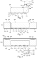
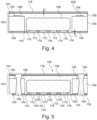
- Figure 1 to Figure 5 illustrate cross-sectional views of structures obtained during carrying out a method of manufacturing a component carrier with embedded component, shown in Figure 5 , according to an exemplary embodiment of the invention.
- a component carrier with layer stack and embedded component wherein the component has a redistribution layer with an electrically conductive pad protruding beyond the rest of the redistribution layer, preferably by not more than 30 ⁇ m. Therefore, the pads slightly protrude beyond the rest of the redistribution structure so as to ensure that they are not prone to bending or breakage during an assembly process.
- the protruding one or more pads may define spaces between dielectric redistribution structure material (for instance polyimide) and a lower main surface of the component carrier under production. Such gaps may be filled partially or entirely during lamination or adhesion of the component within the stack.
- components are provided with planar redistribution layer, i.e. without pads protruding beyond dielectric material of the redistribution layer.
- a temporary carrier such as an adhesive tape.
- the lower main surface of the obtained semi-finished component carrier is partially defined by the dielectric material of the redistribution layer.
- an exemplary embodiment of the invention provides a component carrier with redistribution structure having one or more pads protruding beyond dielectric material of the redistribution structure.
- one or more spaces remain between the at least one pad and the dielectric material of the redistribution structure.
- Such spaces may be filled with resin of a laminate (for instance prepreg) or by an electrically insulating filling adhesive used for gluing the component in the stack in place.
- electrically conductive material such as copper by electroless deposition without the need of sputtering. This may significantly simplify the manufacturing process.
- component embedding may be accomplished with elevated contact terminal design of the component to be embedded.
- a component contact laser via can be advantageously omitted. This may allow carrying out the manufacturing process with low effort and proper current carrying capability.
- an exemplary embodiment of the invention relates to an embedded-component-PCB (printed circuit board) and a corresponding manufacturing method which may advantageously involve sufficiently elevating electronic component's terminal(s) (for instance by minimum of 5 ⁇ m) beyond a planar dielectric surface of a redistribution structure formed on said component.
- Such a slight elevation of the component pad(s) or terminal(s) may be enough to realize a direct plating on the terminals and to avoid the significantly higher effort of a Ti or W-Ti sputtering process.
- RDL redistribution layer
- An exemplary embodiment of the invention may allow to manufacture a component carrier with embedded component with significantly reduced effort and processing complexity, as well as with an improved processing stability. Thus, it may be possible to reduce the manufacturing effort in comparison with a manufacturing process utilizing titanium sputtering on a polyimide layer without adding further complexity.
- the component 108 for instance embodied as a semiconductor chip, is provided with a redistribution structure 110 on its bottom side.
- the substantially planar redistribution structure 110 is provided at an exposed lower main surface thereof with a plurality of electrically conductive pads 112 which vertically protrude in a downward direction beyond a lower end surface 122 of dielectric material 114 of the redistribution structure 110.
- four pads 112 are provided at the face-down oriented component 108.
- any other number of pads 112 is possible as well.
- the component 108 can also have face-up pads (not shown). In this case, a direct full back side contact with a potential copper layer may be advantageous for heat management purposes.
- the component 108 may also have pads 112 on both opposing main surfaces thereof (not shown).
- the pads 112 protrude beyond the dielectric end surface 122 by not more than 30 ⁇ m.
- a total thickness D of the at least one pad 112 may be preferably in a range from 6 ⁇ m to 12 ⁇ m.
- An aspect ratio, i.e. a ratio between vertical thickness D and a horizontal diameter d of the respective pad 112 is preferably smaller than 0.2.
- the dielectric material 114 may comprise or consist of polyimide.
- the pads 112 may be made of copper.
- the component 108 is manufactured with thick copper pads 112 on redistribution structure 110 without polyimide coverage on free end faces 156 of the pads 112.
- the redistribution layer or structure 110 comprises dielectric material 114 (in particular made of polyimide) and pads 112 (in particular made of copper) extending downwardly beyond the dielectric end surface 122 of the dielectric material 114.
- dielectric material 114 in particular made of polyimide
- pads 112 in particular made of copper
- the properties (in particular thickness) of the pads 112 may be adjusted by plating.
- the component 108 In order to manufacture the illustrated component 108 with integrated redistribution structure 110 and downwardly protruding pads 112, it is possible to provide the component 108 with a preform of the redistribution structure 110 having a preform of the pads 112, in which preform the pads 112 flush or are aligned with the end surface 122 of the dielectric material 114 (not shown). Subsequently, the preform of the pads 11 may be selectively thickened by depositing additional metal on the preforms of the pads 112 until the pads 112 protrude beyond the end surface 122 to a desired extent.
- each protruding pad 112 may be a double layer pad or even a multilayer pad with at least three layers of metallic material.
- Each pad layer may be made of the same material (preferably copper), or different pad layers may be made of different materials. It is alternatively also possible that the pads 112 are single layer pads.
- the component 108 is placed in a cavity 158 formed in a layer stack 102.
- Stack 102 may be a plate shaped laminate type layer stack composed of a plurality of electrically conductive layer structures 104 and a plurality of electrically insulating layer structures 106.
- the electrically conductive layer structures 104 may comprise patterned copper foils and vertical through connections, for example copper filled laser vias.
- the electrically insulating layer structures 106 may comprise a resin (such as epoxy resin) and optionally reinforcing particles therein (for instance glass fibers or glass spheres).
- the electrically insulating layer structures 106 may be made of FR4 or ABF.
- the thick central electrically insulating layer structure 106 may be a fully cured core.
- the cavity 158 may be defined by a through-hole in the stack 102 which may be closed on a bottom side by attaching a temporary carrier 152 to a lower main surface of the stack 102.
- the temporary carrier 152 may for instance be a sticky tape.
- the component 108 has been embedded in the stack 102 and has been glued in place by lamination.
- the structure shown in Figure 3 can be obtained by laminating one or more further electrically insulating layer structures 106 and one or more further electrically conductive layer structures 104 to the upper main surface of the structure shown in Figure 2 .
- a prepreg layer (as further electrically insulating layer structure 106) and a copper foil (as further electrically conductive layer structure 104) may be laminated on top of the structure shown in Figure 2 .
- uncured material of the further electrically insulating layer structure 106 may become flowable or melt and may flow in gaps between stack 102, temporary carrier 152 and component 108, including gaps 154 described referring to Figure 1 .
- the filling medium in said gaps may become solid.
- underfill 118 material is formed in the gaps 154 by said now solidified resin material. This is shown in a detail 162 in Figure 3 . Detail 162 also shows that the bottom area formed by the free end faces 156 of the pads 112 and the bottom surface of the underfill 118 is aligned and forms a continuous planar surface.
- component 108 in place in the cavity 158 formed in stack 102 by filling liquid adhesive material in the gaps in between. Upon curing said adhesive material, the component 108 is again glued in place in cavity 158.
- the temporary carrier 152 may be removed.
- the temporary carrier 152 is a sticky tape, it may be simply peeled off from the lower main surface of the structure shown in Figure 3 .
- lower main surfaces of the stack 102, of the underfill 118 and of the pads 112 are at the same vertical level and form a common planar horizontal surface.
- their lower end surfaces are coplanar, aligned and in flush with each other.
- end surface 122 of the dielectric material 114 of the redistribution structure 110 is retracted upwardly and is no longer exposed.
- the underfill 118 here an underfilling laminate resin, is provided, inter alia, on the end surface 122 of dielectric material 114 between adjacent pads 112 of the electronic component 108.
- the material of the underfill 118 may be any kind of resin, for instance prepreg resin (in particular an epoxy resin), an epoxy derivative (such as Ajinomoto ® Build-up Film), etc.
- electrically conductive material 116 such as copper, may be applied on the entire upper and lower main surfaces of the structure shown in Figure 3 , including the exposed surface of the pads 112 and of the underfill 118. Said electrically conductive material 116 may be applied by electroless deposition followed by galvanic plating. In the shown embodiment, the electrically conductive material 116 is formed as continuous electrically conductive layers on the top and bottom main surfaces of the structure shown in Figure 3 . In particular, the electrically conductive layer structure 104 arranged on a bottom of the stack 102 is covered by said electrically conductive material 116. The electrically conductive material 116 is applied also on underfill 118 on the end surface 122 of the dielectric material 114 between adjacent pads 112 and laterally of the pads 112, as well as on the pads 112.
- the electrically conductive material 116 is formed on both opposing main surfaces of the structure shown in Figure 3 by electroless deposition. If the copper layer formed as electrically conductive material 116 by electroless plating shall be further thickened, it is possible to carry out subsequently a galvanic plating process until a desired thickness L of the continuous layer of electrically conductive material 116 is obtained.
- the electrically conductive material 116 is deposited for enabling the formation of desired lateral electric connections, which can be obtained by patterning the latter, as shown in Figure 5 . In other words, subsequent patterning (compare Figure 5 ) enables a circuit designer to freely design laterally electrically conductive connections.
- Said electric connections may thus be formed by plating, rather than by sputtering (which is more cumbersome). Since the poorly adhesive polyimide of the dielectric material 114 is no longer exposed due to its coverage by underfill 118, no adhesion issues occur when depositing the additional electrically conductive material 118 in particular on the underfill 118 and on the further electrically insulating layer structure 106 (for instance both epoxy resin) used for laminating, as described. Thickness L of the continuous layers of electrically conductive material 116 may be adjusted by adjusting the electroless deposition process (and optionally the galvanic plating process).
- the electrically conductive material 116 on the lower main surface of Figure 4 is patterned (for instance by lithographic etching) to form lands 124 on the pads 112. As can be seen, the lands 124 extend laterally beyond the respective pad 112. This enables a circuit designer to laterally extend the electrically conductive connections of component carrier 100 and thereby refine the electric connection.
- laser through holes have been formed extending vertically through the stack 102. Thereafter, the laser through holes have been filled with an electrically conductive filling medium, such as copper, to thereby form electrically conductive vertical interconnects 164 connecting a front side with a back side of the readily manufactured component carrier 100.
- an electrically conductive filling medium such as copper
- This component carrier 100 comprises stack 102 composed of electrically conductive layer structures 104 and electrically insulating layer structures 106.
- Component 108 is embedded in the stack 102.
- the component 108 comprises redistribution structure 110 with electrically conductive pads 112 vertically protruding beyond end surface 122 of dielectric material 114 of the redistribution structure 110 by not more than 30 ⁇ m. Patterned electrically conductive material 116 is applied on said pads 112 to thicken them.
- the electrically conductive material 116 can be deposited by electroless deposition not only on the material of the pads 112, but also on the resin underfill 118 in between. Due to the protrusion of the pads 112 beyond the end surfaces 122 of the dielectric material 114 of the redistribution structure 110, no polyimide surfaces are exposed when depositing the electrically conductive material 116 so that the formation of the electrically conductive material 116 also works on the underfill 118 with proper adhesion. As a result, sputtering may be made dispensable for forming electrically conductive material 116. Furthermore, a high reliability and an increased stability of the manufactured component carrier 100 may be achieved.
Landscapes
- Engineering & Computer Science (AREA)
- Microelectronics & Electronic Packaging (AREA)
- Manufacturing & Machinery (AREA)
- Production Of Multi-Layered Print Wiring Board (AREA)
Claims (13)
- Support de composant (100), dans lequel le support de composant (100) comprend :un empilement (102) comprenant au moins une structure de couche électroconductrice (104) et/ou au moins une structure de couche électriquement isolante (106) ;un composant (108) incorporé dans l'empilement (102),dans lequel le composant (108) comprend une structure de redistribution (110) présentant un matériau diélectrique (114) et au moins un plot électroconducteur faisant saillie verticalement (112),et un matériau électroconducteur (116) sur au moins une partie dudit au moins un plot électroconducteur (112) ;caractérisé en ce quela au moins une plot électroconducteur (112) fait saillie verticalement au-delà d'une surface d'extrémité (122) de matériau diélectrique (114) de la structure de redistribution (110) ;et caractérisé en outre parun sous-remplissage (118) sur la surface d'extrémité (122) du matériau diélectrique (114) et entre des plots électroconducteurs adjacents (112) du composant (108), dans lequel le matériau de sous-remplissage (118) entoure également au moins une partie des parois latérales et/ou au moins une partie d'une surface principale supérieure du composant incorporé (108) pour relier mécaniquement le composant (108) à l'empilement (102) ; etun matériau électroconducteur (116) également sur le sous-remplissage (118).
- Support de composant (100) selon la revendication 1, comprenant au moins l'une des caractéristiques suivantes :dans lequel le matériau diélectrique (114) comprend ou est constitué d'un matériau plaquable anélectrolytique ou faiblement électrolytique, en particulier du polyimide ou du polybenzoxazole ;dans lequel le sous-remplissage (118) est une résine stratifiée de sous-remplissage ;dans lequel le au moins un plot électroconducteur (112) fait saillie verticalement au-delà de la surface d'extrémité (122) d'au plus 30 µm ;dans lequel le matériau électroconducteur (116) est également appliqué sur la résine stratifiée de sous-remplissage sur la surface d'extrémité (122) du matériau diélectrique (114) et entre des plots électroconducteurs adjacents (112).
- Support de composant (100) selon la revendication 1 ou 2, dans lequel le matériau électroconducteur (116) comprend ou est constitué de cuivre.
- Support de composant (100) selon l'une quelconque des revendications 1 à 3, dans lequel une de la au moins une structure de couche électroconductrice (104) est agencée sur un fond de l'empilement (102) et est au moins partiellement recouverte par ledit matériau électroconducteur (116).
- Support de composant (100) selon l'une quelconque des revendications 1 à 4, comprenant au moins l'une des caractéristiques suivantes :dans lequel une épaisseur (D) du au moins un plot électroconducteur(112) est dans une plage allant de 4 µm à 30 µm, en particulier dans une plage allant de 4 µm à 20 µm, plus particulièrement dans une plage allant de 6 µm à 12 µm ;dans lequel un rapport entre une épaisseur (D) et un diamètre (d) du au moins une plot électroconducteur (112) est inférieur à 0,5, en particulier est inférieur à 0,2.
- Support de composant (100) selon l'une quelconque des revendications 1 à 5, dans lequel le matériau électroconducteur (116) est structuré pour former au moins une plage (124) sur le au moins un plot électroconducteur (112), dans lequel en particulier la au moins une plage (124) s'étend latéralement au-delà du au moins un plot électroconducteur (112) sur au moins un côté.
- Support de composant (100) selon l'une quelconque des revendications 1 à 6, dans lequel le matériau électroconducteur (116) fait partie d'une couche métallique structurée.
- Support de composant (100) selon l'une quelconque des revendications 1 à 7, comprenant au moins l'une des caractéristiques suivantes :dans lequel le composant (108) est sélectionné dans un groupe constitué d'un composant électronique, d'un insert électriquement non conducteur et/ou électriquement conducteur, d'une unité de transfert de chaleur, d'un élément de guidage de lumière, d'un élément optique, d'un pont, d'une unité de récupération d'énergie, d'un composant électronique actif, d'un composant électronique passif, d'une puce électronique, d'un dispositif de stockage, d'un filtre, d'un circuit intégré, d'un composant de traitement de signal, d'un composant de gestion de puissance, d'un élément d'interface optoélectronique, d'un convertisseur de tension, d'un composant cryptographique, d'un émetteur et/ou d'un récepteur, d'un transducteur électromécanique, d'un actionneur, d'un système microélectromécanique, d'un microprocesseur, d'un condensateur, d'une résistance, d'une inductance, d'un accumulateur, d'un commutateur, d'une caméra, d'une antenne, d'un élément magnétique, d'un support de composant supplémentaire (100) et d'une puce logique ;dans lequel la au moins une structure de couche électroconductrice (104) comprend au moins l'un du groupe constitué du cuivre, de l'aluminium, du nickel, de l'argent, de l'or, du palladium et du tungstène, l'un quelconque des matériaux mentionnés étant facultativement revêtu d'un matériau supra-conducteur tel que le graphène ;dans lequel la au moins une structure de couche électriquement isolante (106) comprend au moins un du groupe constitué de résine, en particulier de résine renforcée ou non renforcée, par exemple de résine époxy ou de résine de bismaléimide-triazine, de FR-4, de FR-5, d'ester de cyanate, de dérivé de polyphénylène, de verre, de matériau de préimprégné, de polyimide, de polyamide, de polymère à cristaux liquides, de film de recharge à base d'époxy, de polytétrafluoroéthylène, de céramique et d'oxyde métallique ; ;dans lequel le support de composant (100) est réalisé sous la forme d'une plaque ;dans lequel le support de composant (100) est configuré sous la forme de l'un du groupe constitué d'une carte de circuit imprimé, et d'un substrat ;configuré sous la forme d'un support de composant (100) de type stratifié.
- Procédé de fabrication d'un support de composant (100), dans lequel le procédé comprend les étapes consistant à :fournir un empilement (102) comprenant au moins une structure de couche électroconductrice (104) et/ou au moins une structure de couche électriquement isolante (106) ;incorporer un composant (108) dans l'empilement (102) ;fournir au composant (108) une structure de redistribution (110) présentant un matériau diélectrique (114) et au moins un plot électroconducteur faisant saillie verticalement (112), dans lequel le au moins une plot électroconducteur (112) fait saillie verticalement au-delà d'une surface d'extrémité (122) du matériau diélectrique (114) de la structure de redistribution (110),caractérisé par les étapes consistant àfournir un sous-remplissage (118) sur la surface d'extrémité (122) du matériau diélectrique (114) et entre des plots électroconducteurs adjacents (112) du composant (108), dans lequel le matériau de sous-remplissage (118) entoure également au moins une partie des parois latérales et/ou au moins une partie d'une surface principale supérieure du composant incorporé (108) pour relier mécaniquement le composant (108) à l'empilement (102) ; etformer un matériau électroconducteur (116) sur au moins une partie dudit au moins une plot électroconducteur (112) et sur le sous-remplissage (118).
- Procédé selon la revendication 9, dans lequel le procédé comprend une application du matériau électroconducteur (116) par placage anélectrolytique, facultativement suivi d'un placage galvanique.
- Procédé selon la revendication 9 ou 10, dans lequel le procédé comprend la formation du matériau électroconducteur (116) également sur une résine stratifiée de sous-remplissage, qui forme le sous-remplissage (118) et recouvre la surface d'extrémité (122) du matériau diélectrique (114) entre des plots électroconducteurs adjacents (112).
- Procédé selon l'une quelconque des revendications 9 à 11, dans lequel le procédé comprend la formation du matériau électroconducteur (116) sous la forme d'une couche continue,
en particulier dans lequel le procédé comprend la structuration subséquente de la couche continue pour former ainsi au moins une plage (124) connectée électriquement à au moins un plot électroconducteur (112). - Procédé selon l'une quelconque des revendications 9 à 12, dans lequel le procédé comprend en outre les étapes consistant à :fournir au composant (108) une préforme de la structure de redistribution (110) et une préforme du au moins un plot électroconducteur (112), en particulier en affleurement par rapport à la surface d'extrémité (122) du matériau diélectrique (114) ; etépaissir sélectivement la préforme du au moins une plot électroconducteur (112) de manière à faire saillie au-delà de la surface d'extrémité (122), en particulier en plaquant un métal supplémentaire sur la préforme du au moins un plot électroconducteur (112).
Applications Claiming Priority (1)
| Application Number | Priority Date | Filing Date | Title |
|---|---|---|---|
| CN201911272714.7A CN111564414B (zh) | 2019-12-12 | 2019-12-12 | 部件承载件及制造部件承载件的方法 |
Publications (2)
| Publication Number | Publication Date |
|---|---|
| EP3836209A1 EP3836209A1 (fr) | 2021-06-16 |
| EP3836209B1 true EP3836209B1 (fr) | 2024-04-24 |
Family
ID=72074082
Family Applications (1)
| Application Number | Title | Priority Date | Filing Date |
|---|---|---|---|
| EP20211200.9A Active EP3836209B1 (fr) | 2019-12-12 | 2020-12-02 | Support de composant et sa fabrication |
Country Status (3)
| Country | Link |
|---|---|
| US (1) | US11343916B2 (fr) |
| EP (1) | EP3836209B1 (fr) |
| CN (1) | CN111564414B (fr) |
Families Citing this family (6)
| Publication number | Priority date | Publication date | Assignee | Title |
|---|---|---|---|---|
| EP3557608A1 (fr) * | 2018-04-19 | 2019-10-23 | AT & S Austria Technologie & Systemtechnik Aktiengesellschaft | Circuit intégré avec fonctionnalité d'interposition et procédé de fabrication d'un tel circuit intégré |
| CN112201652A (zh) * | 2019-07-07 | 2021-01-08 | 深南电路股份有限公司 | 线路板及其制作方法 |
| CN114178710B (zh) * | 2020-08-24 | 2024-11-26 | 奥特斯(中国)有限公司 | 部件承载件及其制造方法 |
| CN114244055B (zh) * | 2022-01-11 | 2023-05-26 | 苏州昀冢电子科技股份有限公司 | 线圈组件及其使用该线圈组件的音圈马达 |
| TWI808716B (zh) * | 2022-04-08 | 2023-07-11 | 欣興電子股份有限公司 | 具有對接結構的電路板、電路板模組及電路板製造方法 |
| EP4307845A1 (fr) * | 2022-07-12 | 2024-01-17 | AT&S Austria Technologie & Systemtechnik Aktiengesellschaft | Support de composant doté d'une structure de couche de conception estampillée et composant intégré |
Family Cites Families (23)
| Publication number | Priority date | Publication date | Assignee | Title |
|---|---|---|---|---|
| JPH08134212A (ja) * | 1994-11-14 | 1996-05-28 | Hitachi Ltd | 配線構造体とその製造法 |
| US5773359A (en) * | 1995-12-26 | 1998-06-30 | Motorola, Inc. | Interconnect system and method of fabrication |
| CN100336426C (zh) * | 2000-02-25 | 2007-09-05 | 揖斐电株式会社 | 多层印刷电路板以及多层印刷电路板的制造方法 |
| US7618844B2 (en) * | 2005-08-18 | 2009-11-17 | Intelleflex Corporation | Method of packaging and interconnection of integrated circuits |
| US8024858B2 (en) * | 2008-02-14 | 2011-09-27 | Ibiden Co., Ltd. | Method of manufacturing printed wiring board with built-in electronic component |
| JP5262188B2 (ja) * | 2008-02-29 | 2013-08-14 | 富士通株式会社 | 基板 |
| JPWO2010038489A1 (ja) * | 2008-09-30 | 2012-03-01 | イビデン株式会社 | 電子部品内蔵配線板及びその製造方法 |
| US9627324B2 (en) | 2009-11-17 | 2017-04-18 | Evatec Ag | Apparatus and method for processing a substrate |
| US10373870B2 (en) * | 2010-02-16 | 2019-08-06 | Deca Technologies Inc. | Semiconductor device and method of packaging |
| US20130037929A1 (en) | 2011-08-09 | 2013-02-14 | Kay S. Essig | Stackable wafer level packages and related methods |
| JP6006523B2 (ja) * | 2012-04-27 | 2016-10-12 | 新光電気工業株式会社 | 接続構造体、配線基板ユニット、電子回路部品ユニット、及び電子装置 |
| US9209151B2 (en) * | 2013-09-26 | 2015-12-08 | General Electric Company | Embedded semiconductor device package and method of manufacturing thereof |
| US10079156B2 (en) | 2014-11-07 | 2018-09-18 | Advanced Semiconductor Engineering, Inc. | Semiconductor package including dielectric layers defining via holes extending to component pads |
| KR101780541B1 (ko) | 2015-03-24 | 2017-09-21 | 앰코 테크놀로지 코리아 주식회사 | 반도체 디바이스 및 그 제조 방법 |
| US10199337B2 (en) | 2015-05-11 | 2019-02-05 | Samsung Electro-Mechanics Co., Ltd. | Electronic component package and method of manufacturing the same |
| JP6534948B2 (ja) * | 2016-02-26 | 2019-06-26 | 信越化学工業株式会社 | 半導体装置の製造方法、フリップチップ型半導体装置の製造方法、半導体装置及びフリップチップ型半導体装置 |
| US20170373011A1 (en) | 2016-06-28 | 2017-12-28 | General Electric Company | Semiconductor die backside devices and methods of fabrication thereof |
| US10297471B2 (en) * | 2016-12-15 | 2019-05-21 | Taiwan Semiconductor Manufacturing Company, Ltd. | Fan-out structure and method of fabricating the same |
| CN108307591A (zh) * | 2017-01-13 | 2018-07-20 | 奥特斯奥地利科技与系统技术有限公司 | 通过在安装于部件承载件材料之前用附着物覆盖部件制造的部件承载件 |
| US10269728B2 (en) | 2017-06-30 | 2019-04-23 | Taiwan Semiconductor Manufacturing Company, Ltd. | Semiconductor device with shielding structure for cross-talk reduction |
| EP4531102A3 (fr) * | 2017-10-25 | 2025-07-02 | AT & S Austria Technologie & Systemtechnik Aktiengesellschaft | Composant d'enrobage avec pilier préconnecté dans un support de composant |
| EP3557608A1 (fr) | 2018-04-19 | 2019-10-23 | AT & S Austria Technologie & Systemtechnik Aktiengesellschaft | Circuit intégré avec fonctionnalité d'interposition et procédé de fabrication d'un tel circuit intégré |
| CN109640521B (zh) * | 2018-11-20 | 2020-06-30 | 奥特斯科技(重庆)有限公司 | 制造具有嵌入式集群的部件承载件的方法以及部件承载件 |
-
2019
- 2019-12-12 CN CN201911272714.7A patent/CN111564414B/zh active Active
-
2020
- 2020-12-02 EP EP20211200.9A patent/EP3836209B1/fr active Active
- 2020-12-02 US US17/247,174 patent/US11343916B2/en active Active
Also Published As
| Publication number | Publication date |
|---|---|
| EP3836209A1 (fr) | 2021-06-16 |
| US11343916B2 (en) | 2022-05-24 |
| US20210185816A1 (en) | 2021-06-17 |
| CN111564414B (zh) | 2021-09-24 |
| CN111564414A (zh) | 2020-08-21 |
Similar Documents
| Publication | Publication Date | Title |
|---|---|---|
| EP3836209B1 (fr) | Support de composant et sa fabrication | |
| US11810844B2 (en) | Component carrier and method of manufacturing the same | |
| US12400968B2 (en) | Component with dielectric layer for embedding in component carrier | |
| US10765005B2 (en) | Embedding component with pre-connected pillar in component carrier | |
| US11553599B2 (en) | Component carrier comprising pillars on a coreless substrate | |
| US11452212B2 (en) | Component carrier with electrically conductive layer structures having windows defined by a conformal mask and tapering at least partially | |
| US11700690B2 (en) | Component carrier with blind hole filled with an electrically conductive medium and fulfilling a minimum thickness design rule | |
| US11160165B2 (en) | Component carrier with through hole extending through multiple dielectric layers | |
| US11470714B2 (en) | Component carrier with embedded component and horizontally elongated via | |
| US11324122B2 (en) | Component carrier and method of manufacturing the same | |
| US11570905B2 (en) | Method of manufacturing component carrier and component carrier | |
| US11424179B2 (en) | Ultra-thin component carrier having high stiffness and method of manufacturing the same | |
| US12205877B2 (en) | Ultra-thin component carrier having high stiffness and method of manufacturing the same | |
| EP3846598A1 (fr) | Agencement doté d'un support central et de deux empilements de couche opposés, support de composant et procédé de fabrication | |
| US20240021440A1 (en) | Component Carrier and Method of Manufacturing the Same | |
| US20250071907A1 (en) | Component Carrier With Embedded Interposer Laterally Between Electrically Conductive Structures of Stack |
Legal Events
| Date | Code | Title | Description |
|---|---|---|---|
| PUAI | Public reference made under article 153(3) epc to a published international application that has entered the european phase |
Free format text: ORIGINAL CODE: 0009012 |
|
| STAA | Information on the status of an ep patent application or granted ep patent |
Free format text: STATUS: THE APPLICATION HAS BEEN PUBLISHED |
|
| AK | Designated contracting states |
Kind code of ref document: A1 Designated state(s): AL AT BE BG CH CY CZ DE DK EE ES FI FR GB GR HR HU IE IS IT LI LT LU LV MC MK MT NL NO PL PT RO RS SE SI SK SM TR |
|
| STAA | Information on the status of an ep patent application or granted ep patent |
Free format text: STATUS: REQUEST FOR EXAMINATION WAS MADE |
|
| 17P | Request for examination filed |
Effective date: 20210914 |
|
| RBV | Designated contracting states (corrected) |
Designated state(s): AL AT BE BG CH CY CZ DE DK EE ES FI FR GB GR HR HU IE IS IT LI LT LU LV MC MK MT NL NO PL PT RO RS SE SI SK SM TR |
|
| GRAP | Despatch of communication of intention to grant a patent |
Free format text: ORIGINAL CODE: EPIDOSNIGR1 |
|
| STAA | Information on the status of an ep patent application or granted ep patent |
Free format text: STATUS: GRANT OF PATENT IS INTENDED |
|
| INTG | Intention to grant announced |
Effective date: 20231219 |
|
| GRAS | Grant fee paid |
Free format text: ORIGINAL CODE: EPIDOSNIGR3 |
|
| GRAA | (expected) grant |
Free format text: ORIGINAL CODE: 0009210 |
|
| STAA | Information on the status of an ep patent application or granted ep patent |
Free format text: STATUS: THE PATENT HAS BEEN GRANTED |
|
| AK | Designated contracting states |
Kind code of ref document: B1 Designated state(s): AL AT BE BG CH CY CZ DE DK EE ES FI FR GB GR HR HU IE IS IT LI LT LU LV MC MK MT NL NO PL PT RO RS SE SI SK SM TR |
|
| REG | Reference to a national code |
Ref country code: GB Ref legal event code: FG4D |
|
| REG | Reference to a national code |
Ref country code: CH Ref legal event code: EP |
|
| REG | Reference to a national code |
Ref country code: DE Ref legal event code: R096 Ref document number: 602020029471 Country of ref document: DE |
|
| REG | Reference to a national code |
Ref country code: IE Ref legal event code: FG4D |
|
| P01 | Opt-out of the competence of the unified patent court (upc) registered |
Effective date: 20240510 |
|
| REG | Reference to a national code |
Ref country code: LT Ref legal event code: MG9D |
|
| REG | Reference to a national code |
Ref country code: NL Ref legal event code: MP Effective date: 20240424 |
|
| REG | Reference to a national code |
Ref country code: AT Ref legal event code: MK05 Ref document number: 1680581 Country of ref document: AT Kind code of ref document: T Effective date: 20240424 |
|
| PG25 | Lapsed in a contracting state [announced via postgrant information from national office to epo] |
Ref country code: NL Free format text: LAPSE BECAUSE OF FAILURE TO SUBMIT A TRANSLATION OF THE DESCRIPTION OR TO PAY THE FEE WITHIN THE PRESCRIBED TIME-LIMIT Effective date: 20240424 |
|
| PG25 | Lapsed in a contracting state [announced via postgrant information from national office to epo] |
Ref country code: NL Free format text: LAPSE BECAUSE OF FAILURE TO SUBMIT A TRANSLATION OF THE DESCRIPTION OR TO PAY THE FEE WITHIN THE PRESCRIBED TIME-LIMIT Effective date: 20240424 |
|
| PG25 | Lapsed in a contracting state [announced via postgrant information from national office to epo] |
Ref country code: IS Free format text: LAPSE BECAUSE OF FAILURE TO SUBMIT A TRANSLATION OF THE DESCRIPTION OR TO PAY THE FEE WITHIN THE PRESCRIBED TIME-LIMIT Effective date: 20240824 |
|
| PG25 | Lapsed in a contracting state [announced via postgrant information from national office to epo] |
Ref country code: BG Free format text: LAPSE BECAUSE OF FAILURE TO SUBMIT A TRANSLATION OF THE DESCRIPTION OR TO PAY THE FEE WITHIN THE PRESCRIBED TIME-LIMIT Effective date: 20240424 |
|
| PG25 | Lapsed in a contracting state [announced via postgrant information from national office to epo] |
Ref country code: FI Free format text: LAPSE BECAUSE OF FAILURE TO SUBMIT A TRANSLATION OF THE DESCRIPTION OR TO PAY THE FEE WITHIN THE PRESCRIBED TIME-LIMIT Effective date: 20240424 Ref country code: HR Free format text: LAPSE BECAUSE OF FAILURE TO SUBMIT A TRANSLATION OF THE DESCRIPTION OR TO PAY THE FEE WITHIN THE PRESCRIBED TIME-LIMIT Effective date: 20240424 |
|
| PG25 | Lapsed in a contracting state [announced via postgrant information from national office to epo] |
Ref country code: GR Free format text: LAPSE BECAUSE OF FAILURE TO SUBMIT A TRANSLATION OF THE DESCRIPTION OR TO PAY THE FEE WITHIN THE PRESCRIBED TIME-LIMIT Effective date: 20240725 |
|
| PG25 | Lapsed in a contracting state [announced via postgrant information from national office to epo] |
Ref country code: PT Free format text: LAPSE BECAUSE OF FAILURE TO SUBMIT A TRANSLATION OF THE DESCRIPTION OR TO PAY THE FEE WITHIN THE PRESCRIBED TIME-LIMIT Effective date: 20240826 |
|
| PG25 | Lapsed in a contracting state [announced via postgrant information from national office to epo] |
Ref country code: ES Free format text: LAPSE BECAUSE OF FAILURE TO SUBMIT A TRANSLATION OF THE DESCRIPTION OR TO PAY THE FEE WITHIN THE PRESCRIBED TIME-LIMIT Effective date: 20240424 |
|
| PG25 | Lapsed in a contracting state [announced via postgrant information from national office to epo] |
Ref country code: AT Free format text: LAPSE BECAUSE OF FAILURE TO SUBMIT A TRANSLATION OF THE DESCRIPTION OR TO PAY THE FEE WITHIN THE PRESCRIBED TIME-LIMIT Effective date: 20240424 |
|
| PG25 | Lapsed in a contracting state [announced via postgrant information from national office to epo] |
Ref country code: PL Free format text: LAPSE BECAUSE OF FAILURE TO SUBMIT A TRANSLATION OF THE DESCRIPTION OR TO PAY THE FEE WITHIN THE PRESCRIBED TIME-LIMIT Effective date: 20240424 |
|
| PG25 | Lapsed in a contracting state [announced via postgrant information from national office to epo] |
Ref country code: LV Free format text: LAPSE BECAUSE OF FAILURE TO SUBMIT A TRANSLATION OF THE DESCRIPTION OR TO PAY THE FEE WITHIN THE PRESCRIBED TIME-LIMIT Effective date: 20240424 |
|
| PG25 | Lapsed in a contracting state [announced via postgrant information from national office to epo] |
Ref country code: PT Free format text: LAPSE BECAUSE OF FAILURE TO SUBMIT A TRANSLATION OF THE DESCRIPTION OR TO PAY THE FEE WITHIN THE PRESCRIBED TIME-LIMIT Effective date: 20240826 Ref country code: PL Free format text: LAPSE BECAUSE OF FAILURE TO SUBMIT A TRANSLATION OF THE DESCRIPTION OR TO PAY THE FEE WITHIN THE PRESCRIBED TIME-LIMIT Effective date: 20240424 Ref country code: NO Free format text: LAPSE BECAUSE OF FAILURE TO SUBMIT A TRANSLATION OF THE DESCRIPTION OR TO PAY THE FEE WITHIN THE PRESCRIBED TIME-LIMIT Effective date: 20240724 Ref country code: LV Free format text: LAPSE BECAUSE OF FAILURE TO SUBMIT A TRANSLATION OF THE DESCRIPTION OR TO PAY THE FEE WITHIN THE PRESCRIBED TIME-LIMIT Effective date: 20240424 Ref country code: IS Free format text: LAPSE BECAUSE OF FAILURE TO SUBMIT A TRANSLATION OF THE DESCRIPTION OR TO PAY THE FEE WITHIN THE PRESCRIBED TIME-LIMIT Effective date: 20240824 Ref country code: HR Free format text: LAPSE BECAUSE OF FAILURE TO SUBMIT A TRANSLATION OF THE DESCRIPTION OR TO PAY THE FEE WITHIN THE PRESCRIBED TIME-LIMIT Effective date: 20240424 Ref country code: GR Free format text: LAPSE BECAUSE OF FAILURE TO SUBMIT A TRANSLATION OF THE DESCRIPTION OR TO PAY THE FEE WITHIN THE PRESCRIBED TIME-LIMIT Effective date: 20240725 Ref country code: FI Free format text: LAPSE BECAUSE OF FAILURE TO SUBMIT A TRANSLATION OF THE DESCRIPTION OR TO PAY THE FEE WITHIN THE PRESCRIBED TIME-LIMIT Effective date: 20240424 Ref country code: ES Free format text: LAPSE BECAUSE OF FAILURE TO SUBMIT A TRANSLATION OF THE DESCRIPTION OR TO PAY THE FEE WITHIN THE PRESCRIBED TIME-LIMIT Effective date: 20240424 Ref country code: BG Free format text: LAPSE BECAUSE OF FAILURE TO SUBMIT A TRANSLATION OF THE DESCRIPTION OR TO PAY THE FEE WITHIN THE PRESCRIBED TIME-LIMIT Effective date: 20240424 Ref country code: AT Free format text: LAPSE BECAUSE OF FAILURE TO SUBMIT A TRANSLATION OF THE DESCRIPTION OR TO PAY THE FEE WITHIN THE PRESCRIBED TIME-LIMIT Effective date: 20240424 Ref country code: RS Free format text: LAPSE BECAUSE OF FAILURE TO SUBMIT A TRANSLATION OF THE DESCRIPTION OR TO PAY THE FEE WITHIN THE PRESCRIBED TIME-LIMIT Effective date: 20240724 |
|
| PG25 | Lapsed in a contracting state [announced via postgrant information from national office to epo] |
Ref country code: DK Free format text: LAPSE BECAUSE OF FAILURE TO SUBMIT A TRANSLATION OF THE DESCRIPTION OR TO PAY THE FEE WITHIN THE PRESCRIBED TIME-LIMIT Effective date: 20240424 |
|
| PG25 | Lapsed in a contracting state [announced via postgrant information from national office to epo] |
Ref country code: EE Free format text: LAPSE BECAUSE OF FAILURE TO SUBMIT A TRANSLATION OF THE DESCRIPTION OR TO PAY THE FEE WITHIN THE PRESCRIBED TIME-LIMIT Effective date: 20240424 |
|
| PG25 | Lapsed in a contracting state [announced via postgrant information from national office to epo] |
Ref country code: CZ Free format text: LAPSE BECAUSE OF FAILURE TO SUBMIT A TRANSLATION OF THE DESCRIPTION OR TO PAY THE FEE WITHIN THE PRESCRIBED TIME-LIMIT Effective date: 20240424 |
|
| PG25 | Lapsed in a contracting state [announced via postgrant information from national office to epo] |
Ref country code: RO Free format text: LAPSE BECAUSE OF FAILURE TO SUBMIT A TRANSLATION OF THE DESCRIPTION OR TO PAY THE FEE WITHIN THE PRESCRIBED TIME-LIMIT Effective date: 20240424 Ref country code: SK Free format text: LAPSE BECAUSE OF FAILURE TO SUBMIT A TRANSLATION OF THE DESCRIPTION OR TO PAY THE FEE WITHIN THE PRESCRIBED TIME-LIMIT Effective date: 20240424 |
|
| REG | Reference to a national code |
Ref country code: DE Ref legal event code: R097 Ref document number: 602020029471 Country of ref document: DE |
|
| PG25 | Lapsed in a contracting state [announced via postgrant information from national office to epo] |
Ref country code: SM Free format text: LAPSE BECAUSE OF FAILURE TO SUBMIT A TRANSLATION OF THE DESCRIPTION OR TO PAY THE FEE WITHIN THE PRESCRIBED TIME-LIMIT Effective date: 20240424 |
|
| PG25 | Lapsed in a contracting state [announced via postgrant information from national office to epo] |
Ref country code: SM Free format text: LAPSE BECAUSE OF FAILURE TO SUBMIT A TRANSLATION OF THE DESCRIPTION OR TO PAY THE FEE WITHIN THE PRESCRIBED TIME-LIMIT Effective date: 20240424 Ref country code: SK Free format text: LAPSE BECAUSE OF FAILURE TO SUBMIT A TRANSLATION OF THE DESCRIPTION OR TO PAY THE FEE WITHIN THE PRESCRIBED TIME-LIMIT Effective date: 20240424 Ref country code: RO Free format text: LAPSE BECAUSE OF FAILURE TO SUBMIT A TRANSLATION OF THE DESCRIPTION OR TO PAY THE FEE WITHIN THE PRESCRIBED TIME-LIMIT Effective date: 20240424 Ref country code: EE Free format text: LAPSE BECAUSE OF FAILURE TO SUBMIT A TRANSLATION OF THE DESCRIPTION OR TO PAY THE FEE WITHIN THE PRESCRIBED TIME-LIMIT Effective date: 20240424 Ref country code: DK Free format text: LAPSE BECAUSE OF FAILURE TO SUBMIT A TRANSLATION OF THE DESCRIPTION OR TO PAY THE FEE WITHIN THE PRESCRIBED TIME-LIMIT Effective date: 20240424 Ref country code: CZ Free format text: LAPSE BECAUSE OF FAILURE TO SUBMIT A TRANSLATION OF THE DESCRIPTION OR TO PAY THE FEE WITHIN THE PRESCRIBED TIME-LIMIT Effective date: 20240424 |
|
| PLBE | No opposition filed within time limit |
Free format text: ORIGINAL CODE: 0009261 |
|
| STAA | Information on the status of an ep patent application or granted ep patent |
Free format text: STATUS: NO OPPOSITION FILED WITHIN TIME LIMIT |
|
| 26N | No opposition filed |
Effective date: 20250127 |
|
| PG25 | Lapsed in a contracting state [announced via postgrant information from national office to epo] |
Ref country code: SI Free format text: LAPSE BECAUSE OF FAILURE TO SUBMIT A TRANSLATION OF THE DESCRIPTION OR TO PAY THE FEE WITHIN THE PRESCRIBED TIME-LIMIT Effective date: 20240424 |
|
| PG25 | Lapsed in a contracting state [announced via postgrant information from national office to epo] |
Ref country code: MC Free format text: LAPSE BECAUSE OF FAILURE TO SUBMIT A TRANSLATION OF THE DESCRIPTION OR TO PAY THE FEE WITHIN THE PRESCRIBED TIME-LIMIT Effective date: 20240424 |
|
| REG | Reference to a national code |
Ref country code: CH Ref legal event code: PL |
|
| PG25 | Lapsed in a contracting state [announced via postgrant information from national office to epo] |
Ref country code: LU Free format text: LAPSE BECAUSE OF NON-PAYMENT OF DUE FEES Effective date: 20241202 |
|
| GBPC | Gb: european patent ceased through non-payment of renewal fee |
Effective date: 20241202 |
|
| PG25 | Lapsed in a contracting state [announced via postgrant information from national office to epo] |
Ref country code: SE Free format text: LAPSE BECAUSE OF FAILURE TO SUBMIT A TRANSLATION OF THE DESCRIPTION OR TO PAY THE FEE WITHIN THE PRESCRIBED TIME-LIMIT Effective date: 20240424 |
|
| REG | Reference to a national code |
Ref country code: BE Ref legal event code: MM Effective date: 20241231 |
|
| PG25 | Lapsed in a contracting state [announced via postgrant information from national office to epo] |
Ref country code: GB Free format text: LAPSE BECAUSE OF NON-PAYMENT OF DUE FEES Effective date: 20241202 Ref country code: BE Free format text: LAPSE BECAUSE OF NON-PAYMENT OF DUE FEES Effective date: 20241231 |
|
| PG25 | Lapsed in a contracting state [announced via postgrant information from national office to epo] |
Ref country code: CH Free format text: LAPSE BECAUSE OF NON-PAYMENT OF DUE FEES Effective date: 20241231 |
|
| PG25 | Lapsed in a contracting state [announced via postgrant information from national office to epo] |
Ref country code: IE Free format text: LAPSE BECAUSE OF NON-PAYMENT OF DUE FEES Effective date: 20241202 |
|
| REG | Reference to a national code |
Ref country code: DE Ref legal event code: R079 Ref document number: 602020029471 Country of ref document: DE Free format text: PREVIOUS MAIN CLASS: H01L0023538000 Ipc: H10W0070600000 |
|
| PGFP | Annual fee paid to national office [announced via postgrant information from national office to epo] |
Ref country code: DE Payment date: 20251216 Year of fee payment: 6 |
|
| PGFP | Annual fee paid to national office [announced via postgrant information from national office to epo] |
Ref country code: FR Payment date: 20251229 Year of fee payment: 6 |
|
| PG25 | Lapsed in a contracting state [announced via postgrant information from national office to epo] |
Ref country code: IT Free format text: LAPSE BECAUSE OF FAILURE TO SUBMIT A TRANSLATION OF THE DESCRIPTION OR TO PAY THE FEE WITHIN THE PRESCRIBED TIME-LIMIT Effective date: 20240424 |
|
| PG25 | Lapsed in a contracting state [announced via postgrant information from national office to epo] |
Ref country code: CY Free format text: LAPSE BECAUSE OF FAILURE TO SUBMIT A TRANSLATION OF THE DESCRIPTION OR TO PAY THE FEE WITHIN THE PRESCRIBED TIME-LIMIT; INVALID AB INITIO Effective date: 20201202 |