EP3839103A1 - Kobaltfüllung von verbindungen in der mikroelektronik - Google Patents
Kobaltfüllung von verbindungen in der mikroelektronik Download PDFInfo
- Publication number
- EP3839103A1 EP3839103A1 EP21155629.5A EP21155629A EP3839103A1 EP 3839103 A1 EP3839103 A1 EP 3839103A1 EP 21155629 A EP21155629 A EP 21155629A EP 3839103 A1 EP3839103 A1 EP 3839103A1
- Authority
- EP
- European Patent Office
- Prior art keywords
- composition
- cobalt
- set forth
- ions
- submicron
- Prior art date
- Legal status (The legal status is an assumption and is not a legal conclusion. Google has not performed a legal analysis and makes no representation as to the accuracy of the status listed.)
- Granted
Links
Images
Classifications
-
- C—CHEMISTRY; METALLURGY
- C25—ELECTROLYTIC OR ELECTROPHORETIC PROCESSES; APPARATUS THEREFOR
- C25D—PROCESSES FOR THE ELECTROLYTIC OR ELECTROPHORETIC PRODUCTION OF COATINGS; ELECTROFORMING; APPARATUS THEREFOR
- C25D7/00—Electroplating characterised by the article coated
- C25D7/12—Semiconductors
- C25D7/123—Semiconductors first coated with a seed layer or a conductive layer
-
- C—CHEMISTRY; METALLURGY
- C25—ELECTROLYTIC OR ELECTROPHORETIC PROCESSES; APPARATUS THEREFOR
- C25D—PROCESSES FOR THE ELECTROLYTIC OR ELECTROPHORETIC PRODUCTION OF COATINGS; ELECTROFORMING; APPARATUS THEREFOR
- C25D3/00—Electroplating: Baths therefor
- C25D3/02—Electroplating: Baths therefor from solutions
- C25D3/12—Electroplating: Baths therefor from solutions of nickel or cobalt
- C25D3/14—Electroplating: Baths therefor from solutions of nickel or cobalt from baths containing acetylenic or heterocyclic compounds
- C25D3/16—Acetylenic compounds
-
- C—CHEMISTRY; METALLURGY
- C25—ELECTROLYTIC OR ELECTROPHORETIC PROCESSES; APPARATUS THEREFOR
- C25D—PROCESSES FOR THE ELECTROLYTIC OR ELECTROPHORETIC PRODUCTION OF COATINGS; ELECTROFORMING; APPARATUS THEREFOR
- C25D3/00—Electroplating: Baths therefor
- C25D3/02—Electroplating: Baths therefor from solutions
- C25D3/56—Electroplating: Baths therefor from solutions of alloys
- C25D3/562—Electroplating: Baths therefor from solutions of alloys containing more than 50% by weight of iron or nickel or cobalt
-
- C—CHEMISTRY; METALLURGY
- C25—ELECTROLYTIC OR ELECTROPHORETIC PROCESSES; APPARATUS THEREFOR
- C25D—PROCESSES FOR THE ELECTROLYTIC OR ELECTROPHORETIC PRODUCTION OF COATINGS; ELECTROFORMING; APPARATUS THEREFOR
- C25D5/00—Electroplating characterised by the process; Pretreatment or after-treatment of workpieces
- C25D5/18—Electroplating using modulated, pulsed or reversing current
Definitions
- compositions and processes described herein generally relate to electrolytic deposition chemistry and a method for depositing cobalt and cobalt alloys; and more specifically to additives and overall compositions for use in an electrolytic plating solution and a method for cobalt-based metallization of interconnect features in semiconductor substrates.
- electrical interconnects are formed in an integrated circuit substrate by metal-filling of interconnect features such as vias and trenches formed in the substrate.
- Copper is a preferred conductor for electronic circuits. But when copper is deposited on a silicon substrate, it can diffuse rapidly into both the substrate and dielectric films such as SiO 2 or low k dielectrics. Copper also has a tendency to migrate from one location to another when electrical current passes through interconnect features in service, creating voids and hillocks. Copper can also diffuse into a device layer built on top of a substrate in multilayer device applications. Such diffusion can be detrimental to the device because it can damage an adjacent interconnect line and/or cause electrical leakage between two interconnects resulting in an electrical short. And the corresponding diffusion out of the interconnect feature can disrupt electrical flow.
- barrier layer On the walls of the cavity to prevent the diffusion and electromigration of copper into the surrounding silicon or dielectric structure.
- a seed layer is deposited over the barrier layer.
- the thickness of barrier and seed layers can be very small, especially where the electroplating solution contains a proper formulation of accelerators, suppressors, and levelers.
- the entry dimensions of vias and trenches become ever smaller, even the very thin barrier and seed layers progressively occupy higher and higher fractions of the entry dimensions.
- the entry apertures reach dimensions below 50 nm, and especially as they are further reduced to less than 40 nm, 30 nm, 20 nm or even less than 10 nm, such as about 8 or 9 nm, it becomes increasingly difficult to fill the cavity with a copper deposit that is entirely free of voids and seams.
- the most advanced features under current development have bottom widths of only 2-3 nm, a middle width of about, 4 nm, and a depth of 100 to 150 nm, translating to an aspect ratio of between about 25:1 and about 50:1.
- Electrolytic deposition of Co is performed in a variety of applications in the manufacture of microelectronic devices.
- Co is used in capping of damascene Cu metallization employed to form electrical interconnects in integrated circuit substrates.
- damascene Cu metallization employed to form electrical interconnects in integrated circuit substrates.
- cobalt deposits because of a higher resistivity of cobalt deposits, such processes have not previously offered a satisfactory alternative to electrodeposition of copper in filling vias or trenches to provide the primary interconnect structures.
- compositions for the electrolytic deposition of cobalt comprising a source of cobalt ions; an accelerator compound; a suppressor compound; a buffering agent; and water.
- compositions are used in a process for filling a submicron cavity in a dielectric material wherein the cavity has a wall region comprising a contact material, the process comprising contacting a dielectric material comprising the cavity with an electrolytic cobalt plating composition under conditions effective for reduction of cobalt ions and deposit of cobalt on the wall regions, wherein the cobalt plating composition comprises a source of cobalt ions; an accelerator comprising an organic sulfur compound; an acetylenic suppressor compound; a buffering agent; and water.
- the composition may further include a compound that functions as a stress reducer.
- compositions for the electrodeposition of cobalt that are substantially free of divalent sulfur compounds, and preferably free of any compound that would function as an accelerator in superfilling of submicron features of a semiconductor integrated circuit device.
- These compositions comprise a source of cobalt ions, an acetylenic suppressor compound, a buffering agent and water.
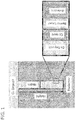
- Figure 1 is a schematic illustration of a cobalt filled feature prepared by the method of the invention.
- Cobalt-based electrolytic plating compositions and methods have been developed for use in electrolytic deposition of cobalt as an alternative to copper in the manufacture of semiconductor integrated circuit devices. More particularly, the compositions and methods of the invention are effective for filling submicron features of such devices.
- the cobalt-based plating compositions described herein contain a source of cobalt ions. Although various cobaltous salts can be used, CoSO 4 is highly preferred. This source of cobaltous ions is readily available, for example, as cobalt sulfate heptahydrate.
- the composition is formulated with a cobalt salt in a concentration which is sufficient to provide between about 1 and about 50 g/L of Co 2+ ions, such as between about 2 and about 10 g/L,or more preferably between about 5 and about 10 g/L.
- the composition also preferably contains one or more sulfidic accelerator compounds. While various organic sulfur compounds can be used, bis(sodium sulfopropyl)disulfide (“SPS”), 3-mercaptosulfonic acid (“MPS”), 3-(N,N-Dimethylthiocarbamoyl)-1-propane sulfonic acid sodium salt (“DPS”) and/or a thiourea-based compound are preferred. It has been found that a relatively strong accelerator provides for more effective superfilling of submicron cavities with cobalt. Thus, SPS and DPS are preferred accelerators, with SPS being particularly preferred.
- the concentration of the accelerator is preferably between about 0.5 and about 50 mg/L, such as between about 5 and about 25 mg/L.
- the composition also contains one or more suppressor compounds which preferably comprise acetylenic alcohol compounds or derivatives thereof.
- a currently preferred suppressor is propargyl alcohol.
- Other currently preferred suppressor compounds include ethoxylated propargyl alcohols, the product of the reaction of ethoxylated propargyl alcohol and 1,4-butanediol diglycidyl ether; propargyl alcohol; diethylene glycol bis(2-propynyl) ether; 1,4-bis(2-hydroxyethoxy)-2-butyne; and 2-butyne-1,4-diol.
- the concentration of the suppressor is preferably between about 5 and about 250 mg/L, such as between about 10 and about 50 mg/L.
- the cobalt electrodeposition composition also preferably comprises a buffer to stabilize the pH.
- a preferred buffer is boric acid.
- Boric acid (H 3 BO 3 ) may be incorporated into the composition in a concentration between about 5 and about 50 g/L, such as between about 15 and about 40 g/L.
- the pH of the composition is preferably in the range of about 1.5 to about 7, such as from about 2.5 to about 5.
- the electrodeposition composition is preferably free of nickel ions and iron ions. If either nickel ions or iron ions are present, the molar ratio of both nickel ions and iron ions, and the sum of nickel ions and iron ions, to cobalt ions is preferably not greater than about 0.01, or between about 0.00001 and about 0.01.
- the electrodeposition composition is also preferably substantially free of copper ions. Although very minor copper contamination may be difficult to avoid, it is particularly preferred that the copper ion content of the bath is no more than 20 ppb, e.g., in the range of 0.1 ppb to 20 ppb.
- the composition preferably consists essentially of an aqueous solution that is devoid of any solid particulates or other solid phase component.
- Particulate solids in a concentration up to 0.001 vol.%, preferably no more than 0.00001 vol.%, might be present due to infiltration of solids from process equipment, conduits or material sources, but the composition should, if possible, be free of any functional concentration of particulates, and most preferably entirely free of any solid particulates that would be detectable by analytical apparatus or methods commonly used in industrial fabrication of electronics products.
- the electrodeposition composition is preferably free of any functional concentration of reducing agents effective to reduce cobaltous ion (Co 2+ ) to metallic cobalt (Co 0 ).
- a functional concentration is meant any concentration of an agent that either is effective to reduce cobaltous ions in the absence of electrolytic current or is activated by an electrolytic current or electrolytic field to react with cobaltous ions.
- the electrodeposition composition may be used in a process for filling submicron features of a semiconductor base structure, the features comprising cavities in the base structure that are superfilled by rapid bottom-up deposition of cobalt.
- a metalizing substrate comprising a seminal conductive layer is formed on the internal surfaces of the submicron features, e.g., by physical vapor deposition of metal seed layer, preferably a cobalt metal seed layer, or deposition of a thin conductive polymer layer,
- a submicron electrical interconnect feature has a bottom, sidewalls, and top opening. The metalizing substrate is applied to the bottom and sidewall, and typically to the field surrounding the feature.
- the metalizing substrate within the feature is contacted with the electrodeposition composition and current is supplied to the electrodeposition composition to cause electrodeposition of cobalt that fills the submicron features.
- a vertical polarization gradient is formed in the feature which causes it to be filled by bottom up deposition at a rate of growth in the vertical direction which is greater than a rate of growth in the horizontal direction, yielding a cobalt interconnect that is substantially free of voids and other defects.
- an electrolytic circuit comprising the metalizing substrate, an anode, the aqueous electrodeposition composition, and a power source having a positive terminal in electrically conductive communication with the anode and a negative terminal in electrically conductive communication with the metalizing substrate.
- the metalizing substrate is immersed in the electrodeposition composition.
- An electrolytic current is delivered from the power source to the electrolytic composition in the circuit, thereby depositing cobalt on the metalizing substrate.
- the electrodeposition process is preferably conducted at a bath temperature in the range of about 5°C to about 80°C, more preferably between about 20°C and about 50°C, and a current density in the range between about 0.01 and about 2 A/dm 2 , preferably between about 0.05 and about 1 A/dm 2 .
- the current may be pulsed, which can provide some improvement in the uniformity of the deposit.
- On/off pulses and reverse pulses can be used. Pulse plating may enable relatively high current densities, e.g., >8 mA/cm 2 during cobalt deposition.
- the electrodeposition composition preferably includes a stress reducer such as saccharin.
- a stress reducer such as saccharin.
- saccharin is present in the electrodeposition composition in a concentration between about 10 and about 300 ppm, more preferably between about 100 and about 200 ppm.
- internal tensile stresses in the cobalt deposit can range as high as 1000 MPa, typically between about 500 and about 800 Mpa.
- internal tensile stress in the cobalt deposit is no greater than 500 MPa, typically between 0 and about 500 MPa, more typically between 0 and about 400 MPa.
- the electrodeposition composition contains between about 0.1 and about 5 wt.% cobalt ions, between about 0.5 and about 50 mg/l accelerator; between about 5 and about 250 mg/l of an acetylenic suppressor compound; and between about 1 and about 4.5 wt.% buffer.
- the pH of the composition is preferably between about 1.5 and about 7, more preferably between about 2.5 and about 5.
- the electrodeposition composition contains between about 5 and about 10 g/l cobaltous ion, between about 5 and about 25 mg/l SPS, between about 5 and about 30 mg/l of a suppressor selected from the group consisting of propargyl alcohol and ethoxylated propargyl alcohol, the balance substantially water.
- the pH is preferably adjusted to a value between about 2.5 and about 3.5. Sulfuric acid is preferred for pH adjustment.
- the novel compositions and processes are effective in the preparation of semiconductor integrated circuit devices comprising the semiconductor base structure and submicron interconnect features filled with cobalt.
- Providing cobalt interconnects is especially advantageous where the interconnects have a width or diameter less than 100 nm and an aspect ratio of greater than 3:1.
- the attractiveness of cobalt increases as the size of the interconnect cavity decreases to 50 nm, 30 nm or below having aspect ratios of greater than 3:1, such as between 4:1 and 10:1 or higher.
- the process may be implemented to produce a semiconductor integrated circuit device comprising a semiconductor base structure having a plurality of cavities therein wherein each cavity of such plurality of cavities has a width or diameter of not greater than 20 nm and is filled with cobalt by electrodeposition over a seminal conductive layer of a given thickness on the interior wall of the cavity.
- Cavities can be filled having entry dimensions (width or diameter) as small as 7 nm or even 4 nm and aspect ratios of greater than 15:1, greater than 20:1 or even greater than 30:1, for example, between 10:1 and 50:1, or between 15:1 and 50:1.
- the volume of cobalt with which a via or trench having a width or diameter of 20 nm or less may be filled substantially exceeds the volume of copper with which the same feature may be filled.
- the volume of cobalt including, e.g., a 20 angstrom seed layer
- the volume of cobalt typically exceeds the volume of copper (also including a 20 angstrom seed layer) with which the same feature may be filled by at least 50%, more typically at least 100%.
- the relative difference increases as the size of the feature is further decreased.
- compositions and processes described herein enable formation of a cobalt filling having an electrical resistance that is competitive with copper.
- a cavity having a width or diameter (entry dimension) less than 15 nm may be filled with cobalt over a seminal conductive layer of a given thickness on an interior wall of the cavity in such volume that the cobalt filling has an electrical resistance not more than 20% greater than a reference filling provided by electrodeposition of copper over a seminal conductive layer of the same given thickness on the interior wall of a reference cavity of the same entry dimension as the cobalt filled cavity, wherein a barrier layer against copper diffusion underlies the seminal conductive layer in the reference cavity.
- the thickness of the barrier layer may be at least 30 angstroms.
- the electrical resistance of the cobalt filling can be significantly less than the electrical resistance of the reference copper filling.
- the utility of the cobalt filling as measured by its resistance relative to a copper filling becomes most pronounced in features having a width or diameter not greater than 10 nm, or not greater than 7 nm.
- the advantages provide by filling submicron interconnects with cobalt rather than copper can be illustrated by reference to the schematic drawing.
- the narrow width of the via or trench is necessarily further narrowed by the need to provide a seminal conductive layer for electrodeposition of the metal that fills the interconnect feature.
- the available space within the feature is further diminished by the barrier layer indicated in the schematic, which is necessary to prevent diffusion of copper into the semiconductor substrate.
- the barrier layer can be dispensed with, thereby materially increasing the volume available to be filled with metal.
- a cobalt seed layer can typically be 0.5 to 40 nm thick, but for features having a width below 15 nm, it has been found feasible to provide a cobalt seed layer having a thickness of only about 2 nm at the side wall, about 4nm at the bottom, and about 10 nm on the upper field surrounding the interconnect feature.
- a barrier layer can often be dispensed with where a submicron feature is to be filled with cobalt.
- a barrier layer can be very thin, e.g., 0.1 to 40 nm, such as about 1 nm on the sidewall, about 4 nm at the bottom, and about 10 nm on the field, thus preserving a maximum volume for the cobalt fill.
- Figure 1 shows a cobalt fill and deposit into a submicron feature having the space between the cobalt fill and the dielectric occupied by the metal seed layer which provides the seminal conductive layer for electrodeposition, and the optional barrier layer.
- the barrier layer is essential where the feature is filled with copper, but not necessary where the feature is filled with cobalt in accordance with this invention.
- a preferred product of the novel process comprises a semiconductor integrated circuit device comprising a semiconductor base structure having a plurality of cavities therein wherein each cavity of such plurality of cavities has an entry dimension of not greater than 15 nm and is filled with cobalt over a seminal conductive layer of a given thickness on the interior wall of the cavity, e.g., at least 20 angstroms.
- the electrical resistance of the cobalt filling is not more than 20% greater than a reference filling provided by electrodeposition of copper over a seminal conductive layer of the same given thickness located over a barrier layer on the interior wall of a reference cavity of the same entry dimension, the barrier layer typically having a thickness of at least 30 angstroms.
- each cavity of the plurality of cavities has an entry dimension of not greater than 12 nm, not greater than 9 nm, not greater than 8 nm, not greater than 7 nm or not greater than 4 nm, or between about 5 nm and about 15 nm.
- the aspect ratio of the cavities of the plurality of cavities is at least about 3:1, at least about 4:1, at least about 15:1, at least about 20:1 or at least about 30:1, typically between about 10:1 and about 50:1.
- the electrical resistance of the cobalt filling is equal to or less than the resistance of the reference copper filling.
- Internal tensile stress in the cobalt filling is not greater than 500 MPa, typically between about 0 and about 500 MPa, or between 0 and about 400 MPa.
- compositions and processes described above have been found highly satisfactory for superfilling submicron features of semiconductor integrated circuit devices with cobalt, it has been found that additional benefits can in some instances be achieved by limiting the divalent sulfur content of the plating bath. Where divalent sulfur compounds are substantially excluded from the plating bath, the sulfur content of the cobalt deposit is lowered, with consequent beneficial effects on chemical mechanical polishing and circuit performance.
- the composition may be considered "substantially free" of divalent sulfur compounds if it satisfies one or more of the following criteria: (i) submicron features of a semiconductor substrate are filled from the electrodeposition composition with a cobalt deposit that does not contain more than 300 ppm sulfur; or (ii) the concentration in the plating solution of accelerators comprising divalent sulfur is not greater than 1 mg/l. In this alternative embodiment, the concentration of compounds containing divalent sulfur atoms is not greater than 0.1 mg/l. Still more preferably, the concentration of compounds that contain divalent sulfur atoms is below the detection level using analytical techniques common to electronic product fabrication facilities.
- the electrodeposition composition is substantially free of compounds that contain sulfonic acid or sulfonate ion groups.
- the divalent sulfur-free compositions can contain saccharin as a stress reducer. Saccharin contributes only minimally, if at all, to the sulfur content of the cobalt deposit. It has been found that electrodeposition from compositions that contain no divalent sulfur compounds forms deposits that typically have a sulfur content no higher than about 300 ppm, typically 10 to 200 ppm, even where the electrodeposition composition comprises saccharin as a stress reducer.
- the divalent sulfur-free electrodeposition composition contains between about 0.1 and about 5 wt. % cobalt ions, between about 5 and about 250 mg/l suppressor compound; and between about 1 and about 4.5 wt.% buffer.
- the pH of the composition is preferably between about 1.5 and about 7, preferably between about 2.5 and about 5.
- the composition comprises between about 5 and about 10 g/L cobaltous ion, between about 5 and about 30 mg/L of a suppressor selected from the group consisting of propargyl alcohol and ethoxylated propargyl alcohol, the balance essentially water.
- the pH of such composition is preferably between about 2.5 and about 3.5.
- the composition is preferably substantially free of reducing agents, Ni ions and Fe ions.
- reducing agents Ni ions and Fe ions.
- the limitations on these components as described above with respect to plating baths containing organic sulfur compound accelerators apply equally to the compositions that exclude divalent sulfur compounds.
- An electrolytic cobalt deposition composition was prepared with the following components:
- This composition may be used to fill a feature having a 12 nm top opening, a 7 nm middle width, a 2 nm bottom width, and a depth of 130 nm at a current density of 4 mA/cm 2 for 3 minutes at room temperature and a rotation rate of 100 rpm.
Landscapes
- Chemical & Material Sciences (AREA)
- Organic Chemistry (AREA)
- Chemical Kinetics & Catalysis (AREA)
- Electrochemistry (AREA)
- Materials Engineering (AREA)
- Metallurgy (AREA)
- Engineering & Computer Science (AREA)
- Electroplating And Plating Baths Therefor (AREA)
- Electrodes Of Semiconductors (AREA)
- Electroplating Methods And Accessories (AREA)
- Polymers With Sulfur, Phosphorus Or Metals In The Main Chain (AREA)
- Organic Low-Molecular-Weight Compounds And Preparation Thereof (AREA)
- Catalysts (AREA)
Applications Claiming Priority (3)
| Application Number | Priority Date | Filing Date | Title |
|---|---|---|---|
| US201562186978P | 2015-06-30 | 2015-06-30 | |
| EP16744598.0A EP3317437B1 (de) | 2015-06-30 | 2016-06-30 | Kobaltfüllung von verbindungen in der mikroelektronik |
| PCT/US2016/040501 WO2017004424A1 (en) | 2015-06-30 | 2016-06-30 | Cobalt filling of interconnects in microelectronics |
Related Parent Applications (2)
| Application Number | Title | Priority Date | Filing Date |
|---|---|---|---|
| EP16744598.0A Division-Into EP3317437B1 (de) | 2015-06-30 | 2016-06-30 | Kobaltfüllung von verbindungen in der mikroelektronik |
| EP16744598.0A Division EP3317437B1 (de) | 2015-06-30 | 2016-06-30 | Kobaltfüllung von verbindungen in der mikroelektronik |
Publications (2)
| Publication Number | Publication Date |
|---|---|
| EP3839103A1 true EP3839103A1 (de) | 2021-06-23 |
| EP3839103B1 EP3839103B1 (de) | 2023-07-19 |
Family
ID=56550974
Family Applications (2)
| Application Number | Title | Priority Date | Filing Date |
|---|---|---|---|
| EP21155629.5A Active EP3839103B1 (de) | 2015-06-30 | 2016-06-30 | Kobaltfüllung von verbindungen in der mikroelektronik |
| EP16744598.0A Active EP3317437B1 (de) | 2015-06-30 | 2016-06-30 | Kobaltfüllung von verbindungen in der mikroelektronik |
Family Applications After (1)
| Application Number | Title | Priority Date | Filing Date |
|---|---|---|---|
| EP16744598.0A Active EP3317437B1 (de) | 2015-06-30 | 2016-06-30 | Kobaltfüllung von verbindungen in der mikroelektronik |
Country Status (6)
| Country | Link |
|---|---|
| US (2) | US10995417B2 (de) |
| EP (2) | EP3839103B1 (de) |
| KR (2) | KR102448669B1 (de) |
| CN (2) | CN107849722A (de) |
| TW (1) | TWI758252B (de) |
| WO (1) | WO2017004424A1 (de) |
Families Citing this family (12)
| Publication number | Priority date | Publication date | Assignee | Title |
|---|---|---|---|---|
| CN114059125A (zh) * | 2016-07-18 | 2022-02-18 | 巴斯夫欧洲公司 | 包含用于无空隙亚微米结构填充的添加剂的钴镀覆用组合物 |
| US11035048B2 (en) * | 2017-07-05 | 2021-06-15 | Macdermid Enthone Inc. | Cobalt filling of interconnects |
| WO2019013762A1 (en) | 2017-07-11 | 2019-01-17 | Atotech Deutschland Gmbh | AQUEOUS COMPOSITION FOR DEPOSITION OF COBALT DEPOSITION AND METHOD FOR ELECTROLYTIC DEPOSITION OF SUCH DEPOSIT |
| WO2019013761A1 (en) | 2017-07-11 | 2019-01-17 | Atotech Deutschland Gmbh | AQUEOUS COMPOSITION FOR DEPOSITION OF COBALT DEPOSITION AND METHOD FOR ELECTROLYTIC DEPOSITION OF SUCH A DEPOSITION |
| CN120776404A (zh) | 2017-11-20 | 2025-10-14 | 巴斯夫欧洲公司 | 用于电镀钴的包含流平剂的组合物 |
| CN119121333A (zh) | 2018-04-19 | 2024-12-13 | 巴斯夫欧洲公司 | 用于钴或钴合金电镀的组合物 |
| EP3899107A1 (de) * | 2018-12-21 | 2021-10-27 | Basf Se | Zusammensetzung zur kobaltbeschichtung mit additiv zur lückenlosen submikronmerkmalfüllung |
| TWI734362B (zh) * | 2019-01-31 | 2021-07-21 | 美商麥克達米德恩索龍股份有限公司 | 用於製造鎳互連之組成物及方法 |
| US11230778B2 (en) | 2019-12-13 | 2022-01-25 | Macdermid Enthone Inc. | Cobalt chemistry for smooth topology |
| JP7799623B2 (ja) * | 2020-05-08 | 2026-01-15 | ラム リサーチ コーポレーション | コバルト、ニッケル、および、それらの合金の電気メッキ |
| CN113106506A (zh) * | 2021-04-15 | 2021-07-13 | 电子科技大学 | 一种用于电镀钴的镀液及电镀方法 |
| CN121065780A (zh) * | 2024-06-04 | 2025-12-05 | 上海集成电路材料研究院有限公司 | 一种集成电路钴互连用基础电镀液及其制备方法和用途 |
Citations (3)
| Publication number | Priority date | Publication date | Assignee | Title |
|---|---|---|---|---|
| JPS6256591A (ja) * | 1985-09-04 | 1987-03-12 | C Uyemura & Co Ltd | 電気めつき方法 |
| DE19949549A1 (de) * | 1999-10-14 | 2001-04-26 | Hille & Mueller Gmbh & Co | Elektrolytisch beschichtetes Kaltband, vorzugsweise zur Verwendung für die Herstellung von Batteriehülsen sowie Verfahren zur Beschichtung desselben |
| US20090188805A1 (en) * | 2008-01-25 | 2009-07-30 | Government Of The United States Of America, As Represented By The | Superconformal electrodeposition of nickel iron and cobalt magnetic alloys |
Family Cites Families (26)
| Publication number | Priority date | Publication date | Assignee | Title |
|---|---|---|---|---|
| US3306831A (en) * | 1963-10-30 | 1967-02-28 | Cowles Chem Co | Electroplating electrolytes |
| GB1107198A (en) * | 1966-08-08 | 1968-03-20 | Cowles Chem Co | Plating brighteners and electrolytes |
| US3969399A (en) * | 1970-07-17 | 1976-07-13 | M & T Chemicals Inc. | Electroplating processes and compositions |
| GB1438553A (en) * | 1972-07-03 | 1976-06-09 | Oxy Metal Industries Corp | Electrodeposition of bright nickel-iron or nickel-cobalt-iron deposits |
| DK424876A (da) | 1975-09-22 | 1977-03-23 | M & T Chemicals Inc | Fremgangsmade til elektroplettering og middel til dens udovelse |
| US4069112A (en) * | 1976-06-18 | 1978-01-17 | M & T Chemicals Inc. | Electroplating of nickel, cobalt, mutual alloys thereof or ternary alloys thereof with iron |
| US5221458A (en) | 1990-12-24 | 1993-06-22 | Xerox Corporation | Electroforming process for endless metal belt assembly with belts that are increasingly compressively stressed |
| US20050173254A1 (en) | 2004-02-05 | 2005-08-11 | George Bokisa | Nickel cobalt boron ternary alloys |
| US20050230262A1 (en) | 2004-04-20 | 2005-10-20 | Semitool, Inc. | Electrochemical methods for the formation of protective features on metallized features |
| US20060213780A1 (en) | 2005-03-24 | 2006-09-28 | Taiwan Semiconductor Manufacturing Co., Ltd. | Electroplating composition and method |
| US20070178697A1 (en) * | 2006-02-02 | 2007-08-02 | Enthone Inc. | Copper electrodeposition in microelectronics |
| US20080202922A1 (en) | 2007-02-22 | 2008-08-28 | Ting Zhong | Hybrid electro-deposition of soft magnetic cobalt alloy films |
| US20090018805A1 (en) * | 2007-07-12 | 2009-01-15 | Michael Weber | Optically selective coatings for plant tissues |
| TWI341554B (en) | 2007-08-02 | 2011-05-01 | Enthone | Copper metallization of through silicon via |
| RU2542219C2 (ru) | 2009-04-07 | 2015-02-20 | Басф Се | Композиция для нанесения металлического покрытия, содержащая подавляющий агент, для беспустотного заполнения субмикронных элементов поверхности |
| US8309233B2 (en) | 2009-06-02 | 2012-11-13 | Integran Technologies, Inc. | Electrodeposited metallic-materials comprising cobalt on ferrous-alloy substrates |
| US8691687B2 (en) * | 2010-01-07 | 2014-04-08 | International Business Machines Corporation | Superfilled metal contact vias for semiconductor devices |
| EP2668317B1 (de) * | 2011-01-26 | 2017-08-23 | MacDermid Enthone Inc. | Verfahren zum füllen von kontaktlöchern in der mikroelektronik |
| FR2974818B1 (fr) * | 2011-05-05 | 2013-05-24 | Alchimer | Procede de depot de couches metalliques a base de nickel ou de cobalt sur un substrat solide semi-conducteur ; kit pour la mise en oeuvre de ce procede |
| JP5077479B1 (ja) | 2011-12-15 | 2012-11-21 | オムロン株式会社 | コンタクトおよびこれを用いた電子部品 |
| TWI506727B (zh) * | 2012-05-03 | 2015-11-01 | Nat Univ Chung Hsing | Semiconductor components High aspect ratio (HAR) hole or trough of the nickel-tungsten alloy filling plating solution and filling process |
| EP2671969A1 (de) * | 2012-06-04 | 2013-12-11 | ATOTECH Deutschland GmbH | Plattierbad zur stromlosen Abscheidung von Nickelschichten |
| US20150345039A1 (en) * | 2015-07-20 | 2015-12-03 | National Institute Of Standards And Technology | Composition having alkaline ph and process for forming superconformation therewith |
| US9514983B2 (en) * | 2012-12-28 | 2016-12-06 | Intel Corporation | Cobalt based interconnects and methods of fabrication thereof |
| US9777386B2 (en) * | 2015-03-19 | 2017-10-03 | Lam Research Corporation | Chemistry additives and process for cobalt film electrodeposition |
| CN114059125A (zh) | 2016-07-18 | 2022-02-18 | 巴斯夫欧洲公司 | 包含用于无空隙亚微米结构填充的添加剂的钴镀覆用组合物 |
-
2016
- 2016-06-30 KR KR1020207021331A patent/KR102448669B1/ko active Active
- 2016-06-30 TW TW105120795A patent/TWI758252B/zh active
- 2016-06-30 EP EP21155629.5A patent/EP3839103B1/de active Active
- 2016-06-30 US US15/739,314 patent/US10995417B2/en active Active
- 2016-06-30 CN CN201680041593.3A patent/CN107849722A/zh active Pending
- 2016-06-30 EP EP16744598.0A patent/EP3317437B1/de active Active
- 2016-06-30 KR KR1020177037281A patent/KR20180022700A/ko not_active Ceased
- 2016-06-30 WO PCT/US2016/040501 patent/WO2017004424A1/en not_active Ceased
- 2016-06-30 CN CN202110503914.XA patent/CN113215626A/zh active Pending
-
2021
- 2021-04-01 US US17/220,540 patent/US11434578B2/en active Active
Patent Citations (3)
| Publication number | Priority date | Publication date | Assignee | Title |
|---|---|---|---|---|
| JPS6256591A (ja) * | 1985-09-04 | 1987-03-12 | C Uyemura & Co Ltd | 電気めつき方法 |
| DE19949549A1 (de) * | 1999-10-14 | 2001-04-26 | Hille & Mueller Gmbh & Co | Elektrolytisch beschichtetes Kaltband, vorzugsweise zur Verwendung für die Herstellung von Batteriehülsen sowie Verfahren zur Beschichtung desselben |
| US20090188805A1 (en) * | 2008-01-25 | 2009-07-30 | Government Of The United States Of America, As Represented By The | Superconformal electrodeposition of nickel iron and cobalt magnetic alloys |
Also Published As
| Publication number | Publication date |
|---|---|
| EP3317437B1 (de) | 2023-09-13 |
| WO2017004424A1 (en) | 2017-01-05 |
| TW201716634A (zh) | 2017-05-16 |
| EP3317437A1 (de) | 2018-05-09 |
| KR20180022700A (ko) | 2018-03-06 |
| US11434578B2 (en) | 2022-09-06 |
| US10995417B2 (en) | 2021-05-04 |
| US20200040478A1 (en) | 2020-02-06 |
| TWI758252B (zh) | 2022-03-21 |
| KR20200090976A (ko) | 2020-07-29 |
| KR102448669B1 (ko) | 2022-09-29 |
| CN113215626A (zh) | 2021-08-06 |
| EP3839103B1 (de) | 2023-07-19 |
| US20210222314A1 (en) | 2021-07-22 |
| CN107849722A (zh) | 2018-03-27 |
Similar Documents
| Publication | Publication Date | Title |
|---|---|---|
| US11434578B2 (en) | Cobalt filling of interconnects in microelectronics | |
| US6793796B2 (en) | Electroplating process for avoiding defects in metal features of integrated circuit devices | |
| EP1810322B1 (de) | Kupferabscheidung in der mikroelektronik | |
| US11401618B2 (en) | Cobalt filling of interconnects | |
| CN101416292B (zh) | 微电子中的铜电沉积 | |
| US20200048784A1 (en) | Enhanced plating bath and additive chemistries for cobalt plating | |
| US20040222104A1 (en) | Electroplating composition | |
| US20160281251A1 (en) | Electrodeposition of Copper | |
| US20050126919A1 (en) | Plating method, plating apparatus and a method of forming fine circuit wiring | |
| TW201619445A (zh) | 銅之電沉積 | |
| Dubin | 3D THROUGH-SILICON VIA FILLING WITH ELECTROCHEMICAL NANOMATERIALS |
Legal Events
| Date | Code | Title | Description |
|---|---|---|---|
| PUAI | Public reference made under article 153(3) epc to a published international application that has entered the european phase |
Free format text: ORIGINAL CODE: 0009012 |
|
| STAA | Information on the status of an ep patent application or granted ep patent |
Free format text: STATUS: THE APPLICATION HAS BEEN PUBLISHED |
|
| AC | Divisional application: reference to earlier application |
Ref document number: 3317437 Country of ref document: EP Kind code of ref document: P |
|
| AK | Designated contracting states |
Kind code of ref document: A1 Designated state(s): AL AT BE BG CH CY CZ DE DK EE ES FI FR GB GR HR HU IE IS IT LI LT LU LV MC MK MT NL NO PL PT RO RS SE SI SK SM TR |
|
| STAA | Information on the status of an ep patent application or granted ep patent |
Free format text: STATUS: REQUEST FOR EXAMINATION WAS MADE |
|
| 17P | Request for examination filed |
Effective date: 20211217 |
|
| RBV | Designated contracting states (corrected) |
Designated state(s): AL AT BE BG CH CY CZ DE DK EE ES FI FR GB GR HR HU IE IS IT LI LT LU LV MC MK MT NL NO PL PT RO RS SE SI SK SM TR |
|
| STAA | Information on the status of an ep patent application or granted ep patent |
Free format text: STATUS: EXAMINATION IS IN PROGRESS |
|
| 17Q | First examination report despatched |
Effective date: 20220922 |
|
| GRAP | Despatch of communication of intention to grant a patent |
Free format text: ORIGINAL CODE: EPIDOSNIGR1 |
|
| RIC1 | Information provided on ipc code assigned before grant |
Ipc: C25D 5/18 20060101ALN20230215BHEP Ipc: C25D 3/16 20060101ALI20230215BHEP Ipc: C25D 7/12 20060101AFI20230215BHEP |
|
| STAA | Information on the status of an ep patent application or granted ep patent |
Free format text: STATUS: GRANT OF PATENT IS INTENDED |
|
| INTG | Intention to grant announced |
Effective date: 20230323 |
|
| RIN1 | Information on inventor provided before grant (corrected) |
Inventor name: HAN, JIANWEN Inventor name: SUN, SHAOPENG Inventor name: WHITTEN, KYLE Inventor name: ROUYA, ERIC Inventor name: PANECCASIO, JR VINCENT Inventor name: COMMANDER, JOHN |
|
| GRAS | Grant fee paid |
Free format text: ORIGINAL CODE: EPIDOSNIGR3 |
|
| GRAA | (expected) grant |
Free format text: ORIGINAL CODE: 0009210 |
|
| STAA | Information on the status of an ep patent application or granted ep patent |
Free format text: STATUS: THE PATENT HAS BEEN GRANTED |
|
| AC | Divisional application: reference to earlier application |
Ref document number: 3317437 Country of ref document: EP Kind code of ref document: P |
|
| AK | Designated contracting states |
Kind code of ref document: B1 Designated state(s): AL AT BE BG CH CY CZ DE DK EE ES FI FR GB GR HR HU IE IS IT LI LT LU LV MC MK MT NL NO PL PT RO RS SE SI SK SM TR |
|
| REG | Reference to a national code |
Ref country code: GB Ref legal event code: FG4D |
|
| REG | Reference to a national code |
Ref country code: CH Ref legal event code: EP |
|
| REG | Reference to a national code |
Ref country code: DE Ref legal event code: R096 Ref document number: 602016081279 Country of ref document: DE |
|
| REG | Reference to a national code |
Ref country code: IE Ref legal event code: FG4D |
|
| P01 | Opt-out of the competence of the unified patent court (upc) registered |
Effective date: 20230828 |
|
| REG | Reference to a national code |
Ref country code: LT Ref legal event code: MG9D |
|
| REG | Reference to a national code |
Ref country code: NL Ref legal event code: MP Effective date: 20230719 |
|
| REG | Reference to a national code |
Ref country code: AT Ref legal event code: MK05 Ref document number: 1589548 Country of ref document: AT Kind code of ref document: T Effective date: 20230719 |
|
| PG25 | Lapsed in a contracting state [announced via postgrant information from national office to epo] |
Ref country code: NL Free format text: LAPSE BECAUSE OF FAILURE TO SUBMIT A TRANSLATION OF THE DESCRIPTION OR TO PAY THE FEE WITHIN THE PRESCRIBED TIME-LIMIT Effective date: 20230719 |
|
| PG25 | Lapsed in a contracting state [announced via postgrant information from national office to epo] |
Ref country code: GR Free format text: LAPSE BECAUSE OF FAILURE TO SUBMIT A TRANSLATION OF THE DESCRIPTION OR TO PAY THE FEE WITHIN THE PRESCRIBED TIME-LIMIT Effective date: 20231020 |
|
| PG25 | Lapsed in a contracting state [announced via postgrant information from national office to epo] |
Ref country code: IS Free format text: LAPSE BECAUSE OF FAILURE TO SUBMIT A TRANSLATION OF THE DESCRIPTION OR TO PAY THE FEE WITHIN THE PRESCRIBED TIME-LIMIT Effective date: 20231119 |
|
| PG25 | Lapsed in a contracting state [announced via postgrant information from national office to epo] |
Ref country code: SE Free format text: LAPSE BECAUSE OF FAILURE TO SUBMIT A TRANSLATION OF THE DESCRIPTION OR TO PAY THE FEE WITHIN THE PRESCRIBED TIME-LIMIT Effective date: 20230719 Ref country code: RS Free format text: LAPSE BECAUSE OF FAILURE TO SUBMIT A TRANSLATION OF THE DESCRIPTION OR TO PAY THE FEE WITHIN THE PRESCRIBED TIME-LIMIT Effective date: 20230719 Ref country code: PT Free format text: LAPSE BECAUSE OF FAILURE TO SUBMIT A TRANSLATION OF THE DESCRIPTION OR TO PAY THE FEE WITHIN THE PRESCRIBED TIME-LIMIT Effective date: 20231120 Ref country code: NO Free format text: LAPSE BECAUSE OF FAILURE TO SUBMIT A TRANSLATION OF THE DESCRIPTION OR TO PAY THE FEE WITHIN THE PRESCRIBED TIME-LIMIT Effective date: 20231019 Ref country code: LV Free format text: LAPSE BECAUSE OF FAILURE TO SUBMIT A TRANSLATION OF THE DESCRIPTION OR TO PAY THE FEE WITHIN THE PRESCRIBED TIME-LIMIT Effective date: 20230719 Ref country code: LT Free format text: LAPSE BECAUSE OF FAILURE TO SUBMIT A TRANSLATION OF THE DESCRIPTION OR TO PAY THE FEE WITHIN THE PRESCRIBED TIME-LIMIT Effective date: 20230719 Ref country code: IS Free format text: LAPSE BECAUSE OF FAILURE TO SUBMIT A TRANSLATION OF THE DESCRIPTION OR TO PAY THE FEE WITHIN THE PRESCRIBED TIME-LIMIT Effective date: 20231119 Ref country code: HR Free format text: LAPSE BECAUSE OF FAILURE TO SUBMIT A TRANSLATION OF THE DESCRIPTION OR TO PAY THE FEE WITHIN THE PRESCRIBED TIME-LIMIT Effective date: 20230719 Ref country code: GR Free format text: LAPSE BECAUSE OF FAILURE TO SUBMIT A TRANSLATION OF THE DESCRIPTION OR TO PAY THE FEE WITHIN THE PRESCRIBED TIME-LIMIT Effective date: 20231020 Ref country code: FI Free format text: LAPSE BECAUSE OF FAILURE TO SUBMIT A TRANSLATION OF THE DESCRIPTION OR TO PAY THE FEE WITHIN THE PRESCRIBED TIME-LIMIT Effective date: 20230719 Ref country code: AT Free format text: LAPSE BECAUSE OF FAILURE TO SUBMIT A TRANSLATION OF THE DESCRIPTION OR TO PAY THE FEE WITHIN THE PRESCRIBED TIME-LIMIT Effective date: 20230719 |
|
| PG25 | Lapsed in a contracting state [announced via postgrant information from national office to epo] |
Ref country code: PL Free format text: LAPSE BECAUSE OF FAILURE TO SUBMIT A TRANSLATION OF THE DESCRIPTION OR TO PAY THE FEE WITHIN THE PRESCRIBED TIME-LIMIT Effective date: 20230719 |
|
| REG | Reference to a national code |
Ref country code: DE Ref legal event code: R097 Ref document number: 602016081279 Country of ref document: DE |
|
| PG25 | Lapsed in a contracting state [announced via postgrant information from national office to epo] |
Ref country code: ES Free format text: LAPSE BECAUSE OF FAILURE TO SUBMIT A TRANSLATION OF THE DESCRIPTION OR TO PAY THE FEE WITHIN THE PRESCRIBED TIME-LIMIT Effective date: 20230719 |
|
| PG25 | Lapsed in a contracting state [announced via postgrant information from national office to epo] |
Ref country code: SM Free format text: LAPSE BECAUSE OF FAILURE TO SUBMIT A TRANSLATION OF THE DESCRIPTION OR TO PAY THE FEE WITHIN THE PRESCRIBED TIME-LIMIT Effective date: 20230719 Ref country code: RO Free format text: LAPSE BECAUSE OF FAILURE TO SUBMIT A TRANSLATION OF THE DESCRIPTION OR TO PAY THE FEE WITHIN THE PRESCRIBED TIME-LIMIT Effective date: 20230719 Ref country code: ES Free format text: LAPSE BECAUSE OF FAILURE TO SUBMIT A TRANSLATION OF THE DESCRIPTION OR TO PAY THE FEE WITHIN THE PRESCRIBED TIME-LIMIT Effective date: 20230719 Ref country code: EE Free format text: LAPSE BECAUSE OF FAILURE TO SUBMIT A TRANSLATION OF THE DESCRIPTION OR TO PAY THE FEE WITHIN THE PRESCRIBED TIME-LIMIT Effective date: 20230719 Ref country code: DK Free format text: LAPSE BECAUSE OF FAILURE TO SUBMIT A TRANSLATION OF THE DESCRIPTION OR TO PAY THE FEE WITHIN THE PRESCRIBED TIME-LIMIT Effective date: 20230719 Ref country code: CZ Free format text: LAPSE BECAUSE OF FAILURE TO SUBMIT A TRANSLATION OF THE DESCRIPTION OR TO PAY THE FEE WITHIN THE PRESCRIBED TIME-LIMIT Effective date: 20230719 Ref country code: SK Free format text: LAPSE BECAUSE OF FAILURE TO SUBMIT A TRANSLATION OF THE DESCRIPTION OR TO PAY THE FEE WITHIN THE PRESCRIBED TIME-LIMIT Effective date: 20230719 |
|
| PLBE | No opposition filed within time limit |
Free format text: ORIGINAL CODE: 0009261 |
|
| STAA | Information on the status of an ep patent application or granted ep patent |
Free format text: STATUS: NO OPPOSITION FILED WITHIN TIME LIMIT |
|
| PG25 | Lapsed in a contracting state [announced via postgrant information from national office to epo] |
Ref country code: IT Free format text: LAPSE BECAUSE OF FAILURE TO SUBMIT A TRANSLATION OF THE DESCRIPTION OR TO PAY THE FEE WITHIN THE PRESCRIBED TIME-LIMIT Effective date: 20230719 |
|
| 26N | No opposition filed |
Effective date: 20240422 |
|
| PG25 | Lapsed in a contracting state [announced via postgrant information from national office to epo] |
Ref country code: SI Free format text: LAPSE BECAUSE OF FAILURE TO SUBMIT A TRANSLATION OF THE DESCRIPTION OR TO PAY THE FEE WITHIN THE PRESCRIBED TIME-LIMIT Effective date: 20230719 |
|
| PG25 | Lapsed in a contracting state [announced via postgrant information from national office to epo] |
Ref country code: BG Free format text: LAPSE BECAUSE OF FAILURE TO SUBMIT A TRANSLATION OF THE DESCRIPTION OR TO PAY THE FEE WITHIN THE PRESCRIBED TIME-LIMIT Effective date: 20230719 |
|
| PG25 | Lapsed in a contracting state [announced via postgrant information from national office to epo] |
Ref country code: BG Free format text: LAPSE BECAUSE OF FAILURE TO SUBMIT A TRANSLATION OF THE DESCRIPTION OR TO PAY THE FEE WITHIN THE PRESCRIBED TIME-LIMIT Effective date: 20230719 |
|
| REG | Reference to a national code |
Ref country code: DE Ref legal event code: R119 Ref document number: 602016081279 Country of ref document: DE |
|
| PG25 | Lapsed in a contracting state [announced via postgrant information from national office to epo] |
Ref country code: MC Free format text: LAPSE BECAUSE OF FAILURE TO SUBMIT A TRANSLATION OF THE DESCRIPTION OR TO PAY THE FEE WITHIN THE PRESCRIBED TIME-LIMIT Effective date: 20230719 |
|
| REG | Reference to a national code |
Ref country code: CH Ref legal event code: PL |
|
| PG25 | Lapsed in a contracting state [announced via postgrant information from national office to epo] |
Ref country code: LU Free format text: LAPSE BECAUSE OF NON-PAYMENT OF DUE FEES Effective date: 20240630 |
|
| GBPC | Gb: european patent ceased through non-payment of renewal fee |
Effective date: 20240630 |
|
| PG25 | Lapsed in a contracting state [announced via postgrant information from national office to epo] |
Ref country code: DE Free format text: LAPSE BECAUSE OF NON-PAYMENT OF DUE FEES Effective date: 20250101 |
|
| PG25 | Lapsed in a contracting state [announced via postgrant information from national office to epo] |
Ref country code: BE Free format text: LAPSE BECAUSE OF NON-PAYMENT OF DUE FEES Effective date: 20240630 Ref country code: CH Free format text: LAPSE BECAUSE OF NON-PAYMENT OF DUE FEES Effective date: 20240630 |
|
| PG25 | Lapsed in a contracting state [announced via postgrant information from national office to epo] |
Ref country code: FR Free format text: LAPSE BECAUSE OF NON-PAYMENT OF DUE FEES Effective date: 20240630 |
|
| PG25 | Lapsed in a contracting state [announced via postgrant information from national office to epo] |
Ref country code: GB Free format text: LAPSE BECAUSE OF NON-PAYMENT OF DUE FEES Effective date: 20240630 |
|
| REG | Reference to a national code |
Ref country code: BE Ref legal event code: MM Effective date: 20240630 |
|
| PG25 | Lapsed in a contracting state [announced via postgrant information from national office to epo] |
Ref country code: CY Free format text: LAPSE BECAUSE OF FAILURE TO SUBMIT A TRANSLATION OF THE DESCRIPTION OR TO PAY THE FEE WITHIN THE PRESCRIBED TIME-LIMIT; INVALID AB INITIO Effective date: 20160630 |
|
| PG25 | Lapsed in a contracting state [announced via postgrant information from national office to epo] |
Ref country code: HU Free format text: LAPSE BECAUSE OF FAILURE TO SUBMIT A TRANSLATION OF THE DESCRIPTION OR TO PAY THE FEE WITHIN THE PRESCRIBED TIME-LIMIT; INVALID AB INITIO Effective date: 20160630 |
|
| PG25 | Lapsed in a contracting state [announced via postgrant information from national office to epo] |
Ref country code: TR Free format text: LAPSE BECAUSE OF FAILURE TO SUBMIT A TRANSLATION OF THE DESCRIPTION OR TO PAY THE FEE WITHIN THE PRESCRIBED TIME-LIMIT Effective date: 20230719 |
|
| PGFP | Annual fee paid to national office [announced via postgrant information from national office to epo] |
Ref country code: IE Payment date: 20260629 Year of fee payment: 11 |