EP3839617B1 - Dispositif d affichage à cristaux liquides - Google Patents
Dispositif d affichage à cristaux liquides Download PDFInfo
- Publication number
- EP3839617B1 EP3839617B1 EP19217221.1A EP19217221A EP3839617B1 EP 3839617 B1 EP3839617 B1 EP 3839617B1 EP 19217221 A EP19217221 A EP 19217221A EP 3839617 B1 EP3839617 B1 EP 3839617B1
- Authority
- EP
- European Patent Office
- Prior art keywords
- display device
- decorative pattern
- substrate
- polarizer
- liquid crystal
- Prior art date
- Legal status (The legal status is an assumption and is not a legal conclusion. Google has not performed a legal analysis and makes no representation as to the accuracy of the status listed.)
- Active
Links
Images
Classifications
-
- G—PHYSICS
- G02—OPTICS
- G02F—OPTICAL DEVICES OR ARRANGEMENTS FOR THE CONTROL OF LIGHT BY MODIFICATION OF THE OPTICAL PROPERTIES OF THE MEDIA OF THE ELEMENTS INVOLVED THEREIN; NON-LINEAR OPTICS; FREQUENCY-CHANGING OF LIGHT; OPTICAL LOGIC ELEMENTS; OPTICAL ANALOGUE/DIGITAL CONVERTERS
- G02F1/00—Devices or arrangements for the control of the intensity, colour, phase, polarisation or direction of light arriving from an independent light source, e.g. switching, gating or modulating; Non-linear optics
- G02F1/01—Devices or arrangements for the control of the intensity, colour, phase, polarisation or direction of light arriving from an independent light source, e.g. switching, gating or modulating; Non-linear optics for the control of the intensity, phase, polarisation or colour
- G02F1/13—Devices or arrangements for the control of the intensity, colour, phase, polarisation or direction of light arriving from an independent light source, e.g. switching, gating or modulating; Non-linear optics for the control of the intensity, phase, polarisation or colour based on liquid crystals, e.g. single liquid crystal display cells
- G02F1/133—Constructional arrangements; Operation of liquid crystal cells; Circuit arrangements
- G02F1/1333—Constructional arrangements; Manufacturing methods
- G02F1/133308—Support structures for LCD panels, e.g. frames or bezels
-
- G—PHYSICS
- G02—OPTICS
- G02F—OPTICAL DEVICES OR ARRANGEMENTS FOR THE CONTROL OF LIGHT BY MODIFICATION OF THE OPTICAL PROPERTIES OF THE MEDIA OF THE ELEMENTS INVOLVED THEREIN; NON-LINEAR OPTICS; FREQUENCY-CHANGING OF LIGHT; OPTICAL LOGIC ELEMENTS; OPTICAL ANALOGUE/DIGITAL CONVERTERS
- G02F1/00—Devices or arrangements for the control of the intensity, colour, phase, polarisation or direction of light arriving from an independent light source, e.g. switching, gating or modulating; Non-linear optics
- G02F1/01—Devices or arrangements for the control of the intensity, colour, phase, polarisation or direction of light arriving from an independent light source, e.g. switching, gating or modulating; Non-linear optics for the control of the intensity, phase, polarisation or colour
- G02F1/13—Devices or arrangements for the control of the intensity, colour, phase, polarisation or direction of light arriving from an independent light source, e.g. switching, gating or modulating; Non-linear optics for the control of the intensity, phase, polarisation or colour based on liquid crystals, e.g. single liquid crystal display cells
- G02F1/133—Constructional arrangements; Operation of liquid crystal cells; Circuit arrangements
- G02F1/1333—Constructional arrangements; Manufacturing methods
- G02F1/1335—Structural association of cells with optical devices, e.g. polarisers or reflectors
- G02F1/133528—Polarisers
- G02F1/133536—Reflective polarizers
-
- G—PHYSICS
- G02—OPTICS
- G02F—OPTICAL DEVICES OR ARRANGEMENTS FOR THE CONTROL OF LIGHT BY MODIFICATION OF THE OPTICAL PROPERTIES OF THE MEDIA OF THE ELEMENTS INVOLVED THEREIN; NON-LINEAR OPTICS; FREQUENCY-CHANGING OF LIGHT; OPTICAL LOGIC ELEMENTS; OPTICAL ANALOGUE/DIGITAL CONVERTERS
- G02F1/00—Devices or arrangements for the control of the intensity, colour, phase, polarisation or direction of light arriving from an independent light source, e.g. switching, gating or modulating; Non-linear optics
- G02F1/01—Devices or arrangements for the control of the intensity, colour, phase, polarisation or direction of light arriving from an independent light source, e.g. switching, gating or modulating; Non-linear optics for the control of the intensity, phase, polarisation or colour
- G02F1/13—Devices or arrangements for the control of the intensity, colour, phase, polarisation or direction of light arriving from an independent light source, e.g. switching, gating or modulating; Non-linear optics for the control of the intensity, phase, polarisation or colour based on liquid crystals, e.g. single liquid crystal display cells
- G02F1/133—Constructional arrangements; Operation of liquid crystal cells; Circuit arrangements
- G02F1/1333—Constructional arrangements; Manufacturing methods
- G02F1/1335—Structural association of cells with optical devices, e.g. polarisers or reflectors
- G02F1/133553—Reflecting elements
-
- G—PHYSICS
- G02—OPTICS
- G02F—OPTICAL DEVICES OR ARRANGEMENTS FOR THE CONTROL OF LIGHT BY MODIFICATION OF THE OPTICAL PROPERTIES OF THE MEDIA OF THE ELEMENTS INVOLVED THEREIN; NON-LINEAR OPTICS; FREQUENCY-CHANGING OF LIGHT; OPTICAL LOGIC ELEMENTS; OPTICAL ANALOGUE/DIGITAL CONVERTERS
- G02F1/00—Devices or arrangements for the control of the intensity, colour, phase, polarisation or direction of light arriving from an independent light source, e.g. switching, gating or modulating; Non-linear optics
- G02F1/01—Devices or arrangements for the control of the intensity, colour, phase, polarisation or direction of light arriving from an independent light source, e.g. switching, gating or modulating; Non-linear optics for the control of the intensity, phase, polarisation or colour
- G02F1/13—Devices or arrangements for the control of the intensity, colour, phase, polarisation or direction of light arriving from an independent light source, e.g. switching, gating or modulating; Non-linear optics for the control of the intensity, phase, polarisation or colour based on liquid crystals, e.g. single liquid crystal display cells
- G02F1/133—Constructional arrangements; Operation of liquid crystal cells; Circuit arrangements
- G02F1/1333—Constructional arrangements; Manufacturing methods
- G02F1/1343—Electrodes
- G02F1/134309—Electrodes characterised by their geometrical arrangement
- G02F1/134327—Segmented, e.g. alpha numeric display
-
- G—PHYSICS
- G04—HOROLOGY
- G04B—MECHANICALLY-DRIVEN CLOCKS OR WATCHES; MECHANICAL PARTS OF CLOCKS OR WATCHES IN GENERAL; TIME PIECES USING THE POSITION OF THE SUN, MOON OR STARS
- G04B19/00—Indicating the time by visual means
- G04B19/26—Clocks or watches with indicators for tides, for the phases of the moon, or the like
- G04B19/268—Clocks or watches with indicators for tides, for the phases of the moon, or the like with indicators for the phases of the moon
-
- G—PHYSICS
- G04—HOROLOGY
- G04C—ELECTROMECHANICAL CLOCKS OR WATCHES
- G04C17/00—Indicating the time optically by electric means
- G04C17/0091—Combined electro-optical and electro-mechanical displays
-
- G—PHYSICS
- G02—OPTICS
- G02F—OPTICAL DEVICES OR ARRANGEMENTS FOR THE CONTROL OF LIGHT BY MODIFICATION OF THE OPTICAL PROPERTIES OF THE MEDIA OF THE ELEMENTS INVOLVED THEREIN; NON-LINEAR OPTICS; FREQUENCY-CHANGING OF LIGHT; OPTICAL LOGIC ELEMENTS; OPTICAL ANALOGUE/DIGITAL CONVERTERS
- G02F1/00—Devices or arrangements for the control of the intensity, colour, phase, polarisation or direction of light arriving from an independent light source, e.g. switching, gating or modulating; Non-linear optics
- G02F1/01—Devices or arrangements for the control of the intensity, colour, phase, polarisation or direction of light arriving from an independent light source, e.g. switching, gating or modulating; Non-linear optics for the control of the intensity, phase, polarisation or colour
- G02F1/13—Devices or arrangements for the control of the intensity, colour, phase, polarisation or direction of light arriving from an independent light source, e.g. switching, gating or modulating; Non-linear optics for the control of the intensity, phase, polarisation or colour based on liquid crystals, e.g. single liquid crystal display cells
- G02F1/133—Constructional arrangements; Operation of liquid crystal cells; Circuit arrangements
- G02F1/1333—Constructional arrangements; Manufacturing methods
- G02F1/133308—Support structures for LCD panels, e.g. frames or bezels
- G02F1/133314—Back frames
-
- G—PHYSICS
- G02—OPTICS
- G02F—OPTICAL DEVICES OR ARRANGEMENTS FOR THE CONTROL OF LIGHT BY MODIFICATION OF THE OPTICAL PROPERTIES OF THE MEDIA OF THE ELEMENTS INVOLVED THEREIN; NON-LINEAR OPTICS; FREQUENCY-CHANGING OF LIGHT; OPTICAL LOGIC ELEMENTS; OPTICAL ANALOGUE/DIGITAL CONVERTERS
- G02F1/00—Devices or arrangements for the control of the intensity, colour, phase, polarisation or direction of light arriving from an independent light source, e.g. switching, gating or modulating; Non-linear optics
- G02F1/01—Devices or arrangements for the control of the intensity, colour, phase, polarisation or direction of light arriving from an independent light source, e.g. switching, gating or modulating; Non-linear optics for the control of the intensity, phase, polarisation or colour
- G02F1/13—Devices or arrangements for the control of the intensity, colour, phase, polarisation or direction of light arriving from an independent light source, e.g. switching, gating or modulating; Non-linear optics for the control of the intensity, phase, polarisation or colour based on liquid crystals, e.g. single liquid crystal display cells
- G02F1/133—Constructional arrangements; Operation of liquid crystal cells; Circuit arrangements
- G02F1/1333—Constructional arrangements; Manufacturing methods
- G02F1/133308—Support structures for LCD panels, e.g. frames or bezels
- G02F1/13332—Front frames
-
- G—PHYSICS
- G02—OPTICS
- G02F—OPTICAL DEVICES OR ARRANGEMENTS FOR THE CONTROL OF LIGHT BY MODIFICATION OF THE OPTICAL PROPERTIES OF THE MEDIA OF THE ELEMENTS INVOLVED THEREIN; NON-LINEAR OPTICS; FREQUENCY-CHANGING OF LIGHT; OPTICAL LOGIC ELEMENTS; OPTICAL ANALOGUE/DIGITAL CONVERTERS
- G02F1/00—Devices or arrangements for the control of the intensity, colour, phase, polarisation or direction of light arriving from an independent light source, e.g. switching, gating or modulating; Non-linear optics
- G02F1/01—Devices or arrangements for the control of the intensity, colour, phase, polarisation or direction of light arriving from an independent light source, e.g. switching, gating or modulating; Non-linear optics for the control of the intensity, phase, polarisation or colour
- G02F1/13—Devices or arrangements for the control of the intensity, colour, phase, polarisation or direction of light arriving from an independent light source, e.g. switching, gating or modulating; Non-linear optics for the control of the intensity, phase, polarisation or colour based on liquid crystals, e.g. single liquid crystal display cells
- G02F1/133—Constructional arrangements; Operation of liquid crystal cells; Circuit arrangements
- G02F1/1333—Constructional arrangements; Manufacturing methods
- G02F1/133374—Constructional arrangements; Manufacturing methods for displaying permanent signs or marks
-
- G—PHYSICS
- G04—HOROLOGY
- G04G—ELECTRONIC TIME-PIECES
- G04G9/00—Visual time or date indication means
- G04G9/0023—Visual time or date indication means by light valves in general
- G04G9/0029—Details
- G04G9/0035—Details constructional
Definitions
- the invention relates to a liquid crystal display device, a dial assembly for a timepiece comprising a dial and such a display device.
- the invention also relates to a timepiece and/or piece of jewelry comprising such a display device as well as a method of manufacturing such a liquid crystal display device.
- Liquid crystal display devices have been well known in the watchmaking field since the seventies. At the time, liquid crystal display devices were used to display or hide different segments which together formed digits for e.g. ex. indicate the time.
- a decoration printed on a plastic film can be placed between the polarizers of the display.
- the display can selectively show different parts of the printed decoration.
- the transparent plastic film can receive a decoration digitally printed by inkjet.
- Image inks can be opaque or semi-transparent to create color filters.
- the film and its print are laminated using an optically transparent adhesive film to the rear side of the liquid crystal cell. It is also possible to laminate the film and print it on the front face of the liquid crystal cell.
- the adhesive film typically has a height of between 15 ⁇ m and 100 ⁇ m.
- Another possibility is to decorate the front face of the upper polarizer with ink printing, most often by screen printing. Obviously, it is possible to decorate the rear face of the rear polarizer with ink printing, also most often by screen printing.
- color matrix liquid crystal displays use color filters (red, green, blue and black) to filter the color of the pixels in the matrix (red, green or blue) or mask the areas between pixels (with black).
- color filters are generally placed on the interior face of the front substrate of the liquid crystal cell, under the transparent electrode.
- These filters are made by digital printing or by application of photostructurable resins which are structured in a chemical bath using a photolithography process. Introducing the filters into the cell under the electrode adds a technological complication to the process in the sense that after having produced these multiple color filters, it is necessary to add a planarization layer on which the transparent electrode is deposited.
- the following documents are useful for understanding the invention: US 2002/071069 A1 , JP 2008 083607 A , US 2004/257496 A1 And US 2008/123473 A1 .
- a first aspect of the invention relates to a liquid crystal display device (LCD), the display device being according to claim 1 and comprising, among other things: two facing transparent substrates designated respectively front substrate and rear substrate, the substrate front being that placed on the observer side, the front and rear substrates being provided on their internal faces with transparent structured electrodes whose superposition defines a pixel of shape switchable between two optical states, the electrodes being connected to a voltage source via of a control circuit, forming a cell closed by a sealing frame to receive in the space delimited by the substrates and the sealing frame a composition of liquid crystals.
- the device further comprises a decorative pattern in direct contact with the front substrate and/or the rear substrate
- the transparent structured electrodes can be made of indium tin oxide (ITO), or indium zinc oxide (IZO) or any other transparent electrode commonly used in the manufacture of electronic displays.
- ITO indium tin oxide
- IZO indium zinc oxide
- the liquid crystal cell may include one or more liquid crystal alignment layers arranged on the electrodes.
- the one or more liquid crystal alignment layers impose a mode of nematic liquid crystals arranged in a helix (“twisted nematic” in English) or a mode of super-twisted nematic liquid crystals (“super-twisted nematic” in English).
- Other modes can be considered, such as VA mode (for “vertical alignment”) or ECB mode (for “electrically controlled birefringence” or other variations deriving from the combination of the aforementioned modes).
- the decorative pattern is aligned with the structured electrodes.
- the decorative pattern may be, not according to the invention as claimed, an image complementary to the shape pixels defined by the electrodes.
- the decorative pattern is, according to the invention as claimed, a decorative pattern printed digitally, possibly by inkjet, or comprises a layer of structured ink.
- Digital printing refers to a process for printing a digital image onto a substrate.
- the digital printing methods according to the invention as claimed are inkjet printing and laser printing. In inkjet printing processes, the image is formed by spraying ink droplets onto the substrate.
- the ink may include pigments and/or dyes as colorants.
- the ink may or may not be photosensitive.
- the decorative pattern is preferably printed digitally by inkjet.
- the decorative pattern may comprise one or more layers of structured photosensitive resins and/or one or more structured decorative thin layers (metallic, absorbent dielectric (eg: TiAION, WO, TiN, etc.) or dielectric mirror) .
- All of the layers forming the decorative pattern are carried directly by the front substrate or the rear substrate.
- the front substrate and/or rear substrate may have a thickness ranging from 50 ⁇ m to 1 mm, preferably in the range 80 ⁇ m to 0.5 mm.
- the front substrate is associated with an absorbing and transmissive front polarizer.
- the rear substrate is associated with a reflective and absorbing rear polarizer.
- the decorative pattern is disposed between the rear substrate and the rear polarizer.
- the front substrate is associated with an absorbing and transmissive front polarizer.
- the rear substrate is associated with a reflective and absorbing rear polarizer.
- the decorative pattern is disposed between the front substrate and the front polarizer.
- the front substrate is associated with an absorbing and transmissive front polarizer.
- the rear substrate is associated with a reflector.
- the decorative pattern is disposed between the front substrate and the front polarizer.
- the liquid crystal composition may include a dichroic dye.
- the rear substrate is then associated with a reflector.
- the decorative pattern can be placed either on the external surface of the front substrate or between the rear substrate and the reflector.
- the liquid crystal composition comprises a dichroic dye.
- the front substrate is associated with a transmissive absorbing polarizer.
- the rear substrate is associated with a reflector.
- the decorative pattern can be placed either between the front polarizer and the front substrate, or between the rear substrate and the reflector.
- the liquid crystal composition comprises a dichroic dye.
- the rear substrate is associated with an absorbing reflective rear polarizer.
- the decorative pattern may be disposed between the rear polarizer and the rear substrate.
- the display can be reflective, emissive or transflective.
- transflective display we mean a hybrid reflective and transmissive display.
- the display is transmissive in the sense that a backlight is arranged behind the rear substrate.
- the display is also reflective in the sense that incident ambient light is reflected by a semi-reflective, semi-transparent reflector behind the rear substrate.
- the semi-reflective and semi-transparent reflector will combine the property of reflecting ambient light while allowing backlight light to be transmitted.
- the rear polarizer can be replaced with a transflective polarizer.
- a backlighting device may be disposed behind the transflective polarizer.
- the rear polarizer can be replaced with a transparent absorbing polarizer.
- a backlighting device may be disposed behind the transflective polarizer.
- the decorative pattern is in direct contact with the front substrate and with the rear substrate and in which the decorative pattern is produced in at least two pattern portions complementary to each other the juxtaposition of the two complementary pattern portions forming said decorative pattern.
- a second aspect of the invention relates to a piece of timepiece and/or jewelry (e.g. a watch) and/or a piece of portable electronics (e.g. smart sportswear, portable measuring instruments, etc.). .) and/or non-portable (e.g. home automation) comprising a liquid crystal display device as described above.
- a piece of timepiece and/or jewelry e.g. a watch
- portable electronics e.g. smart sportswear, portable measuring instruments, etc.
- non-portable e.g. home automation
- the combination of these application methods can allow the application of several decorative layers in order to create more complex decorations with different degrees of resolution or finesse.
- the invention relates to a dial assembly for a timepiece comprising a dial and a liquid crystal display device, the display device being according to claim 1 and comprising, among other things: two transparent substrates in gaze designated respectively front substrate and rear substrate, the front substrate being that placed on the observer side, the front and rear substrates being provided on their internal faces with transparent structured electrodes whose superposition defines pixels of shape which can be switched between two optical states, the electrodes being connected to a voltage source via a control circuit, forming a cell closed by a sealing frame to receive in the space delimited by the substrates and the sealing frame a composition of liquid crystals; and a decorative pattern in direct contact with the front substrate and/or with the rear substrate, said dial carrying a static image complementary to that of the decorative pattern of the display device.
- the dial which forms the sky with fixed stars
- the decorative pattern could represent certain planets, comets or other celestial objects (natural satellites or not) which will be represented by the liquid crystal display device dynamically.
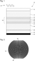
- FIG. 1 illustrates a reflective liquid crystal display device 10 of a watch according to one embodiment of the invention.
- the display device 10 includes an absorbent and transmissive front polarizer 12 (absorbent for light polarization and transmissive for orthogonal polarization), a transparent front substrate 14, a structured transparent front electrode 16, a front alignment layer 18 , a liquid crystal composition 20, a rear alignment layer 22, a structured transparent rear electrode 24, a rear substrate 26, a decorative pattern 28, a reflective and transmissive rear polarizer 30 and a black background 32 (or, according to one another embodiment, colored).
- the rear polarizer 30 can be an absorbing and transmissive polarizer associated with a reflector.
- the display device 10 is reflective in the sense that the incident surrounding light 34 is used as a light source for the display.
- the incident surrounding light 34 passes through the different layers of the display device 10 in the order listed above, is reflected on the rear polarizer 30 and returns towards the user's eye.
- the superposition of the structured electrodes 16, 24 defines a set of shape pixels that can be switched between two optical states.
- the electrodes 16, 24 are connected to a voltage source (not shown) via a control circuit (not shown).
- the application of voltage (or the absence of application) makes it possible to carry out a switching between the two optical states of the liquid crystals 20.
- the front substrate 14 and the rear substrate 26 may be made of glass or plastic.
- the substrates 14, 26 are arranged in opposite directions to create a liquid crystal cell 36 between the front substrate and the rear substrate.
- the liquid crystal cell 36 which includes the front electrode 16, the front alignment layer 18, the liquid crystal composition 20, the rear alignment layer 22 and the rear electrode 24.
- the alignment layers 18, 22 force the liquid crystals 20 to adopt a helical configuration when no electric field is applied by the electrodes 16, 24.
- the alignment layers 18, 22 can be, e.g. e.g., polyimide.
- the display device 10 can operate in “normally white” mode, that is to say a mode in which light is reflected when no electric field is applied to the liquid crystals, or in “normally black” mode, that is to say a mode in which light is not reflected when no electric field is not applied to liquid crystals.
- “normally white” mode that is to say a mode in which light is reflected when no electric field is applied to the liquid crystals
- “normally black” mode that is to say a mode in which light is not reflected when no electric field is not applied to liquid crystals.
- the other optical state is reached when an electric field is applied between the electrodes 16, 24.
- the liquid crystals 20 of the display device 10 are arranged according to several units (also called shape pixels), defined by the structured electrodes 16, 24, switchable independently in the sense that the optical state of a first pixel of shape n does not affect the optical state of a second shape pixel directly adjacent to the first shape pixel.
- the different shape pixels are switched using a voltage delivered by the structured electrodes 16, 24.
- Fig. 2 illustrates a possible structuring of the electrodes 16, 24.
- Pixels of shape 38 i in black on the Fig. 2
- in the shape of crescents are defined in order to be able to selectively switch the state of the liquid crystals located at the pixels of shape 38 i , between the front electrode 16 and the rear electrode 24.
- a pixel of switching shape 38 i covers one or more elements of the decorative layer. These elements may be continuous parts of the decorative pattern and/or pixels forming said decorative pattern in the case of a high resolution image.
- Shape pixels can be arranged regularly (e.g. for raster displays) or not. The shape of shape pixels is not limited. As indicated above, they can have, for example, a crescent shape, or more simply a rectangular or square shape when observed from above the display.
- the front substrate 14 and/or the rear substrate 26 have a thickness in the range from 50 ⁇ m to 1 mm, preferably in the range from 80 ⁇ m to 0.5 mm.
- the decorative pattern 28 is digitally printed by inkjet directly on the external surface of the rear substrate 26.
- the pattern may include absorbent zones and transparent zones allowing the light to (partially) pass through. through the decorative pattern to reach the rear polarizer 30.
- the fact of directly printing the decorative layer on the substrate 26 mitigates several disadvantages of the solutions proposed by the prior art.
- the alignment between the elements of the decorative pattern and the switching segments 38 i is more precise.
- the alignment can generally be achieved with a precision of 5 ⁇ m or less, because the decorative pattern 28 is very close to the switching segments 38 i defined by the structured electrodes 16,24 compared to the solutions of the prior art.
- This has the consequence that the switching segments 38 i cover exactly the desired areas of the decorative pattern, regardless of the viewing angle of the display device.
- the offset is less than 5 ⁇ m and will therefore not be visible to the naked eye by the user. The aesthetics will appear flawless.
- the alignment can be carried out optically with respect to the switching segments 38 i during the manufacture of the display, before other layers prevent visualization of the electrodes, in particular the structure of the electrodes.
- the parallax is reduced to the thickness of the substrate alone. The use of thin substrates (50 to 300 ⁇ m) makes it possible to reduce parallax so that the resulting optical defects are not perceptible at the naked eye.
- the decorative pattern 28 includes very small transparent openings, more light can be reflected because the decorative pattern 28 is located directly under the substrate and without a support film between the decorative layer and the rear polarizer 30. light reflected with a large angle of incidence are then less likely to be absorbed. The reflectivity (and therefore the visibility) of the decorative pattern 28 is thus improved compared to the prior art.
- the decorative pattern 28 can be applied to the external surface of the front substrate 14 instead of being applied to the external surface of the rear substrate 26 (see first embodiment). It is obviously possible to combine the first and second embodiments in order to obtain a display device comprising two decorative patterns.
- one or more photo-structurable resins can be deposited and structured by photolithography on the external surface of the front substrate 14 and/or on the external surface of the rear substrate 26.
- the resins can be colored or black and be arranged so as to form a decorative pattern 28 after deposition.
- the decorative pattern 28 can be a thin metallic layer (e.g. a layer of aluminum, a layer of gold, a layer of silver, a layer of chrome) and /or dielectric (e.g. a layer of colored oxy-nitrides) deposited by physical or chemical vapor deposition.
- the decorative pattern 28 can be structured, in particular by photolithography-engraving. It is also possible to carry out the deposition and structuring in a single step by deposition through a mask.
- the front substrate may be associated with an absorbing and transmissive front polarizer and the rear substrate may be associated with a reflector.
- the decorative pattern is disposed between the front substrate and the front polarizer.
- the liquid crystal composition may include a dichroic dye.
- the rear substrate is associated with a reflector.
- the decorative pattern can then be placed either on the external surface of the front substrate or between the rear substrate and the reflector.
- the front substrate is associated with a transmissive absorbing polarizer and the rear substrate is associated with a reflector.
- the decorative pattern can then be placed either between the front polarizer and the front substrate or between the rear substrate and the reflector.
- the rear substrate is associated with an absorbing reflective rear polarizer. The decorative pattern can then be placed between the rear polarizer and the rear substrate.
- the display device 10 can be transflective.
- the display device 10 comprises a backlight 40 arranged at the rear of a semi-transparent black background 32 (see Fig. 3 ).
- the semi-transparent black background 32 could be replaced by an absorbing/transparent polarizer.
- the rear polarizer 30 could be replaced by a reflective/transmissive polarizer partially effective in its reflective function, and the black background 32 would be replaced by an absorbing/transmissive polarizer or a semi-reflective background. -absorbent.
- the rear polarizer assembly 30 and the black background 32 would be replaced by a transflective polarizer.
- the backlight emits light 42 and may include one or more inorganic light-emitting diodes and/or one or more organic light-emitting diodes.
- the display device 10 can be transmissive.
- the display device 10 comprises a backlighting 40 arranged at the rear of a display device characterized in that the rear polarizer 30 is an absorbing/transmissive polarizer and that there is no longer a black background.
- An example of application of such a display device in watchmaking or jewelry consists of producing a moon phase by combining a high-resolution decorative pattern of the moon with a liquid crystal cell whose electrode segments are arranged to form a multitude of crescents (see Fig. 2 ) which, aligned with the decorative pattern of the moon, make it possible to display the evolution of the phases of the moon.
- the liquid crystal display device serves to hide the parts of the moon that are currently hidden by the Earth's shadow.
- the electrodes include other segments to display additional information such as time, date, day, meteorological, barometric, altimetric information or to animate decorative or playful elements such as twinkling stars in the starry sky around the Moon.
- the present invention also has an interest in sportswear type products.
- the pattern being an image of a star and the display device comprising a plurality of pixels of switchable shape defined by the transparent structured electrodes representing shaped segments capable of representing an animated image of said star in order to represent said eclipse.
- the transparent structured electrodes representing shaped segments capable of representing an animated image of said star in order to represent said eclipse.
- other celestial objects such as comets, natural satellites or not can be represented in a similar manner on the dynamic display.
- the associated backlighting device can emit a modular color to better match the reality of the colors of the object of the pattern to be represented, particularly during partial or total eclipses.
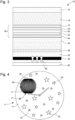
- a dial assembly 44 for a timepiece comprising a dial 46 and a display device liquid crystals 48 of the type described in connection with the figures 1 to 3 .
- the display device 48 is visible through a window 50 provided in the dial 46.
- the dial 46 includes a fixed image which forms the sky with fixed stars 52, and the decorative pattern of the display represents a moon in the form of several pixels of shape 38i as described previously in connection with the figure 2 , said pattern being able to represent the evolution of the phases of the moon in a dynamic manner.
- the decorative pattern may represent, in the form of a set of shaped pixels, certain planets, comets or other celestial objects (natural satellites or not) which will be represented by the liquid crystal display device in a dynamic manner.
Landscapes
- Physics & Mathematics (AREA)
- Nonlinear Science (AREA)
- General Physics & Mathematics (AREA)
- Optics & Photonics (AREA)
- Crystallography & Structural Chemistry (AREA)
- Chemical & Material Sciences (AREA)
- Mathematical Physics (AREA)
- Geometry (AREA)
- Liquid Crystal (AREA)
- Astronomy & Astrophysics (AREA)
- Electric Clocks (AREA)
- Devices For Indicating Variable Information By Combining Individual Elements (AREA)
- Polarising Elements (AREA)
Description
- L'invention concerne un dispositif d'affichage à cristaux liquides, un ensemble de cadran pour pièce d'horlogerie comprenant un cadran et un tel dispositif d'affichage. L'invention concerne également une pièce d'horlogerie et/ou de bijouterie comprenant un tel dispositif d'affichage ainsi qu'un procédé de fabrication d'un tel dispositif d'affichage à cristaux liquides.
- Les dispositifs d'affichage à cristaux liquides sont bien connus dans le domaine horloger depuis les années soixante-dix. À l'époque, les dispositifs d'affichage à cristaux liquides étaient utilisés pour afficher ou cacher différents segments qui formaient, ensemble, des chiffres pour p. ex. indiquer l'heure.
- Actuellement, les possibilités offertes par les affichages à cristaux liquides se sont bien développées. Par exemple, un décor imprimé sur un film plastique peut être placé entre les polariseurs de l'affichage. L'affichage peut laisser apparaitre sélectivement différentes parties du décor imprimé. Le film en plastique transparent peut recevoir un décor imprimé digitalement par jet d'encre. Les encres de l'image peuvent être opaques ou semi-transparentes pour réaliser des filtres de couleur. Le film et son impression sont laminés au moyen d'un film adhésif optiquement transparent sur la face arrière de la cellule à cristaux liquides. Il est aussi possible de laminer le film et son impression sur la face avant de la cellule à cristaux liquides. Le film adhésif a typiquement une hauteur comprise entre 15 µm et 100 µm.
- Une autre possibilité est de décorer la face avant du polariseur supérieur par une impression d'encre, le plus souvent par sérigraphie. Évidemment, il est possible de décorer la face arrière du polariseur arrière par une impression d'encre, aussi le plus souvent par sérigraphie.
- D'autre part, il existe des affichages à cristaux liquides matriciels couleurs. Ces derniers utilisent des filtres de couleur (rouge, vert, bleu et noir) pour filtrer la couleur des pixels de la matrice (rouge, vert ou bleu) ou masquer les zones entre les pixels (avec du noir). Ces filtres de couleurs sont généralement placés sur la face intérieure du substrat avant de la cellule à cristaux liquides, sous l'électrode transparente. Ces filtres sont réalisés par impression digitale ou par application de résines photostructurables qui sont structurées en bain chimique par procédé de photolithographie. Introduire les filtres dans la cellule sous l'électrode ajoute une complication technologique au procédé dans le sens, qu'après avoir réalisé ces multiples filtres de couleur, il est nécessaire d'ajouter une couche de planarisation sur laquelle est déposée l'électrode transparente. Les documents suivants sont utiles à la compréhension de l'invention:
US 2002/071069 A1 ,JP 2008 083607 A US 2004/257496 A1 etUS 2008/123473 A1 . - Un premier aspect de l'invention concerne un dispositif d'affichage à cristaux liquides (LCD), le dispositif d'affichage étant suivant la revendication 1 et comprenant entre autres: deux substrats transparents en regard désignés respectivement substrat avant et substrat arrière, le substrat avant étant celui disposé côté observateur, les substrats avant et arrière étant pourvus sur leurs faces internes d'électrodes structurées transparentes dont la superposition définit un pixel de forme commutable entre deux états optiques, les électrodes étant reliées à une source de tension par l'intermédiaire d'un circuit de commande, formant une cellule fermée par un cadre de scellement pour recevoir dans l'espace délimité par les substrats et le cadre de scellement une composition de cristaux liquides. Le dispositif comprend en plus un motif décoratif en contact direct avec le substrat avant et/ou le substrat arrière
- Il sera apprécié que le fait d'avoir un contact direct entre le motif décoratif et un des substrats permet plusieurs avantages : A) L'alignement du motif décoratif par rapport au pixel de forme commutable de l'affichage à cristaux liquides est meilleur car le décor et le pixel de forme sont plus proches. D'une part, l'alignement peut être réalisé plus facilement (p. ex. optiquement) par rapport aux pistes conductrices pendant le procédé de fabrication de la montre, avant que différents films optiques n'empêchent de visualiser précisément les pistes conductrices. B) D'autre part, la parallaxe est réduite à la seule épaisseur du substrat (p. ex. lorsque des substrats minces, de 50 à 300 µm d'épaisseur, sont utilisés, la parallaxe est très faible et les défauts optiques résultants ne sont pas perceptibles à l'oeil nu). C) Parallaxe réduite et alignement précis permettent la réalisation d'une image fine et à haut degré de détails qui s'harmonise bien avec le pixel de forme du LCD. Il n'y a ainsi pas de crosstalk et le pixel de forme peut couvrir exactement la zone souhaitée du décor, quel que soit l'angle d'observation, résultant en une image animée de haute qualité. D) Parce que la couche décorative est en contact direct avec le substrat du LCD et sans film de support, elle est au plus près du réflecteur, ce qui permet à une image de haute résolution ayant de très petites ouvertures de réfléchir plus de lumière. La réflectivité de l'image est ainsi améliorée, car les rayons lumineux réfléchis avec un angle d'incidence important sont moins susceptibles d'être absorbés.
- Les électrodes structurées transparentes peuvent être en oxyde d'indium-étain (ITO), ou en oxyde d'indium-zinc (IZO) ou tout autre électrode transparente couramment utilisée dans la fabrication d'affichages électroniques.
- Selon un mode de réalisation, la cellule à cristaux liquides peut comprendre une ou plusieurs couches d'alignement de cristaux liquides arrangées sur les électrodes. Préférablement, les une ou plusieurs couches d'alignement de cristaux liquides imposent un mode de cristaux liquides nématiques disposé en hélice (« twisted nematic » en anglais) ou un mode de cristaux liquides nématiques en super hélice (« super-twisted nematic » en anglais) aux cristaux liquides dans la cellule à cristaux liquides. D'autres modes peuvent être considérées, telles que le mode VA (pour « vertical alignement ») ou le mode ECB (pour « electrically controlled biréfringence » ou d'autres variations dérivants de la combinaison des modes précités).
- Le motif décoratif peut être disposé sur une surface externe des substrats avant ou arrière. Préférablement, le motif décoratif est disposé sur la surface externe du substrat arrière.
- Selon l'invention telle que revendiquée, le motif décoratif est aligné avec les électrodes structurées.
- Le motif décoratif peut être, non selon l'invention telle que revendiquée, une image complémentaire aux pixels de forme définis par les électrodes.
- Le motif décoratif est, selon l'invention telle que revendiquée, un motif décoratif imprimé digitalement, éventuellement par jet d'encre, ou comprendre une couche d'encre structurée. L'impression digitale fait référence à un procédé pour imprimer une image numérique sur un substrat. Les méthodes d'impression digitale selon l'invention telle que revendiquée sont l'impression à jet d'encre et l'impression laser. Dans les procédés d'impression à jet d'encre, l'image est formée par la projection de gouttelettes d'encre sur le substrat. L'encre peut comprendre des pigments et/ou des teintures en tant que colorants. L'encre peut être photosensible ou non. Le motif décoratif est préférablement imprimé digitalement par jet d'encre.
- Alternativement ou additionnellement, le motif décoratif peut comprendre une ou plusieurs couches de résines photosensibles structurées et/ou une ou plusieurs couches minces décoratives structurées (métalliques, diélectrique absorbante (p. ex : TiAION, WO, TiN...) ou miroir diélectrique).
- L'ensemble des couches formant le motif décoratif est porté directement par le substrat avant ou le substrat arrière.
- Le substrat avant et/ou substrat arrière peut avoir une épaisseur comprise dans l'intervalle allant de 50 µm à 1 mm, préférablement dans l'intervalle allant de 80 µm à 0.5 mm.
- Selon un mode de réalisation, le substrat avant est associé à un polariseur avant absorbant et transmissif. De plus, le substrat arrière est associé à un polariseur arrière réflectif et absorbant. Le motif décoratif est disposé entre le substrat arrière et le polariseur arrière.
- Selon un mode de réalisation, le substrat avant est associé à un polariseur avant absorbant et transmissif. De plus, le substrat arrière est associé à un polariseur arrière réflectif et absorbant. Le motif décoratif est disposé entre le substrat avant et le polariseur avant.
- Selon un mode de réalisation, le substrat avant est associé à un polariseur avant absorbant et transmissif. De plus, le substrat arrière est associé à un réflecteur. Le motif décoratif est disposé entre le substrat avant et le polariseur avant.
- La composition de cristaux liquides peut comprendre un colorant dichroïque. Le substrat arrière est alors associé à un réflecteur. Le motif décoratif peut être disposé soit sur la surface externe du substrat avant soit entre le substrat arrière et le réflecteur.
- Selon un mode de réalisation, la composition de cristaux liquides comprend un colorant dichroïque. Le substrat avant est associé à un polariseur absorbant transmissif. Le substrat arrière est associé à un réflecteur. Le motif décoratif peut être disposé soit entre le polariseur avant et le substrat avant, soit entre le substrat arrière et le réflecteur.
- Selon un mode de réalisation, la composition de cristaux liquides comprend un colorant dichroïque. Le substrat arrière est associé à un polariseur arrière réflectif absorbant. Le motif décoratif peut être disposé entre le polariseur arrière et le substrat arrière.
- L'affichage peut être réflectif, émissif ou transflectif. Par affichage transflectif, on entend un affichage hybride réflectif et transmissif. L'affichage est transmissif dans le sens où un rétro-éclairage est arrangé derrière le substrat arrière. L'affichage est aussi réflectif dans le sens où la lumière ambiante incidente est réfléchie par un réflecteur semi-réflectif et semi-transparent derrière le substrat arrière. Dans le cas d'un affichage transflectif, le réflecteur semi-réflectif et semi-transparent combinera la propriété de réfléchir la lumière ambiante tout en permettant de transmettre la lumière du rétro-éclairage.
- Le polariseur arrière peut être remplacé par un polariseur transflectif. Un dispositif de rétroéclairage peut être disposé à l'arrière du polariseur transflectif.
- Le polariseur arrière peut être remplacé par un polariseur absorbant transparent. Un dispositif de rétroéclairage peut être disposé à l'arrière du polariseur transflectif.
- Selon un mode de réalisation particulier de l'invention le motif décoratif est en contact direct avec le substrat avant et avec le substrat arrière et dans lequel le motif décoratif est réalisé en au moins deux portions de motif complémentaire l'une de l'autre la juxtaposition des deux portions de motif complémentaires formant ledit motif décoratif.
- Un second aspect de l'invention concerne une pièce d'horlogerie et/ou de bijouterie (p. ex une montre) et/ou une pièce d'électronique portative (p. ex. sportswear intelligent, instruments de mesure portatifs, etc...) et/ou non-portative (p. ex. domotique) comprenant un dispositif d'affichage à cristaux liquides tel décrit ci-dessus.
- Un troisième aspect de l'invention concerne un procédé de fabrication d'un dispositif d'affichage à cristaux liquides. Le procédé comprend :
- ∘ la mise à disposition d'un substrat avant et d'un substrat arrière, les substrats avant et arrière étant pourvus sur leurs faces internes d'électrodes structurées transparentes dont la superposition définit des pixels de forme commutables entre deux états optiques;
- ∘ la disposition d'un cadre de scellements sur la face interne d'un des deux substrats ;
- ∘ le scellement des deux substrats ensembles pour définir un espace délimité par les substrats ;
- ∘ le remplissage de l'espace délimité par les substrats avec une composition de cristaux liquides; et
- ∘ l'application d'un motif décoratif en contact direct avec le substrat avant ou le substrat arrière.
- L'application du motif décoratif comprend:
- ∘ soit l'impression digitale du motif décoratif, par impression laser ou par jet d'encre,
- ∘ soit l'application et la structuration, préférablement par photolithographie, d'une résine photosensible,
- ∘ soit la déposition physique ou chimique en phase vapeur d'une couche mince métallique et/ou diélectrique (typiquement inférieure à 10 microns et de préférence inférieure à 1 micron) et la structuration de la couche mince déposée, préférablement par photolithographie,
- ∘ soit une combinaison de ces méthodes d'applications.
- La combinaison de ces méthodes d'applications peut permettre l'application de plusieurs couches décoratives afin de réaliser des décors plus complexes avec différents degrés de résolution ou finesse.
- Selon encore un autre aspect l'invention concerne un ensemble de cadran pour pièce d'horlogerie comprenant un cadran et un dispositif d'affichage à cristaux liquides, le dispositif d'affichage étant selon la revendication 1 et comprenant entre autres: deux substrats transparents en regard désignés respectivement substrat avant et substrat arrière, le substrat avant étant celui disposé côté observateur, les substrats avant et arrière étant pourvus sur leurs faces internes d'électrodes structurées transparentes dont la superposition définit des pixels de forme commutables entre deux états optiques, les électrodes étant reliées à une source de tension par l'intermédiaire d'un circuit de commande, formant une cellule fermée par un cadre de scellement pour recevoir dans l'espace délimité par les substrats et le cadre de scellement une composition de cristaux liquides; et un motif décoratif en contact direct avec le substrat avant et/ou avec le substrat arrière, ledit cadran portant une image statique complémentaire à celle du motif décoratif du dispositif d'affichage. On pourra ainsi avoir, par exemple, le cadran qui forme le ciel avec étoiles fixes, et le motif décoratif pourra représenter certaines planètes, comètes ou autre objets célestes (satellites naturels ou pas) qui seront représentés par le dispositif d'affichage à cristaux liquides de manière dynamique.
- D'autres particularités et caractéristiques de l'invention ressortiront de la description détaillée de certains modes de réalisation avantageux présentés ci-dessous, à titre d'illustration, avec référence aux dessins annexés qui montrent :
- Fig. 1:
- une vue en coupe d'un dispositif d'affichage à cristaux liquide d'une montre selon un mode de réalisation de l'invention ;
- Fig. 2:
- une vue du dessus d'une électrode pour un affichage à cristaux liquide d'une montre selon un mode de réalisation de l'invention ;
- Fig. 3:
- une vue en coupe d'un dispositif d'affichage à cristaux liquide d'une montre selon un mode de réalisation de l'invention ; et
- Fig. 4:
- une vue de face d'un ensemble de cadran pour pièce d'horlogerie comprenant un cadran et un dispositif d'affichage à cristaux liquides selon l'invention.
- La
Fig. 1 illustre un dispositif d'affichage réflectif à cristaux liquides 10 d'une montre selon un mode de réalisation de l'invention. Le dispositif d'affichage 10 comprend un polariseur avant 12 absorbant et transmissif (absorbant pour une polarisation de la lumière et transmissif pour la polarisation orthogonale) , un substrat avant 14 transparent, une électrode avant 16 transparente structurée, une couche d'alignement avant 18, une composition de cristaux liquides 20, une couche d'alignement arrière 22, une électrode arrière 24 transparente structurée, un substrat arrière 26, un motif décoratif 28, un polariseur arrière 30 réflectif et transmissif et un fond noir 32 (ou, selon un autre mode de réalisation, coloré). Alternativement le polariseur arrière 30 peut être un polariseur absorbant et transmissif associé à un réflecteur. Le dispositif d'affichage 10 est réflectif dans le sens ou la lumière environnante incidente 34 est utilisée comme source de lumière pour l'affichage. La lumière environnante incidente 34 traverse les différentes couches du dispositif d'affichage 10 dans l'ordre énuméré ci-dessus, est réfléchie sur le polariseur arrière 30 et retourne vers l'oeil de l'utilisateur. La superposition des électrode 16, 24 structurées définit un ensemble de pixels de forme commutables entre deux états optiques. Les électrodes 16, 24 sont reliées à une source de tension (non représentée) par l'intermédiaire d'un circuit de commande (non représenté). L'application d'une tension (ou l'absence d'application) permet de réaliser une commutation entre les deux états optiques des cristaux liquides 20. - Le substrat avant 14 et le substrat arrière 26 peuvent être en verre ou en plastique. Les substrats 14, 26 sont arrangés de façon opposées afin de créer une cellule à cristaux liquides 36 entre le substrat avant et le substrat arrière. La cellule à cristaux liquides 36 qui comprend l'électrode avant 16, la couche d'alignement avant 18, la composition de cristaux liquides 20, la couche d'alignement arrière 22 et l'électrode arrière 24. Les couches d'alignement 18, 22 forcent les cristaux liquides 20 à adopter une configuration en hélice lorsqu'aucun champ électrique n'est appliqué par les électrodes 16, 24. Les couches d'alignement 18, 22 peuvent être, p. ex., en polyimide. Selon l'orientation des polariseurs 12, 30, le dispositif d'affichage 10 peut fonctionner en mode « normalement blanc » (« normally white » en anglais), c'est-à-dire un mode dans lequel la lumière est réfléchie lorsqu'aucun champ électrique n'est appliqué aux cristaux liquides, ou en mode « normalement noir » (« normally black » en anglais), c'est-à-dire un mode dans lequel la lumière n'est pas réfléchie lorsqu'aucun champ électrique n'est appliqué aux cristaux liquides. L'autre état optique est atteint lorsqu'un champ électrique est appliqué entre les électrodes 16, 24.
- Les cristaux liquides 20 du dispositif d'affichage 10 sont arrangés selon plusieurs unités (aussi appelés pixels de forme), définis par les électrodes structurées 16, 24, commutables indépendamment dans le sens où l'état optique d'un premier pixel de forme n'affecte pas l'état optique d'un deuxième pixel de forme directement adjacent au premier pixel de forme. Les différents pixels de forme sont commutés grâce à une tension délivrée par les électrodes 16, 24 structurées. La
Fig. 2 illustre une possible structuration des électrodes 16, 24. Des pixels de forme 38i (en noir sur laFig. 2 ) en forme de croissants sont définis afin de pouvoir sélectivement commuter l'état des cristaux liquides situés au niveau des pixels de forme 38i, entre l'électrode avant 16 et l'électrode arrière 24. Un pixel de forme de commutation 38i recouvre un ou plusieurs éléments de la couche décorative. Ces éléments peuvent être des parties continues du motif décoratif et/ou des pixels formant ledit motif décoratif dans le cas d'une image de haute résolution. Les pixels de forme peuvent être arrangés de façon régulière (p. ex. pour des affichages matriciels) ou non. La forme des pixels de forme n'est pas limitée. Comme indiqué plus haut, ils peuvent avoir p.ex. une forme de croissant, ou plus simplement une forme rectangulaire ou carrée lorsqu'ils sont observés du dessus de l'affichage. - Le substrat avant 14 et/ou le substrat arrière 26 ont une épaisseur comprise dans l'intervalle allant de 50 µm à 1 mm, préférablement dans l'intervalle allant de 80 µm à 0.5 mm. Selon un premier mode de réalisation, le motif décoratif 28 est imprimé digitalement par jet d'encre directement sur la surface externe du substrat arrière 26. Le motif peut comprendre des zones absorbantes et des zones transparentes permettant à la lumière de (partiellement) passer à travers le motif décoratif pour atteindre le polariseur arrière 30.
- Il sera apprécié que le fait d'imprimer directement la couche décorative sur le substrat 26 mitige plusieurs inconvénients des solutions proposées par l'art antérieur. En particulier, l'alignement entre les éléments du motif décoratif et les segments de commutation 38i est plus précis. L'alignement peut être généralement réalisé avec une précision de 5 µm ou moins, car le motif décoratif 28 est très proche des segments de commutation 38i définis par les électrodes structurées 16,24 par rapport aux solutions de l'art antérieur. Cela a pour conséquence que les segments de commutation 38i couvrent exactement les zones souhaitées du motif décoratif, quel que soit l'angle d'observation du dispositif d'affichage. Par « exactement », il est entendu que le décalage est de moins de 5 µm et ne sera donc pas visible à l'oeil nu par l'utilisateur. L'esthétique paraitra sans défaut. D'autre part, l'alignement peut être réalisé optiquement par rapport aux segments de commutation 38i pendant la fabrication de l'affichage, avant que d'autres couches n'empêchent de visualiser les électrodes, en particulier la structure des électrodes. Il est aussi à noter que la parallaxe est réduite à la seule épaisseur du substrat. L'utilisation de substrats minces (50 à 300 µm) permet de réduire la parallaxe de telle façon que les défauts optiques résultants ne sont pas perceptibles à l'oeil nu. De plus, même si le motif décoratif 28 comprend de très petites ouvertures transparentes, plus de lumière peut être réfléchie car le motif décoratif 28 se situe directement sous le substrat et sans film de support entre la couche décorative et le polariseur arrière 30. Les rayons lumineux réfléchis avec un angle d'incidence important sont alors moins susceptibles d'être absorbés. La réflectivité (et donc la visibilité) du motif décoratif 28 est ainsi améliorée par rapport à l'art antérieur.
- Selon un deuxième mode de réalisation de l'invention, le motif décoratif 28 peut être appliqué sur la surface externe du substrat avant 14 au lieu d'être appliqué sur la surface externe du substrat arrière 26 (voir premier mode de réalisation). Il est bien évidement possible de combiner le premier et le deuxième mode de réalisation afin d'obtenir un dispositif d'affichage comprenant deux motifs décoratifs.
- Selon un troisième mode de réalisation de l'invention, une ou plusieurs résines photo-structurables peuvent être déposées et structurées par photolithographie sur la surface externe du substrat avant 14 et/ou sur la surface externe du substrat arrière 26. Les résines peuvent être colorées ou noires et être arrangées de façon à former un motif décoratif 28 après déposition.
- Selon un quatrième mode de réalisation de l'invention, le motif décoratif 28 peut être une couche mince métallique (p. ex. une couche d'aluminium, une couche d'or, une couche d'argent, une couche de chrome) et/ou diélectrique (p. ex. une couche d'oxy-nitrures colorés) déposée par déposition physique ou chimique en phase vapeur. Le motif décoratif 28 peut être structuré, notamment par photolithographie-gravure. Il est aussi possible de réaliser la déposition et la structuration en une seule étape par déposition au travers d'un masque.
- Il est à noter qu'il est possible de combiner les motifs décoratifs 28 décrits ci-dessus afin de réaliser un motif décoratif 28 sur la surface externe du substrat avant et/ou sur la surface externe du substrat arrière comprenant un motif décoratif réalisé tel qu'indiqué ci-dessus.
- Selon d'autre modes de réalisation, d'autres arrangements de polariseurs et de motif décoratifs peuvent être contemplés. Par exemple, le substrat avant peut être associé à un polariseur avant absorbant et transmissif et le substrat arrière peut être associé à un réflecteur. Le motif décoratif est disposé entre le substrat avant et le polariseur avant.
- La composition de cristaux liquides peut comprendre un colorant dichroïque. Dans ce cas, différents arrangements peuvent aussi être contemplés. Selon un premier exemple, le substrat arrière est associé à un réflecteur. Le motif décoratif peut alors être disposé soit sur la surface externe du substrat avant soit entre le substrat arrière et le réflecteur. Selon un second exemple, le substrat avant est associé à un polariseur absorbant transmissif et le substrat arrière est associé à un réflecteur. Le motif décoratif peut alors être disposé soit entre le polariseur avant et le substrat avant soit entre le substrat arrière et le réflecteur. Selon un troisième exemple, le substrat arrière est associé à un polariseur arrière réflectif absorbant. Le motif décoratif peut alors être disposé entre le polariseur arrière et le substrat arrière.
- Selon un mode de réalisation de l'invention, le dispositif d'affichage 10 peut être transflectif. Dans ce cas, le dispositif d'affichage 10 comprend un rétroéclairage 40 arrangé à l'arrière d'un fond noir 32 semi-transparent (voir
Fig. 3 ). Dans un autre mode de réalisation, le fond noir 32 semi-transparent pourrait être remplacé par un polarisateur absorbant/transparent. Dans un autre mode de réalisation de dispositif d'affichage transflectif, le polariseur arrière 30 pourrait être remplacé par un polariseur réflectif/transmissif partiellement efficace dans sa fonction réflective, et le fond noir 32 serait remplacé par un polariseur absorbant/transmissif ou un fond semi-absorbant. Dans un autre mode, l'ensemble polariseur arrière 30 et le fond noir 32 serait remplacé par un polariseur transflectif. Le rétroéclairage émet de la lumière 42 et peut comprendre une ou plusieurs diodes électroluminescentes inorganiques et/ou une ou plusieurs diodes électroluminescentes organiques. - Selon un mode de réalisation de l'invention, le dispositif d'affichage 10 peut être transmissif. Dans ce cas, le dispositif d'affichage 10 comprend un rétroéclairage 40 arrangé à l'arrière d'un dispositif d'affichage caractérisé en ce que le polariseur arrière 30 est un polariseur absorbant/transmissif et qu'il n'y a plus de fond noir.
- Un exemple d'application d'un tel dispositif d'affichage dans l'horlogerie ou la bijouterie consiste en la réalisation d'une phase de lune par la combinaison d'un motif décoratif de haute résolution de la lune avec une cellule à cristaux liquides dont les segments des électrodes sont arrangés pour former une multitude de croissants (voir
Fig. 2 ) qui, alignés avec le motif décoratif de la lune, permettent d'afficher l'évolution des phases de la lune. Le dispositif d'affichage à cristaux liquides sert à cacher les parties de la lune qui sont actuellement cachées par l'ombre de la Terre. Il est aussi possible que les électrodes comprennent d'autres segments pour afficher des informations supplémentaires telles que l'heure, la date, le jour, des informations météorologiques, barométrique, altimétriques ou pour animer des éléments décoratifs ou ludiques tels que des étoiles scintillantes dans le ciel étoilé autour de la Lune. Il est à noter que la présente invention a aussi un intérêt dans les produits type sportswear. - On peut également envisager selon une variante de l'invention de faire de même avec une éclipse de soleil ou de lune, le motif étant une image d'un astre et le dispositif d'affichage comprenant une pluralité de pixels de forme commutables définis par les électrodes structurées transparentes et représentant des segments de forme aptes à représenter une image animée dudit astre afin de représenter ladite éclipse. Bien entendu d'autres objet celeste telles que des comètes, satellites naturels ou pas peuvent être représentés de manière analogue sur l'affichage de manière dynamique.
- On notera que lorsque dispositif est combiné avec un transflecteur à l'arrière le dispositif de rétroéclairage associé peut émettre une couleur modulable pour mieux coller à la réalité des couleurs de l'objet du motif à représenter, notamment lors d'éclipses partielles ou totales.
- A la
figure 4 est représenté un ensemble de cadran 44 pour pièce d'horlogerie (non représenté) comprenant un cadran 46 et un dispositif d'affichage à cristaux liquides 48 du type de celui décrit en liaison avec lesfigures 1 à 3 . Le dispositif d'affichage 48 est visible à travers un fenêtre 50 prévue dans le cadran 46. Dans l'exemple illustré, le cadran 46 comprend une image fixe qui forme le ciel avec étoiles fixes 52, et le motif décoratif de l'affichage représente une lune sous forme de plusieurs pixels de forme 38i comme décrit précédemment en liaison avec lafigure 2 , ledit motif pouvant représenter l'évolution des phases de la lune de manière dynamique. Alternativement, le motif décoratif pourra représenter, sous forme d'un ensemble de pixels de forme, certaines planètes, comètes ou autre objets célestes (satellites naturels ou pas) qui seront représentés par le dispositif d'affichage à cristaux liquides de manière dynamique. - Alors que des modes de réalisation particuliers viennent d'être décrits en détail, l'homme du métier appréciera que diverses modifications et alternatives à ceux-là peuvent être développées à la lumière de l'enseignement global apporté par la présente divulgation de l'invention. Par conséquent, les agencements et/ou procédés spécifiques décrits ci-dedans sont censés être donnés uniquement à titre d'illustration, sans intention de limiter la portée de l'invention, qui est déterminée par l'étendue des revendications rattachées.
Claims (19)
- Dispositif d'affichage à cristaux liquides, le dispositif d'affichage comprenant :deux substrats transparents en regard désignés respectivement substrat avant et substrat arrière, le substrat avant étant celui disposé côté observateur, les substrats avant et arrière étant pourvus sur leurs faces internes d'électrodes structurées transparentes dont la superposition définit des pixels de forme commutables entre deux états optiques, les électrodes étant reliées à une source de tension par l'intermédiaire d'un circuit de commande, formant une cellule fermée par un cadre de scellement pour recevoir dans l'espace délimité par les substrats et le cadre de scellement une composition de cristaux liquides; etun motif décoratif en contact direct avec le substrat avant et/ou avec le substrat arrière caractérisé en ce que le motif décoratif comportant des éléments alignés avec les électrodes structurées, de sorte que les pixels de forme recouvrent un ou plusieurs éléments du motif décoratif, et en ce que le motif décoratif est appliqué soit par impression digitale par jet d'encre ou impression laser, soit par l'application et la structuration, d'une résine photosensible, soit par la déposition physique ou chimique en phase vapeur d'une couche mince métallique et/ou diélectrique et la structuration de la couche mince déposée, soit par une combinaison de ces méthodes.
- Dispositif d'affichage selon la revendication 1 caractérisé en ce que le motif décoratif est disposé sur une surface externe des substrats avant ou arrière.
- Dispositif d'affichage selon la revendication 1 ou 2, caractérisé en ce que le motif décoratif est disposé sur la surface externe du substrat arrière.
- Dispositif d'affichage selon l'une quelconque des revendications précédentes caractérisé en ce que le motif décoratif comprend la combinaison d'une couche d'encre structurée, photosensibles ou non, d'une couche mince métallique, l'ensemble de ces couches décoratives étant porté directement par le substrat avant ou le substrat arrière.
- Dispositif d'affichage selon l'une quelconque des revendications 1 à 4, dans lequel le substrat avant est associé à un polariseur avant absorbant et transmissif et dans lequel le substrat arrière est associé à un polariseur arrière réflectif et absorbant, et dans lequel le motif décoratif est disposé entre le substrat arrière et le polariseur arrière.
- Dispositif d'affichage selon l'une quelconque des revendications 1 à 4, dans lequel le substrat avant est associé à un polariseur avant absorbant et transmissif et dans lequel le substrat arrière est associé à un polariseur arrière réflectif et absorbant, et dans lequel le motif décoratif est disposé entre le substrat avant et le polariseur avant.
- Dispositif d'affichage selon l'une quelconque des revendications 1 à 4, dans lequel le substrat avant est associé à un polariseur avant absorbant et transmissif et dans lequel le substrat arrière est associé à un réflecteur et dans lequel le motif décoratif est disposé entre le substrat avant et le polariseur avant.
- Dispositif d'affichage selon l'une quelconque des revendications 1 à 4, dans lequel la composition de cristaux liquides comprend un colorant dichroïque et dans lequel le substrat arrière est associé à un réflecteur et dans lequel le motif décoratif est disposé soit sur la surface externe du substrat avant soit entre le substrat arrière et le réflecteur.
- Dispositif d'affichage selon l'une quelconque des revendications 1 à 4, dans lequel la composition de cristaux liquides comprend un colorant dichroïque, dans lequel le substrat avant est associé à un polariseur absorbant transmissif et dans lequel le substrat arrière est associé à un réflecteur et dans lequel le motif décoratif est disposé soit entre le polariseur avant et le substrat avant soit entre le substrat arrière et le réflecteur.
- Dispositif d'affichage selon l'une quelconque des revendications 1 à 4, dans lequel la composition de cristaux liquides comprend un colorant dichroïque, dans lequel le substrat arrière est associé à un polariseur arrière réflectif absorbant et dans lequel le motif décoratif est disposé entre le polariseur arrière et le substrat arrière.
- Dispositif d'affichage selon l'une quelconque des revendications 5, 6 ou 10, dans lequel le polariseur arrière est remplacé par un polariseur transflectif et dans lequel un dispositif de rétroéclairage est disposé à l'arrière du polariseur transflectif.
- Dispositif d'affichage selon l'une quelconque des revendications 5, 6 ou 10, dans lequel le polariseur arrière est remplacé par un polariseur absorbant transmissif et dans lequel un dispositif de rétroéclairage est disposé à l'arrière du polariseur transflectif.
- Dispositif d'affichage selon la revendication 11 ou 12 dans lequel le dispositif de rétroéclairage émet une lumière dont la couleur est modulable.
- Dispositif d'affichage selon l'une quelconque des revendications dans lequel le motif décoratif est en contact direct avec le substrat avant et avec le substrat arrière et dans lequel le motif décoratif est réalisé en au moins deux portions de motif complémentaire l'une de l'autre la juxtaposition des deux portions de motif complémentaires formant ledit motif décoratif.
- Ensemble de cadran pour pièce d'horlogerie comprenant un cadran et un dispositif d'affichage selon l'une quelconque des revendications 1 à 14, ledit cadran portant une image statique complémentaire à celle du motif décoratif du dispositif d'affichage.
- Pièce d'horlogerie et/ou de bijouterie comprenant un dispositif d'affichage selon l'une quelconque des revendications 1 à 14.
- Pièce d'horlogerie et/ou de bijouterie selon la revendication 16, caractérisée en ce que le motif est une image d'un astre, le dispositif d'affichage comprenant une pluralité de pixels de forme commutables définis par les électrodes structurées transparentes et représentant des segments de forme aptes à représenter une image animée dudit astre.
- Pièce d'horlogerie et/ou de bijouterie selon la revendication 17, caractérisé en ce que l'astre est la lune et en ce que la pluralité de pixels de forme commutables définis par les électrodes structurées transparentes et représentent des segments en forme de croissants représentant les phases de lune.
- Un procédé de fabrication d'un dispositif d'affichage à cristaux liquides selon l'une quelconque des revendications 1 à 18, le procédé comprenant :la mise à disposition d'un substrat avant et un substrat arrière, les substrats avant et arrière étant pourvus sur leurs faces internes d'électrodes structurées transparentes dont la superposition définit des pixels de forme commutables entre deux états optiques;la disposition d'un cadre de scellements sur la face interne d'un des deux substrats ;le scellement des deux substrats ensembles pour définir un espace délimité par les substrats ;le remplissage de l'espace délimité par les substrats avec une composition de cristaux liquides; etl'application d'un motif décoratif en contact direct avec le substrat avant ou le substrat arrière et dans lequel l'application du motif décoratif comprend :∘ soit l'impression digitale du motif décoratif par jet d'encre ou par impression laser,∘ soit l'application et la structuration, préférablement par photolithographie, d'une résine photosensible,∘ soit la déposition physique ou chimique en phase vapeur d'une couche mince métallique et/ou diélectrique et la structuration de la couche déposée, préférablement par photolithographie,∘ soit une combinaison de ces méthodes d'applications.
Priority Applications (6)
| Application Number | Priority Date | Filing Date | Title |
|---|---|---|---|
| EP19217221.1A EP3839617B1 (fr) | 2019-12-17 | 2019-12-17 | Dispositif d affichage à cristaux liquides |
| US17/000,600 US12007633B2 (en) | 2019-12-17 | 2020-08-24 | Liquid crystal display device with decorative pattern directly thereon |
| JP2020151791A JP2021096222A (ja) | 2019-12-17 | 2020-09-10 | 液晶ディスプレイ・デバイス |
| CN202011491337.9A CN112987365A (zh) | 2019-12-17 | 2020-12-17 | 液晶显示装置 |
| JP2022152746A JP7334318B2 (ja) | 2019-12-17 | 2022-09-26 | 液晶ディスプレイ・デバイス |
| US18/480,718 US12140829B2 (en) | 2019-12-17 | 2023-10-04 | Liquid crystal display device with decorative pattern directly aligned with transparent structured electrodes |
Applications Claiming Priority (1)
| Application Number | Priority Date | Filing Date | Title |
|---|---|---|---|
| EP19217221.1A EP3839617B1 (fr) | 2019-12-17 | 2019-12-17 | Dispositif d affichage à cristaux liquides |
Publications (2)
| Publication Number | Publication Date |
|---|---|
| EP3839617A1 EP3839617A1 (fr) | 2021-06-23 |
| EP3839617B1 true EP3839617B1 (fr) | 2024-06-26 |
Family
ID=68944356
Family Applications (1)
| Application Number | Title | Priority Date | Filing Date |
|---|---|---|---|
| EP19217221.1A Active EP3839617B1 (fr) | 2019-12-17 | 2019-12-17 | Dispositif d affichage à cristaux liquides |
Country Status (4)
| Country | Link |
|---|---|
| US (2) | US12007633B2 (fr) |
| EP (1) | EP3839617B1 (fr) |
| JP (2) | JP2021096222A (fr) |
| CN (1) | CN112987365A (fr) |
Families Citing this family (4)
| Publication number | Priority date | Publication date | Assignee | Title |
|---|---|---|---|---|
| JP2022129506A (ja) * | 2021-02-25 | 2022-09-06 | 日東電工株式会社 | 加飾フィルム |
| CN119148432A (zh) * | 2023-06-15 | 2024-12-17 | 群创光电股份有限公司 | 电子装置 |
| CN119225065A (zh) * | 2023-06-23 | 2024-12-31 | 上海天马微电子有限公司 | 显示装置 |
| CN118033942B (zh) * | 2024-02-22 | 2025-12-30 | 惠科股份有限公司 | 一种显示面板、显示装置和显示系统 |
Citations (4)
| Publication number | Priority date | Publication date | Assignee | Title |
|---|---|---|---|---|
| US20020071069A1 (en) * | 1997-08-01 | 2002-06-13 | Koji Nakagawa | Light scattering type liquid crystal display panel for timepiece |
| US20040257496A1 (en) * | 2003-06-20 | 2004-12-23 | Casio Computer Co., Ltd. | Display device and manufacturing method of the same |
| JP2008083607A (ja) * | 2006-09-29 | 2008-04-10 | Casio Comput Co Ltd | 液晶表示装置およびその製造方法 |
| US20080123473A1 (en) * | 2005-08-10 | 2008-05-29 | Seiko Epson Corporation | Electronic component and electronic device |
Family Cites Families (20)
| Publication number | Priority date | Publication date | Assignee | Title |
|---|---|---|---|---|
| JPS5560921A (en) | 1978-11-01 | 1980-05-08 | Toshiba Corp | Liquid crystal display element |
| US5245590A (en) * | 1992-07-10 | 1993-09-14 | Galison William A | Display of changing moon on watch face |
| FR2743924B1 (fr) * | 1996-01-23 | 1998-05-22 | Asulab Sa | Dispositif d'affichage d'un decor et piece d'horlogerie le comprenant |
| JP3702643B2 (ja) | 1997-06-09 | 2005-10-05 | セイコーエプソン株式会社 | 表示装置及び電子時計 |
| EP0939331B1 (fr) * | 1998-02-27 | 2010-04-14 | Asulab S.A. | Ensemble d'affichage comprenant deux dispositifs d'affichage superposés |
| JP2000221282A (ja) * | 1999-01-29 | 2000-08-11 | Citizen Watch Co Ltd | 時 計 |
| US20050030836A1 (en) * | 2003-04-04 | 2005-02-10 | Tom Burns | Watch with mirror dial plate |
| JP2004329692A (ja) * | 2003-05-09 | 2004-11-25 | Hitachi Displays Ltd | 表示装置および遊技機 |
| JP2007047030A (ja) | 2005-08-10 | 2007-02-22 | Seiko Epson Corp | 計時装置及び計時装置用文字板 |
| US20070153162A1 (en) * | 2005-12-30 | 2007-07-05 | Wright Robin E | Reinforced reflective polarizer films |
| JPWO2007105700A1 (ja) * | 2006-03-15 | 2009-07-30 | シャープ株式会社 | アクティブマトリクス基板およびそれを用いた表示装置 |
| JP2009008710A (ja) | 2007-06-26 | 2009-01-15 | Citizen Holdings Co Ltd | 液晶表示装置 |
| JP4900206B2 (ja) * | 2007-11-26 | 2012-03-21 | パナソニック株式会社 | タッチパネル |
| US8760415B2 (en) * | 2009-03-30 | 2014-06-24 | Kent Displays Incorporated | Display with overlayed electronic skin |
| CN202230680U (zh) | 2011-09-20 | 2012-05-23 | 吴重九 | 叠合式投影显示装置 |
| US9320140B2 (en) * | 2011-12-22 | 2016-04-19 | Nissha Printing Co., Ltd. | Touch sensor with ornament, method of manufacturing same, and transparent conductive sensor used in same |
| US20140098332A1 (en) * | 2012-10-10 | 2014-04-10 | Apple Inc. | Displays With Logos and Alignment Marks |
| US9297675B2 (en) * | 2013-10-04 | 2016-03-29 | Tactotek Oy | Illuminated indicator structures for electronic devices |
| KR102018022B1 (ko) * | 2014-09-05 | 2019-09-03 | 가부시키가이샤 덴소 | 표시 장치 |
| US20180267345A1 (en) * | 2017-03-15 | 2018-09-20 | HKC Corporation Limited | Display device and display panel thereof |
-
2019
- 2019-12-17 EP EP19217221.1A patent/EP3839617B1/fr active Active
-
2020
- 2020-08-24 US US17/000,600 patent/US12007633B2/en active Active
- 2020-09-10 JP JP2020151791A patent/JP2021096222A/ja active Pending
- 2020-12-17 CN CN202011491337.9A patent/CN112987365A/zh active Pending
-
2022
- 2022-09-26 JP JP2022152746A patent/JP7334318B2/ja active Active
-
2023
- 2023-10-04 US US18/480,718 patent/US12140829B2/en active Active
Patent Citations (4)
| Publication number | Priority date | Publication date | Assignee | Title |
|---|---|---|---|---|
| US20020071069A1 (en) * | 1997-08-01 | 2002-06-13 | Koji Nakagawa | Light scattering type liquid crystal display panel for timepiece |
| US20040257496A1 (en) * | 2003-06-20 | 2004-12-23 | Casio Computer Co., Ltd. | Display device and manufacturing method of the same |
| US20080123473A1 (en) * | 2005-08-10 | 2008-05-29 | Seiko Epson Corporation | Electronic component and electronic device |
| JP2008083607A (ja) * | 2006-09-29 | 2008-04-10 | Casio Comput Co Ltd | 液晶表示装置およびその製造方法 |
Also Published As
| Publication number | Publication date |
|---|---|
| JP2021096222A (ja) | 2021-06-24 |
| US20210181564A1 (en) | 2021-06-17 |
| CN112987365A (zh) | 2021-06-18 |
| JP2022188135A (ja) | 2022-12-20 |
| EP3839617A1 (fr) | 2021-06-23 |
| JP7334318B2 (ja) | 2023-08-28 |
| US12007633B2 (en) | 2024-06-11 |
| US20240027807A1 (en) | 2024-01-25 |
| US12140829B2 (en) | 2024-11-12 |
Similar Documents
| Publication | Publication Date | Title |
|---|---|---|
| EP3839617B1 (fr) | Dispositif d affichage à cristaux liquides | |
| EP0786685B1 (fr) | Dispositif d'affichage d'un décor et pièce d'horlogerie le comprenant | |
| EP1128240B1 (fr) | Ensemble d'affichage à inversion de constrate comprenant deux dispositifs d'affichage superposés | |
| EP1040391B1 (fr) | Ensemble d'affichage comprenant deux dispositifs d'affichage superposes | |
| EP0078237B1 (fr) | Montre à dispositif d'affichage analogique dont le cadran est formé par une cellule d'affichage à cristal liquide | |
| EP3069199B1 (fr) | Cadran nacré pour afficheur caché | |
| EP3650957B1 (fr) | Objet muni d'un dispositif d'affichage électrooptique | |
| WO2007096358A1 (fr) | Dispositif d'affichage à cristaux liquides affichant des segments colorés et pièce d'horlogerie équipée de ce dispositif | |
| CH716960A2 (fr) | Dispositif d'affichage à cristaux liquides. | |
| EP0939331B1 (fr) | Ensemble d'affichage comprenant deux dispositifs d'affichage superposés | |
| HK40055763A (en) | Liquid crystal display device | |
| EP1174756B1 (fr) | Ensemble d'affichage comportant une cellule électro-optique et une cellule photovoltaique | |
| EP3128359A1 (fr) | Dispositif d'affichage pour un objet portable tel qu'une pièce d'horlogerie | |
| EP4016173B1 (fr) | Procédé de fabrication d'un dispositif d'affichage à cristal liquide et dispositif d'affichage a cristal liquide | |
| EP1085364B1 (fr) | Ensemble d'affichage comprenant deux dispositifs d'affichage superposés | |
| EP1156360B1 (fr) | Ensemble d'affichage à inversion chromatique de contraste | |
| EP1202109A1 (fr) | Dispositif d'affichage à cristaux liquides à coefficient de réflexion de la lumière élevé | |
| EP1209512A1 (fr) | Dispositif d'affichage réflectif à cristaux liquides présentant un contraste d'affichage amélioré | |
| EP4692960A1 (fr) | Dispositif à cristaux liquides pour une pièce d'horlogerie | |
| FR3021800A1 (fr) | Dispositif d'affichage reflectif a tres haute luminosite et a surface photovoltaique integree | |
| CH708838A2 (fr) | Cadran translucide ou semi-transparent pour afficheur caché. | |
| CH711421A2 (fr) | Dispositif d'affichage pour un objet portable tel qu'une pièce d'horlogerie comprenant un réseau lenticulaire. | |
| CH704113B1 (fr) | Dispositif d'affichage à cristaux liquides affichant des segments colorés et pièce d'horlogerie équipée de ce dispositif. |
Legal Events
| Date | Code | Title | Description |
|---|---|---|---|
| PUAI | Public reference made under article 153(3) epc to a published international application that has entered the european phase |
Free format text: ORIGINAL CODE: 0009012 |
|
| STAA | Information on the status of an ep patent application or granted ep patent |
Free format text: STATUS: THE APPLICATION HAS BEEN PUBLISHED |
|
| AK | Designated contracting states |
Kind code of ref document: A1 Designated state(s): AL AT BE BG CH CY CZ DE DK EE ES FI FR GB GR HR HU IE IS IT LI LT LU LV MC MK MT NL NO PL PT RO RS SE SI SK SM TR |
|
| STAA | Information on the status of an ep patent application or granted ep patent |
Free format text: STATUS: REQUEST FOR EXAMINATION WAS MADE |
|
| 17P | Request for examination filed |
Effective date: 20211223 |
|
| RBV | Designated contracting states (corrected) |
Designated state(s): AL AT BE BG CH CY CZ DE DK EE ES FI FR GB GR HR HU IE IS IT LI LT LU LV MC MK MT NL NO PL PT RO RS SE SI SK SM TR |
|
| STAA | Information on the status of an ep patent application or granted ep patent |
Free format text: STATUS: EXAMINATION IS IN PROGRESS |
|
| 17Q | First examination report despatched |
Effective date: 20230209 |
|
| P01 | Opt-out of the competence of the unified patent court (upc) registered |
Effective date: 20230615 |
|
| GRAP | Despatch of communication of intention to grant a patent |
Free format text: ORIGINAL CODE: EPIDOSNIGR1 |
|
| STAA | Information on the status of an ep patent application or granted ep patent |
Free format text: STATUS: GRANT OF PATENT IS INTENDED |
|
| INTG | Intention to grant announced |
Effective date: 20240402 |
|
| GRAS | Grant fee paid |
Free format text: ORIGINAL CODE: EPIDOSNIGR3 |
|
| GRAA | (expected) grant |
Free format text: ORIGINAL CODE: 0009210 |
|
| STAA | Information on the status of an ep patent application or granted ep patent |
Free format text: STATUS: THE PATENT HAS BEEN GRANTED |
|
| AK | Designated contracting states |
Kind code of ref document: B1 Designated state(s): AL AT BE BG CH CY CZ DE DK EE ES FI FR GB GR HR HU IE IS IT LI LT LU LV MC MK MT NL NO PL PT RO RS SE SI SK SM TR |
|
| REG | Reference to a national code |
Ref country code: GB Ref legal event code: FG4D Free format text: NOT ENGLISH |
|
| REG | Reference to a national code |
Ref country code: CH Ref legal event code: EP |
|
| REG | Reference to a national code |
Ref country code: DE Ref legal event code: R096 Ref document number: 602019054129 Country of ref document: DE |
|
| PG25 | Lapsed in a contracting state [announced via postgrant information from national office to epo] |
Ref country code: BG Free format text: LAPSE BECAUSE OF FAILURE TO SUBMIT A TRANSLATION OF THE DESCRIPTION OR TO PAY THE FEE WITHIN THE PRESCRIBED TIME-LIMIT Effective date: 20240626 |
|
| PG25 | Lapsed in a contracting state [announced via postgrant information from national office to epo] |
Ref country code: HR Free format text: LAPSE BECAUSE OF FAILURE TO SUBMIT A TRANSLATION OF THE DESCRIPTION OR TO PAY THE FEE WITHIN THE PRESCRIBED TIME-LIMIT Effective date: 20240626 Ref country code: FI Free format text: LAPSE BECAUSE OF FAILURE TO SUBMIT A TRANSLATION OF THE DESCRIPTION OR TO PAY THE FEE WITHIN THE PRESCRIBED TIME-LIMIT Effective date: 20240626 |
|
| REG | Reference to a national code |
Ref country code: LT Ref legal event code: MG9D |
|
| PG25 | Lapsed in a contracting state [announced via postgrant information from national office to epo] |
Ref country code: GR Free format text: LAPSE BECAUSE OF FAILURE TO SUBMIT A TRANSLATION OF THE DESCRIPTION OR TO PAY THE FEE WITHIN THE PRESCRIBED TIME-LIMIT Effective date: 20240927 |
|
| PG25 | Lapsed in a contracting state [announced via postgrant information from national office to epo] |
Ref country code: LV Free format text: LAPSE BECAUSE OF FAILURE TO SUBMIT A TRANSLATION OF THE DESCRIPTION OR TO PAY THE FEE WITHIN THE PRESCRIBED TIME-LIMIT Effective date: 20240626 |
|
| REG | Reference to a national code |
Ref country code: NL Ref legal event code: MP Effective date: 20240626 |
|
| PG25 | Lapsed in a contracting state [announced via postgrant information from national office to epo] |
Ref country code: NO Free format text: LAPSE BECAUSE OF FAILURE TO SUBMIT A TRANSLATION OF THE DESCRIPTION OR TO PAY THE FEE WITHIN THE PRESCRIBED TIME-LIMIT Effective date: 20240926 Ref country code: LV Free format text: LAPSE BECAUSE OF FAILURE TO SUBMIT A TRANSLATION OF THE DESCRIPTION OR TO PAY THE FEE WITHIN THE PRESCRIBED TIME-LIMIT Effective date: 20240626 Ref country code: HR Free format text: LAPSE BECAUSE OF FAILURE TO SUBMIT A TRANSLATION OF THE DESCRIPTION OR TO PAY THE FEE WITHIN THE PRESCRIBED TIME-LIMIT Effective date: 20240626 Ref country code: GR Free format text: LAPSE BECAUSE OF FAILURE TO SUBMIT A TRANSLATION OF THE DESCRIPTION OR TO PAY THE FEE WITHIN THE PRESCRIBED TIME-LIMIT Effective date: 20240927 Ref country code: FI Free format text: LAPSE BECAUSE OF FAILURE TO SUBMIT A TRANSLATION OF THE DESCRIPTION OR TO PAY THE FEE WITHIN THE PRESCRIBED TIME-LIMIT Effective date: 20240626 Ref country code: BG Free format text: LAPSE BECAUSE OF FAILURE TO SUBMIT A TRANSLATION OF THE DESCRIPTION OR TO PAY THE FEE WITHIN THE PRESCRIBED TIME-LIMIT Effective date: 20240626 Ref country code: RS Free format text: LAPSE BECAUSE OF FAILURE TO SUBMIT A TRANSLATION OF THE DESCRIPTION OR TO PAY THE FEE WITHIN THE PRESCRIBED TIME-LIMIT Effective date: 20240926 |
|
| PG25 | Lapsed in a contracting state [announced via postgrant information from national office to epo] |
Ref country code: NL Free format text: LAPSE BECAUSE OF FAILURE TO SUBMIT A TRANSLATION OF THE DESCRIPTION OR TO PAY THE FEE WITHIN THE PRESCRIBED TIME-LIMIT Effective date: 20240626 |
|
| REG | Reference to a national code |
Ref country code: AT Ref legal event code: MK05 Ref document number: 1698190 Country of ref document: AT Kind code of ref document: T Effective date: 20240626 |
|
| PG25 | Lapsed in a contracting state [announced via postgrant information from national office to epo] |
Ref country code: NL Free format text: LAPSE BECAUSE OF FAILURE TO SUBMIT A TRANSLATION OF THE DESCRIPTION OR TO PAY THE FEE WITHIN THE PRESCRIBED TIME-LIMIT Effective date: 20240626 |
|
| PG25 | Lapsed in a contracting state [announced via postgrant information from national office to epo] |
Ref country code: PT Free format text: LAPSE BECAUSE OF FAILURE TO SUBMIT A TRANSLATION OF THE DESCRIPTION OR TO PAY THE FEE WITHIN THE PRESCRIBED TIME-LIMIT Effective date: 20241028 |
|
| PG25 | Lapsed in a contracting state [announced via postgrant information from national office to epo] |
Ref country code: PT Free format text: LAPSE BECAUSE OF FAILURE TO SUBMIT A TRANSLATION OF THE DESCRIPTION OR TO PAY THE FEE WITHIN THE PRESCRIBED TIME-LIMIT Effective date: 20241028 |
|
| PG25 | Lapsed in a contracting state [announced via postgrant information from national office to epo] |
Ref country code: PL Free format text: LAPSE BECAUSE OF FAILURE TO SUBMIT A TRANSLATION OF THE DESCRIPTION OR TO PAY THE FEE WITHIN THE PRESCRIBED TIME-LIMIT Effective date: 20240626 |
|
| PG25 | Lapsed in a contracting state [announced via postgrant information from national office to epo] |
Ref country code: EE Free format text: LAPSE BECAUSE OF FAILURE TO SUBMIT A TRANSLATION OF THE DESCRIPTION OR TO PAY THE FEE WITHIN THE PRESCRIBED TIME-LIMIT Effective date: 20240626 |
|
| PG25 | Lapsed in a contracting state [announced via postgrant information from national office to epo] |
Ref country code: IS Free format text: LAPSE BECAUSE OF FAILURE TO SUBMIT A TRANSLATION OF THE DESCRIPTION OR TO PAY THE FEE WITHIN THE PRESCRIBED TIME-LIMIT Effective date: 20241026 Ref country code: AT Free format text: LAPSE BECAUSE OF FAILURE TO SUBMIT A TRANSLATION OF THE DESCRIPTION OR TO PAY THE FEE WITHIN THE PRESCRIBED TIME-LIMIT Effective date: 20240626 |
|
| PG25 | Lapsed in a contracting state [announced via postgrant information from national office to epo] |
Ref country code: CZ Free format text: LAPSE BECAUSE OF FAILURE TO SUBMIT A TRANSLATION OF THE DESCRIPTION OR TO PAY THE FEE WITHIN THE PRESCRIBED TIME-LIMIT Effective date: 20240626 |
|
| PG25 | Lapsed in a contracting state [announced via postgrant information from national office to epo] |
Ref country code: SK Free format text: LAPSE BECAUSE OF FAILURE TO SUBMIT A TRANSLATION OF THE DESCRIPTION OR TO PAY THE FEE WITHIN THE PRESCRIBED TIME-LIMIT Effective date: 20240626 Ref country code: RO Free format text: LAPSE BECAUSE OF FAILURE TO SUBMIT A TRANSLATION OF THE DESCRIPTION OR TO PAY THE FEE WITHIN THE PRESCRIBED TIME-LIMIT Effective date: 20240626 |
|
| PG25 | Lapsed in a contracting state [announced via postgrant information from national office to epo] |
Ref country code: ES Free format text: LAPSE BECAUSE OF FAILURE TO SUBMIT A TRANSLATION OF THE DESCRIPTION OR TO PAY THE FEE WITHIN THE PRESCRIBED TIME-LIMIT Effective date: 20240626 Ref country code: SM Free format text: LAPSE BECAUSE OF FAILURE TO SUBMIT A TRANSLATION OF THE DESCRIPTION OR TO PAY THE FEE WITHIN THE PRESCRIBED TIME-LIMIT Effective date: 20240626 |
|
| PG25 | Lapsed in a contracting state [announced via postgrant information from national office to epo] |
Ref country code: SM Free format text: LAPSE BECAUSE OF FAILURE TO SUBMIT A TRANSLATION OF THE DESCRIPTION OR TO PAY THE FEE WITHIN THE PRESCRIBED TIME-LIMIT Effective date: 20240626 Ref country code: SK Free format text: LAPSE BECAUSE OF FAILURE TO SUBMIT A TRANSLATION OF THE DESCRIPTION OR TO PAY THE FEE WITHIN THE PRESCRIBED TIME-LIMIT Effective date: 20240626 Ref country code: RO Free format text: LAPSE BECAUSE OF FAILURE TO SUBMIT A TRANSLATION OF THE DESCRIPTION OR TO PAY THE FEE WITHIN THE PRESCRIBED TIME-LIMIT Effective date: 20240626 Ref country code: PL Free format text: LAPSE BECAUSE OF FAILURE TO SUBMIT A TRANSLATION OF THE DESCRIPTION OR TO PAY THE FEE WITHIN THE PRESCRIBED TIME-LIMIT Effective date: 20240626 Ref country code: IS Free format text: LAPSE BECAUSE OF FAILURE TO SUBMIT A TRANSLATION OF THE DESCRIPTION OR TO PAY THE FEE WITHIN THE PRESCRIBED TIME-LIMIT Effective date: 20241026 Ref country code: ES Free format text: LAPSE BECAUSE OF FAILURE TO SUBMIT A TRANSLATION OF THE DESCRIPTION OR TO PAY THE FEE WITHIN THE PRESCRIBED TIME-LIMIT Effective date: 20240626 Ref country code: EE Free format text: LAPSE BECAUSE OF FAILURE TO SUBMIT A TRANSLATION OF THE DESCRIPTION OR TO PAY THE FEE WITHIN THE PRESCRIBED TIME-LIMIT Effective date: 20240626 Ref country code: CZ Free format text: LAPSE BECAUSE OF FAILURE TO SUBMIT A TRANSLATION OF THE DESCRIPTION OR TO PAY THE FEE WITHIN THE PRESCRIBED TIME-LIMIT Effective date: 20240626 Ref country code: AT Free format text: LAPSE BECAUSE OF FAILURE TO SUBMIT A TRANSLATION OF THE DESCRIPTION OR TO PAY THE FEE WITHIN THE PRESCRIBED TIME-LIMIT Effective date: 20240626 |
|
| PG25 | Lapsed in a contracting state [announced via postgrant information from national office to epo] |
Ref country code: IT Free format text: LAPSE BECAUSE OF FAILURE TO SUBMIT A TRANSLATION OF THE DESCRIPTION OR TO PAY THE FEE WITHIN THE PRESCRIBED TIME-LIMIT Effective date: 20240626 |
|
| REG | Reference to a national code |
Ref country code: DE Ref legal event code: R097 Ref document number: 602019054129 Country of ref document: DE |
|
| PG25 | Lapsed in a contracting state [announced via postgrant information from national office to epo] |
Ref country code: DK Free format text: LAPSE BECAUSE OF FAILURE TO SUBMIT A TRANSLATION OF THE DESCRIPTION OR TO PAY THE FEE WITHIN THE PRESCRIBED TIME-LIMIT Effective date: 20240626 |
|
| PGFP | Annual fee paid to national office [announced via postgrant information from national office to epo] |
Ref country code: CH Payment date: 20250101 Year of fee payment: 6 |
|
| PLBE | No opposition filed within time limit |
Free format text: ORIGINAL CODE: 0009261 |
|
| STAA | Information on the status of an ep patent application or granted ep patent |
Free format text: STATUS: NO OPPOSITION FILED WITHIN TIME LIMIT |
|
| 26N | No opposition filed |
Effective date: 20250327 |
|
| PG25 | Lapsed in a contracting state [announced via postgrant information from national office to epo] |
Ref country code: MC Free format text: LAPSE BECAUSE OF FAILURE TO SUBMIT A TRANSLATION OF THE DESCRIPTION OR TO PAY THE FEE WITHIN THE PRESCRIBED TIME-LIMIT Effective date: 20240626 |
|
| PG25 | Lapsed in a contracting state [announced via postgrant information from national office to epo] |
Ref country code: LU Free format text: LAPSE BECAUSE OF NON-PAYMENT OF DUE FEES Effective date: 20241217 |
|
| GBPC | Gb: european patent ceased through non-payment of renewal fee |
Effective date: 20241217 |
|
| PG25 | Lapsed in a contracting state [announced via postgrant information from national office to epo] |
Ref country code: SE Free format text: LAPSE BECAUSE OF FAILURE TO SUBMIT A TRANSLATION OF THE DESCRIPTION OR TO PAY THE FEE WITHIN THE PRESCRIBED TIME-LIMIT Effective date: 20240626 |
|
| REG | Reference to a national code |
Ref country code: BE Ref legal event code: MM Effective date: 20241231 |
|
| PG25 | Lapsed in a contracting state [announced via postgrant information from national office to epo] |
Ref country code: GB Free format text: LAPSE BECAUSE OF NON-PAYMENT OF DUE FEES Effective date: 20241217 Ref country code: BE Free format text: LAPSE BECAUSE OF NON-PAYMENT OF DUE FEES Effective date: 20241231 |
|
| PG25 | Lapsed in a contracting state [announced via postgrant information from national office to epo] |
Ref country code: IE Free format text: LAPSE BECAUSE OF NON-PAYMENT OF DUE FEES Effective date: 20241217 |
|
| REG | Reference to a national code |
Ref country code: CH Ref legal event code: U11 Free format text: ST27 STATUS EVENT CODE: U-0-0-U10-U11 (AS PROVIDED BY THE NATIONAL OFFICE) Effective date: 20260101 |
|
| PGFP | Annual fee paid to national office [announced via postgrant information from national office to epo] |
Ref country code: DE Payment date: 20251126 Year of fee payment: 7 |
|
| PGFP | Annual fee paid to national office [announced via postgrant information from national office to epo] |
Ref country code: FR Payment date: 20251120 Year of fee payment: 7 |