EP3840318B1 - I/q-abwärtsumsetzung mit spiegelfrequenzkompensation - Google Patents
I/q-abwärtsumsetzung mit spiegelfrequenzkompensation Download PDFInfo
- Publication number
- EP3840318B1 EP3840318B1 EP20213682.6A EP20213682A EP3840318B1 EP 3840318 B1 EP3840318 B1 EP 3840318B1 EP 20213682 A EP20213682 A EP 20213682A EP 3840318 B1 EP3840318 B1 EP 3840318B1
- Authority
- EP
- European Patent Office
- Prior art keywords
- signal
- processing
- input
- adaptive
- node
- Prior art date
- Legal status (The legal status is an assumption and is not a legal conclusion. Google has not performed a legal analysis and makes no representation as to the accuracy of the status listed.)
- Active
Links
Images






Classifications
-
- H—ELECTRICITY
- H03—ELECTRONIC CIRCUITRY
- H03H—IMPEDANCE NETWORKS, e.g. RESONANT CIRCUITS; RESONATORS
- H03H17/00—Networks using digital techniques
-
- H—ELECTRICITY
- H04—ELECTRIC COMMUNICATION TECHNIQUE
- H04L—TRANSMISSION OF DIGITAL INFORMATION, e.g. TELEGRAPHIC COMMUNICATION
- H04L27/00—Modulated-carrier systems
- H04L27/32—Carrier systems characterised by combinations of two or more of the types covered by groups H04L27/02, H04L27/10, H04L27/18 or H04L27/26
- H04L27/34—Amplitude- and phase-modulated carrier systems, e.g. quadrature-amplitude modulated carrier systems
- H04L27/36—Modulator circuits; Transmitter circuits
- H04L27/362—Modulation using more than one carrier, e.g. with quadrature carriers, separately amplitude modulated
- H04L27/364—Arrangements for overcoming imperfections in the modulator, e.g. quadrature error or unbalanced I and Q levels
-
- H—ELECTRICITY
- H04—ELECTRIC COMMUNICATION TECHNIQUE
- H04L—TRANSMISSION OF DIGITAL INFORMATION, e.g. TELEGRAPHIC COMMUNICATION
- H04L27/00—Modulated-carrier systems
- H04L27/32—Carrier systems characterised by combinations of two or more of the types covered by groups H04L27/02, H04L27/10, H04L27/18 or H04L27/26
- H04L27/34—Amplitude- and phase-modulated carrier systems, e.g. quadrature-amplitude modulated carrier systems
- H04L27/38—Demodulator circuits; Receiver circuits
- H04L27/3845—Demodulator circuits; Receiver circuits using non - coherent demodulation, i.e. not using a phase synchronous carrier
- H04L27/3854—Demodulator circuits; Receiver circuits using non - coherent demodulation, i.e. not using a phase synchronous carrier using a non - coherent carrier, including systems with baseband correction for phase or frequency offset
- H04L27/3863—Compensation for quadrature error in the received signal
-
- H—ELECTRICITY
- H03—ELECTRONIC CIRCUITRY
- H03F—AMPLIFIERS
- H03F1/00—Details of amplifiers with only discharge tubes, only semiconductor devices or only unspecified devices as amplifying elements
- H03F1/26—Modifications of amplifiers to reduce influence of noise generated by amplifying elements
-
- H—ELECTRICITY
- H03—ELECTRONIC CIRCUITRY
- H03H—IMPEDANCE NETWORKS, e.g. RESONANT CIRCUITS; RESONATORS
- H03H17/00—Networks using digital techniques
- H03H17/02—Frequency selective networks
-
- H—ELECTRICITY
- H03—ELECTRONIC CIRCUITRY
- H03H—IMPEDANCE NETWORKS, e.g. RESONANT CIRCUITS; RESONATORS
- H03H21/00—Adaptive networks
- H03H21/0012—Digital adaptive filters
-
- H—ELECTRICITY
- H03—ELECTRONIC CIRCUITRY
- H03H—IMPEDANCE NETWORKS, e.g. RESONANT CIRCUITS; RESONATORS
- H03H21/00—Adaptive networks
- H03H21/0012—Digital adaptive filters
- H03H21/0025—Particular filtering methods
- H03H21/0027—Particular filtering methods filtering in the frequency domain
-
- H—ELECTRICITY
- H04—ELECTRIC COMMUNICATION TECHNIQUE
- H04B—TRANSMISSION
- H04B1/00—Details of transmission systems, not covered by a single one of groups H04B3/00 - H04B13/00; Details of transmission systems not characterised by the medium used for transmission
- H04B1/06—Receivers
- H04B1/16—Circuits
- H04B1/26—Circuits for superheterodyne receivers
-
- H—ELECTRICITY
- H04—ELECTRIC COMMUNICATION TECHNIQUE
- H04L—TRANSMISSION OF DIGITAL INFORMATION, e.g. TELEGRAPHIC COMMUNICATION
- H04L27/00—Modulated-carrier systems
- H04L27/18—Phase-modulated carrier systems, i.e. using phase-shift keying
- H04L27/20—Modulator circuits; Transmitter circuits
- H04L27/2032—Modulator circuits; Transmitter circuits for discrete phase modulation, e.g. in which the phase of the carrier is modulated in a nominally instantaneous manner
- H04L27/2053—Modulator circuits; Transmitter circuits for discrete phase modulation, e.g. in which the phase of the carrier is modulated in a nominally instantaneous manner using more than one carrier, e.g. carriers with different phases
- H04L27/206—Modulator circuits; Transmitter circuits for discrete phase modulation, e.g. in which the phase of the carrier is modulated in a nominally instantaneous manner using more than one carrier, e.g. carriers with different phases using a pair of orthogonal carriers, e.g. quadrature carriers
- H04L27/2067—Modulator circuits; Transmitter circuits for discrete phase modulation, e.g. in which the phase of the carrier is modulated in a nominally instantaneous manner using more than one carrier, e.g. carriers with different phases using a pair of orthogonal carriers, e.g. quadrature carriers with more than two phase states
- H04L27/2089—Modulator circuits; Transmitter circuits for discrete phase modulation, e.g. in which the phase of the carrier is modulated in a nominally instantaneous manner using more than one carrier, e.g. carriers with different phases using a pair of orthogonal carriers, e.g. quadrature carriers with more than two phase states with unbalanced quadrature channels
-
- H—ELECTRICITY
- H04—ELECTRIC COMMUNICATION TECHNIQUE
- H04L—TRANSMISSION OF DIGITAL INFORMATION, e.g. TELEGRAPHIC COMMUNICATION
- H04L27/00—Modulated-carrier systems
- H04L27/26—Systems using multi-frequency codes
- H04L27/2601—Multicarrier modulation systems
- H04L27/2626—Arrangements specific to the transmitter only
- H04L27/2627—Modulators
- H04L27/264—Pulse-shaped multi-carrier, i.e. not using rectangular window
- H04L27/26412—Filtering over the entire frequency band, e.g. filtered orthogonal frequency-division multiplexing [OFDM]
-
- H—ELECTRICITY
- H04—ELECTRIC COMMUNICATION TECHNIQUE
- H04L—TRANSMISSION OF DIGITAL INFORMATION, e.g. TELEGRAPHIC COMMUNICATION
- H04L27/00—Modulated-carrier systems
- H04L27/32—Carrier systems characterised by combinations of two or more of the types covered by groups H04L27/02, H04L27/10, H04L27/18 or H04L27/26
- H04L27/34—Amplitude- and phase-modulated carrier systems, e.g. quadrature-amplitude modulated carrier systems
- H04L27/36—Modulator circuits; Transmitter circuits
- H04L27/366—Arrangements for compensating undesirable properties of the transmission path between the modulator and the demodulator
- H04L27/367—Arrangements for compensating undesirable properties of the transmission path between the modulator and the demodulator using predistortion
- H04L27/368—Arrangements for compensating undesirable properties of the transmission path between the modulator and the demodulator using predistortion adaptive predistortion
-
- H—ELECTRICITY
- H03—ELECTRONIC CIRCUITRY
- H03H—IMPEDANCE NETWORKS, e.g. RESONANT CIRCUITS; RESONATORS
- H03H17/00—Networks using digital techniques
- H03H2017/0072—Theoretical filter design
- H03H2017/0081—Theoretical filter design of FIR filters
-
- H—ELECTRICITY
- H03—ELECTRONIC CIRCUITRY
- H03H—IMPEDANCE NETWORKS, e.g. RESONANT CIRCUITS; RESONATORS
- H03H21/00—Adaptive networks
- H03H21/0012—Digital adaptive filters
- H03H2021/0085—Applications
- H03H2021/0094—Interference Cancelling
-
- H—ELECTRICITY
- H04—ELECTRIC COMMUNICATION TECHNIQUE
- H04L—TRANSMISSION OF DIGITAL INFORMATION, e.g. TELEGRAPHIC COMMUNICATION
- H04L27/00—Modulated-carrier systems
- H04L27/0014—Carrier regulation
Definitions
- the description relates to a method of signal processing for wideband radio communication receivers and receiver architectures. Specifically, the description relates to compensating interference generated by receiver I/Q imbalance, in particular for the reception of wideband signals.
- One or more embodiments may be applied, for instance, to terrestrial broadcast radio receivers, satellite broadcast radio receivers, GNSS receivers, etc.
- the reception of radio frequency channels by usage of heterodyne architectures is affected by the interference of the so-called image signal.
- radio receiver architectures especially those based on a heterodyne technique and employing an I/Q mixer in a Radio Frequency Front-End (briefly, RFFE) to tune to a Radio Frequency (briefly, RF) channel, may be affected by a parasitic effect: due to crosstalk generated by I/Q imbalance, an attenuated replica of the so-called image band may overlap onto the desired signal band, resulting in in-band levels of the image replica that may degrade performance beyond an acceptable level.
- RFFE Radio Frequency Front-End
- RF Radio Frequency
- RFFEs are known devices that may have internal circuitry elements configured to generate and/or process so-called in-phase I and quadrature Q signals in response to the receipt of an RF (radio frequency) signal x RF ( t ) , RFFEs configured for down-converting signal components whose spectrum is transmitted by modulating a carrier placed at the RF frequency ⁇ RF , possibly related to the nominal frequency of the desired channel within the RF signal x RF ( t ) , to a convenient Intermediate Frequency (IF) ⁇ IF , which can either be positive, negative or, in direct down-conversion applications, can also be 0 Hz.
- IF Intermediate Frequency
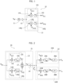
- a conventional RFFE receiver arrangement 10 may comprise:
- the first 13I and second 13Q down-converter branches which may comprise respective mixing and filtering stages, may be configured to apply mixing processing 14I, resp. 14Q, to the RF signal x RF ( t ) and a local oscillator (LO) signal x LO ( t ) component I, resp. Q, the mixing processing 14I, 14Q followed by low-pass filtering processing 16I, resp. 16Q.
- mixing processing 14I, resp. 14Q to the RF signal x RF ( t ) and a local oscillator (LO) signal x LO ( t ) component I, resp. Q
- LO local oscillator
- LO local oscillator
- the oscillator frequency ⁇ LO can either be lower (low-side injection), higher (high-side injection) or equal (direct down-conversion) with respect to the RF frequency ⁇ RF , according to the value used for the intermediate frequency ⁇ IF .
- An RFFE receiver 10 is hence tuned to collect the RF signal x RF ( t ) .
- the analog down-converter branches 131, 13Q may have differential DC offset, gain, and quadrature phase errors. For instance, when mismatches exist between:
- DSP Digital Signal Processor
- solutions employing training signals may partially calibrate the device since, usually, it is difficult to obtain optimal parameters setting.
- the compensation block includes a conjugation block; an adaptive finite impulse response (FIR) filter; and an adder.
- the filter use filter coefficients iteratively updated at least partly in response to a compensated digital signal.
- the filter can have a complex number for at least one, but not all of filter taps, and real numbers for other filter taps.
- the filter can be provided with adaptation step sizes different from filter tap to filter tap.
- the filter can also be provided with an adaptation step size(s) varying over time.
- the filter can also be provided with an adaptation step size(s) divided by the square norm of the compensated signal.
- Document US 2017/126465 A1 discusses methods and apparatuses in which a processor of a transceiver selects one of a real component of a complex signal and an imaginary component of the complex signal.
- the complex signal has IQ imbalance.
- An adaptive filter of the transceiver performs a real multiplication operation using an adaptive filter coefficient and the one of the real component and the imaginary component of the complex signal to generate a complex compensation signal.
- An adder of the transceiver sums the complex signal and the complex compensation signal to generate a compensated signal in which the IQ imbalance is corrected.
- the compensated signal is output for digital processing.
- An object of one or more embodiments is to contribute in providing such an improved solution.
- One or more embodiments may relate to a corresponding computer implemented method.
- One or more embodiments may relate to a corresponding circuit.
- One or more embodiments may relate to a corresponding radio receiver and computer program product.
- One or more embodiments may comprise a tailored modified Symmetric Adaptive Decorrelation algorithm, facilitating to solve the problems of SAD algorithm for wideband receivers, where the I/Q imbalance can have strong variations versus frequency.
- One or more embodiments may comprise an image rejection correction loop.
- One or more embodiments may comprise an adaptive filter stage and detector/correlator stage.
- One or more embodiments may comprise at least one adjustable tap-delay line.
- both adaptive filter stage and detector/correlator stage may employ such an adjustable tap-delay, facilitating to mitigate side effects due to the decorrelation time of clean source signals.
- such an approach can be used likewise in loop-implementations (e.g., in steady-state conditions) as well as in closed form implementations (e.g., to speed-up the initial convergence).
- One or more embodiments may, advantageously:
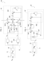
- Figure 2 may be used to provide an equivalent model of an RFFE 10 and following processing, for instance up to baseband signals, comprising for instance:
- the first down-conversion stage 21 may provide input to the subsequent IRC processing stages via interfacing node x in .
- both the first down-conversion stage 21 and the second down-conversion stage 22 are coupled together and may provide inputs to subsequent IRC processing stages via interfacing nodes s ln , i in .
- the first down-conversion stage 21 may comprise an analog I/Q down-converter 13 comprising RF-IF mixers 14I, 14Q coupled to the input node x RF , IF low-pass filters 16I, 16Q coupled to corresponding mixers, an intermediate frequency analog-to-digital converter (briefly, ADC) 18, for instance having sampling period T , an interfacing node x in .
- ADC analog-to-digital converter
- the first down-conversion stage 21 may virtually comprise a combiner 17, for instance a two-real to complex converter, modeling the combination of I/Q signal components interposed between low-pass filters 16I, 16Q in respective branches of the down-converter 13, wherein the combiner 17 may be configured to provide an intermediate frequency signal x IF to the ADC 18.
- the ADC in turn may sample the signal and provide it at the interfacing node x in and/or to the second down-conversion stage 22.
- the second down-conversion stage 22 may be configured for receiving a time-sampled IF signal and to apply processing thereto.
- the second down-conversion stage 22 may comprise:
- the IF-BB mixers 24A, 24B may comprise a pair of complex mixers, typically implemented as numerically controlled oscillators (briefly, NCOs), configured to provide signals for converting to zero-frequency, respectively, the desired signal and the image signal.
- NCOs numerically controlled oscillators
- a spectral contribution X ( ⁇ - ⁇ 0 ), related to a term x ( t ) e j ⁇ 0 t may be indicated as contribution X , centered around ⁇ 0 .
- Figure 2B may be exemplary of a diagram of RF signal contributions S , I , S * and I * in the domain of frequency (or spectral domain), obtained from the baseband equivalents S and I of Figure 2A , respectively related to desired and image signals.
- generated LO signal components have same amplitudes and are in quadrature therebetween, that is one is separated in phase by 90° (or ⁇ /2 ) with respect to the other.
- the filter stages 16I, 16Q have respective impulse responses h IF,I ( t ), h IF,Q ( t ) (and transfer functions H IF,I ( ⁇ ), H IF,Q ( ⁇ ) ) which may be modeled as a nominal intermediate frequency low pass filter (briefly, IF-LPF) having likewise impulse response h IF ( t ) (and transfer function H IF ( ⁇ ) ) on both I and Q signal paths.
- IF-LPF nominal intermediate frequency low pass filter
- baseband mixing 24A, 24B and filtering 26A, 26B performed in the discrete-time domain (after ADC conversion 18) in the second down-conversion stage 22, two baseband signals s BB and i BB (placed around zero-frequency) are obtained, wherein the signal component and the image component do not interfere therebetween.
- I/Q imbalance may be present and may be constant in frequency.
- the desired signal s ( t ) and the image signal i ( t ) may be mixed indistinguishably, introducing unwanted cross-interference.
- I/Q imbalance may lead to crosstalk between wanted signal and image signal, whose amount can be quantified by coefficients ratio K 2 / K 1 * .
- I/Q imbalance here considered is frequency-independent, because this ratio is related only to the (constant) coefficients K 1 and K 2 .
- filter impulse responses h IF,I ( t ), h IF,Q ( t ) (or transfer functions H IF,I ( ⁇ ), H IF,Q ( ⁇ ), in frequency domain) of the respective I/Q signal paths 16I and 16Q may have a mismatch with respect to the impulse response h IF ( t ) (or, similarly, the related transfer function H IF ( ⁇ ) ) of the nominal IF-LPF.
- h I ( t ), h Q ( t ) represent, in time domain, the effect of mismatch on I and Q branches, with respect to the nominal IF-LPF
- H I ( ⁇ ) , H Q ( ⁇ ) represent like mismatch expressed as a function of frequency.
- K 1 ⁇ H I ⁇ + g e ⁇ j ⁇ H Q ⁇ 2
- a ratio K 2 ⁇ / K 1 ⁇ ⁇ ⁇ ⁇ involving mismatch transfer functions K 1 ( ⁇ ) , K 2 ( ⁇ ) may be indicative of the amount of introduced cross-talk.
- This ratio K 2 ⁇ / K 1 ⁇ ⁇ ⁇ may vary, in general, as a function of frequency.
- the I/Q imbalance here considered may be, in general, frequency-dependent.
- a cause of frequency-dependent I/Q imbalance involves time delay ⁇ of "Q" signal path 16Q, for example, with respect to "I" signal path 16I.
- ⁇ time delay
- processing mismatched signals in the IF-BB down-conversion stage 22 may yield baseband signal spectra S BB ( ⁇ ), I BB ( ⁇ ) which, for instance for
- solutions for improving detection and correction of such I/Q imbalance errors may facilitate to achieve a satisfactory level of performance of a signal processing system comprising a wideband receiver 10.
- the ratio K 2 / K 1 ⁇ may be used to quantify the crosstalk phenomenon, in terms of leakage amount.
- Other indicators based on the mismatch coefficients K 1 , K 2 can be used as well.
- the so-called Image Rejection Ratio (briefly, IRR) is a relevant figure of merit of such receiver RFFE architectures 10, providing an indication of the amount of attenuation achieved inside the front-end, relatively to the crosstalk phenomenon.
- Such an IRR parameter may be evaluated at the output of the RF-IF down-conversion stage 21 and expressed as follows:
- One or more embodiments may be particularly suited to deal with I/Q imbalance which varies with respect to frequency, for instance in the second imbalance case scenario.
- one or more embodiments may facilitate extracting a desired signal S from the received RF signal, for instance using decorrelation techniques such as symmetric adaptive decorrelation (briefly, SAD) or blind source separation, as discussed in the following.
- decorrelation techniques such as symmetric adaptive decorrelation (briefly, SAD) or blind source separation, as discussed in the following.
- Modern radio applications may highly benefit from values of IRR of about 80 dB or more, which may be achieved thanks to digital algorithms.
- applying digital decorrelation algorithms after the analog front-end may reduce the effects of I/Q imbalance for narrowband receivers.
- Symmetric Adaptive Decorrelation SAD
- S. Van Gerven and D. Van Compernolle Signal Separation by Symmetric Adaptive Decorrelation: Stability, Convergence, and Uniqueness
- IEEE Trans. Signal Processing vol. 43, no. 7, pp. 1602-1612, July 1995 , may be found suitable for use in narrowband receivers.
- a SAD technique may hardly be a feasible for use with wideband receivers, due to lack of efficiency and effectiveness, e.g. due to the presence of a strongly high frequency-dependent I/Q imbalance.
- the I/Q imbalance can be considered constant versus frequency, as discussed with respect to the first imbalance case, while in a wideband radio receiver the I/Q imbalance can have strong variations as a function of frequency, as discussed with respect to the second (frequency-dependent) imbalance case.
- Figures 2A, 2B and 2C are exemplary diagrams of possible frequency spectra which may be processed as exemplified herein, for instance in a first case of (frequency-independent) I/Q imbalance.
- narrowband may refer to a receiver in which the bandwidth of interest within the RF signal (e.g., suitable bandwidth for successive baseband processing, after down-conversion to IF and analog-to-digital conversion) is (significantly) lower (e.g., by a factor of at least 10) with respect to the analog bandwidth of the system, limited by the IF stage 21. Otherwise, the receiver is considered “wideband”.
- IRC image rejection correction
- one or more embodiments may be useful when a non-zero intermediate frequency is used, e.g. ⁇ IF ⁇ 0 Hz, and when IRC is performed on baseband signals.
- a non-zero intermediate frequency e.g. ⁇ IF ⁇ 0 Hz
- an IRC processing stage may be coupled to baseband stages, which follow a second down-conversion stage 22.
- a (double-branch) crosstalk correction system 30 may comprise:
- the components in Figure 3 may operate partially in the analog domain and partially in the digital domain.
- the ADC stage 18 in the first down-conversion stage 21 may comprise a first ADC coupled to the I signal path filter 16I and a second ADC coupled to the Q signal path filter 16Q and configured to convert from analog to digital the respective I and Q signal components of the down-converted signal x IF ( kT ) .
- crosstalk parasitic effects originating from the analog down-conversion implemented in the first down-conversion stage 21, may be spectrally shifted to baseband in the second down-conversion stage 22, the latter employing digital techniques for the related down-conversion processing of complex signals and, therefore, without introducing further crosstalk contributions.
- crosstalk parasitic effects originating from a direct down-conversion implemented in the first down-conversion stage 21, may directly affect baseband.
- Figure 3A is a diagram exemplary of possible input signal spectra S in , I in for the (double-branch) IRC control loop 36, as discussed in the following.
- output signals from the second down-conversion stage 22, as exemplified in Figure 3A may comprise a superposition of a first signal proportional to the expected/desired signal, e.g. K 1 S, as well as a second signal proportional to a conjugated version of an other/image signal, e.g. K 2 I *.
- the (double-branch) IRC control loop 36 may comprise:
- the first and second adder stages 364A, 364B may comprise circuitry configured to add a plurality of input signals therebetween and to output respective (combined) output signals at respective output nodes s out , i out .
- the feedback branch 368, 369 may be configured to provide coefficients to the first and/or second multiplier stages 362A, 362B as discussed in the following so that a suitable signal may be injected in the signal paths in order to compensate and cancel out unwanted signals due to parasitic cross-interference or I/Q imbalance.
- the feedback branch 368-369 may comprise circuitry, logic, and/or code configured to determine at least one coupling coefficient w indicative of coupling between received signals.
- the at least one complex coefficient w of the multiplier stages 362A, 362B may be computed in the IRC control loop 36, as discussed in the following.
- the feedback branch 368, 369 may comprise:
- mixing and filtering operations in the first down-conversion stage 21 may cause spectral overlap between desired signal and image signal components s ( t ), i ( t ), resulting in non-zero cross-interference, while mixing in the second down-conversion stage 22 may shift these effects to baseband, for instance on signals s BB ( k ), i BB ( k ), which may be applied to IRC control loop 36 input nodes s in , i in .
- the feedback branch correlator/multiplier 368 may receive:
- the at least one complex coupling coefficient w between signals may be determined utilizing decorrelation techniques, and the desired signal may be extracted using the determined coefficient w .
- the update function may depend on an estimated residual correlation between output signals at a given discrete-time moment, for instance output signals s out ( k ) and i out ⁇ k (or, equivalently, i out ( k ) and s out ⁇ k ).
- such residual correlation may be estimated as a result of integrating increments generated from a product of output signals, for instance s out ( k ) i out ( k ).
- Figure 3B is an exemplary diagram of possible frequency spectra of output signals which may be found at output nodes s out , i out , for instance while IRC control loop processing 36 is ongoing.
- a single-branch crosstalk correction system 30' may comprise:
- the single-branch IRC control loop 36' may comprise:
- One or more embodiments may employ a single-branch IRC control loop 36', wherein a single complex signal may be used for the update of the coefficients, estimating residual correlation between the output signal x out ( k ) and it conjugated version x out ⁇ k , thus as a function of integrating increments originated from x out ( k ) 2 .
- Figure 4B is an exemplary diagram of possible frequency spectra of signals which may be processed in a (single-branch) IRC loop processing circuit 36'.
- IRC control circuit 36, 36', 36" may comprise multi-tap processing, which may be particularly suited for compensating imbalance which may vary with frequency (see, for instance, the second imbalance case discussed in the foregoing).
- One or more embodiments as exemplified in Figure 5 may be particularly advantageous to deal with such an input signal x in ( k ), facilitating to deal with a (potentially) frequency-dependent I/Q imbalance.
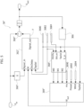
- the multi-tap IRC control loop 36" may comprise:
- the feedback network 368'', 369'' may comprise:
- a Finite-duration Impulse Response (FIR) filter 362" may comprise a filter whose impulse response (that is, the output in response to a Kronecker delta, or Dirac impulse, input) or response to any finite-length input, has a finite duration which may settle to zero in a limited/finite time.
- FIR Finite-duration Impulse Response
- a FIR filter of order N - 1 may have an impulse response which may have a duration equal to a number N of (signal) samples before settling to zero, wherein samples N may be counted from first non-zero element through last non-zero element, with both included.
- the FIR filter 362" may comprise input delay line elements, facilitating to delay the input signal by a given number of samples.
- coefficients W may be applied to a subset of elements belonging to the delay line of the FIR 362'', and decorrelation may be imposed solely for the related delay values.
- the set of coefficients W may be applied to a comb of delay elements, the comb comprising a number N d of delay elements, the delay elements having distance d therebetween, wherein the distance d may be indicated as tap-delay distance or, simply, tap-delay.
- the set of coefficients W may comprise three coefficients w 0 , w 1 , w 2 .
- such a number of coefficients may be particularly suited in satellite radio applications.
- the single-branch IRC structure 36', 36" may comprise a detector/correlator stage 368', 368'', which may perform an estimation of a residual correlation between an output signal x out ( k ) and its complex conjugate version x out ⁇ k .
- the double-branch IRC structure 36 may comprise a detector/correlator stage 368 which may perform an estimation of a residual correlation between a first output signal s out ( k ) and a conjugated version of a second output signal i out ⁇ k , or between a second output signal i out ( k ) and a conjugated version of a first output signal s out ⁇ k .
- correlation estimations can be performed, for instance:
- an update function for the coefficients may also comprise a "block-wise" implementation in the computation of the values of the coefficients in the set of coefficients W .
- Inventors have observed that in a frequency spectrum of a signal output by the IRC control loop 36', 36'', the residual correlation between the positive spectrum and a mirrored version of the negative spectrum, both containing contributions placed around ⁇ IF and derived from S and I *, may be intrinsically combined with the residual correlation between the negative spectrum and a mirrored version of the positive spectrum, both containing contributions placed around ⁇ IF and derived from I and S *, taking advantage from the fact that both the correlation terms facilitate to converge to the same values of the coefficients.
- the result of the computed correlation R, R' may be integrated via a loop filter 369", extending from the detector/correlator 368'' to the adaptive filter 362".
- residual image crosstalk may be estimated and rejected, for instance with DSP techniques operating in the digital domain, by using a correlator stage 368" and an adaptive filter stage 362'', respectively.
- the FIR filter 362" may output a filtered signal x 2 ⁇ ⁇ k which may be subtracted to the IRC input signal x in ( k ), in order to reduce (and virtually remove), on the resulting IRC output signal x out ( k ), the crosstalk effect due to I/Q imbalance in the RFFE 10.
- the IRC control loop 36" may converge to an improved set of filter coefficients W , e.g. optimal in the sense of Least Mean Squares (LMS).
- W Least Mean Squares
- the set of coefficients W of the FIR filter 362" may be updated using the information coming from the loop filter 369", as a function of signals received from the correlator 368".
- One or more embodiments may comprise an automatic gain controller (AGC) stage 366, which may facilitate maintaining a fixed signal level at the input of the detector/correlator 368", in order to have convergence with an almost stable time constant, independently from the input signal power condition.
- AGC automatic gain controller
- wideband receivers may be affected more critically by such a problem and its related effects due to the presence of a strongly frequency-dependent I/Q imbalance.
- the detector/correlator stage 368'' in the IRC control loop 36" may comprise:
- the possibility to use the second tap-delay configuration register 3682 to select a convenient tap-delay distance d value may facilitate performing correlation processing solely for a subset of delay elements, which may be selected accordingly.
- the FIR filter stage 362" ' in the IRC control loop 36" may comprise, for instance:
- the adaptive filter stage 362" ' in the IRC loop 36" may comprise a 3-tap type FIR filter having a "comb" implementation with tap-delay d selected as a function of the value in the second tap-delay configuration register 3682, after activating the FIR implementation of the filter stage 362" as a function of the value in the first tap-selection configuration register 3680.
- the optional block-length configuration register 3684 can be used to configure block-wise calculation of correlation and update of coefficients W , facilitating to increase flexibility of the processing system 36, 36', 36".
- the loop filter 369'' may comprise a set of registers 3690, 3692, 3694 storing respective loop filter parameters ⁇ , PS, Winit.
- the loop filter 369'' in the IRC control loop 36" may comprise, for instance:
- such a solution 36" may facilitate avoiding to select a subset of elements which are separated by a short delay, advantageously, mitigating side effects due to the decorrelation time of (clean) source signals s ( t ), i ( t ) .
- One or more embodiments as exemplified in Figures 8A and 8B may be related to a QPSK application adopting the IRC control loop 36, 36', 36'', wherein the expected (optimum) value for a first FIR coefficient w 1 and a second FIR coefficient w 2 in the set of coefficients W may be zero.
- the loop 36 may converge to sub-optimal values, e.g. due to the side effects related to the decorrelation time of the clean sources, in the detector/correlator 368.
- a first QPSK constellation as exemplified in Figure 8A may have a "slightly confused" distribution, due to the poor signal-to-interferer ratio, generating a high bit error rate.
- the IRC loop 36 may facilitate recovering full system functionality by attenuating the crosstalk effects and providing output signal x out ( k ) having values close to those that may be obtained in the ideal case (see, for instance, the discussion in the foregoing with respect to ideal case).
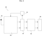
- One or more embodiments as exemplified in Figure 9 may comprise a communication device 90, equipped with circuitry configured to perform an image rejection correction method as discussed herein.
- such a communication device 90 e.g. an RF receiver, may comprise:
- the communication device 90 may be in a transceiver, for example, and may be utilized for receiving satellite, terrestrial or cable television or radio signals, or any RF signal requiring a frequency down-conversion through analog I/Q mixer.
- the receiver 90 may be operable to receive satellite, terrestrial or cable television or radio signals, down-convert and process the signals for communication to a display device and/or a set of loudspeakers.
- the RFFE 93 may comprise one or more RF receive (Rx) and transmit (Tx) paths for receiving signals from a satellite system, cable TV head-end, and/or terrestrial TV antennas, for example.
- Rx receive
- Tx transmit
- the RFFE may further comprise impedance matching elements, low-noise amplifiers (LNAs), power amplifiers, variable gain amplifiers, and filters, for example.
- LNAs low-noise amplifiers
- the RFFE stage 93 may thus be operable to receive, amplify, and filter RF signals before communicating them to, e.g., the baseband processor 98.
- the ADC 94 may comprise a wideband ADC and may be operable to convert received analog signals to digital signals.
- the processing circuitry 96 may comprise a compensation circuit 30, 30' comprising an IRC loop circuit 36, 36', 36'' as discussed in the foregoing, for instance with respect to Figure 5 , or it may comprise general processing means and a memory configured to perform the method of imbalance correction 36, 36', 36" according to one or more embodiments, e.g. via software.
- the process may be performed entirely in the digital circuitry without using complex analog circuitry.
- the communication device processing circuitry 96 may comprise a memory, e.g. a programmable memory module that may be operable to store software and data, for example, for the operation of the receiver device 90.
- the memory may store the adaptive filter coefficients computed in the IRC control loop in the compensation circuit.
- One or more embodiments may found use in any communication receiver 90 in which signal processing employs a frequency down-conversion stage based on an analog I/Q mixer, regardless of the information content of the received signal (broadcasting services, networks, astronomy, etc.), the modulation technique that is adopted (AM, FM, OFDM, QPSK, etc.) and the physical nature of the transmission channel, which can be based on a radio link (terrestrial or via satellite) or on a medium-guided approach (metal cable, waveguide, optical fiber, etc.).
- a radio link terrestrial or via satellite
- a medium-guided approach metal cable, waveguide, optical fiber, etc.
- some examples of such communication receivers may be used for broadcasting services (television, radio, positioning systems: GNSS and others, etc.) or for network services (point-to-point, point-to-multipoint, switched networks for telephonic signals, digital data, etc.).
- broadcasting services television, radio, positioning systems: GNSS and others, etc.
- network services point-to-point, point-to-multipoint, switched networks for telephonic signals, digital data, etc.
- One or more embodiments may improve performances of, among others, communication receivers for terrestrial radio wideband receivers, satellite radio wideband receivers, satellite GNSS receivers.
Landscapes
- Engineering & Computer Science (AREA)
- Computer Networks & Wireless Communication (AREA)
- Signal Processing (AREA)
- Physics & Mathematics (AREA)
- Computer Hardware Design (AREA)
- Mathematical Physics (AREA)
- Power Engineering (AREA)
- Noise Elimination (AREA)
- Superheterodyne Receivers (AREA)
Claims (12)
- Verfahren (30, 30'), das von einer Schaltung durchgeführt wird, Folgendes umfassend:- Empfangen eines Eingangssignals (xin, Xin ), das mindestens eine Sequenz von Eingangsdatenabtastungen umfasst, die durch eine Abtastperiode (T) dazwischen getrennt sind, wobei das Eingangssignal (xin, Xin ) eine gewünschte Signalkomponente und eine ihr überlagerte Störsignalkomponente umfasst,- Anwenden einer Störkomponentenschätzungsverarbeitung (36, 36', 36") auf das Eingangssignal (xin, Xin ), um als Ergebnis ein gefiltertes Signal (F) zu erhalten, das eine Sequenz von gefilterten Datenabtastungen umfasst,- Subtrahieren (364A, 364B, 364', 364") des gefilterten Signals (F) von dem Eingangssignal (xin, Xin ) und Erhalten eines Ausgangssignals (xout , Xout ), das eine Sequenz von Ausgangsdatenabtastungen umfasst, als Ergebnis,wobei die Störkomponentenschätzungsverarbeitung (36, 36', 36") Folgendes umfasst:a) Anwenden einer Konjugationsverarbeitung (360A, 360B, 360', 360") auf das Eingangssignal (xin, Xin ), wodurch eine konjugierte Version des Eingangssignals (xin, Xin ) bereitgestellt wird,b) Berechnen von mindestens einem Wert eines adaptiven Signalverarbeitungskoeffizienten (w; w 0, w 1, w 2),c) Anwenden einer adaptiven Signalverarbeitung (362A, 362B, 362', 362") auf die konjugierte Version des Eingangssignals (xin, Xin ) unter Verwendung mindestens eines adaptiven Verarbeitungskoeffizienten (w; w 0, w 1, w 2), wobei als Ergebnis das gefilterte Signal (F) erhalten wird,wobei das Berechnen von mindestens einem Wert eines adaptiven Signalverarbeitungskoeffizienten (w; w 0, w 1, w 2) Folgendes umfasst:i) Durchführen einer Korrelationsverarbeitung (368, 368', 368") zwischen der Sequenz von Ausgangsdatenabtastwerten des Ausgangssignals (xout , Xout ) und einer konjugierten Version der Sequenz von Ausgangsdatenabtastwerten des Ausgangssignals (xout , Xout ) und Erhalten einer Sequenz von Schätzungen der Restkorrelation als Ergebnis,ii) Anwenden einer Integrationsverarbeitung (369, 369', 369") auf die Sequenz der bereitgestellten Schätzungen der Restkorrelation (368, 368', 368"), wobei die Integrationsverarbeitung einen Integrationsschrittparameter (µ) und mindestens einen Startpunktparameter (Winit) umfasst,iii) Erhalten von mindestens einem berechneten adaptiven Signalverarbeitungskoeffizienten (w; w 0, w 1, w 2) als Ergebnis des Anwendens der Integrationsverarbeitung (369, 369', 369"),wobei das Anwenden der adaptiven Signalverarbeitung (362A, 362B, 362', 362") adaptive Filterverarbeitung mit endlicher Impulsantwort, FIR (362"), umfasst, die das Berechnen einer gewichteten Summe einer konjugierten Version von Datenwerten in der Sequenz von Eingangsdatenabtastwerten, die in dem Eingangssignal (xin, Xin ) enthalten sind, unter Verwendung des mindestens einen adaptiven Verarbeitungskoeffizienten (w 0, w 1, w 2) als Gewichte der gewichteten Summe umfasst,wobei:- die adaptive FIR-Filterverarbeitung das Anwenden des mindestens einen adaptiven Verarbeitungskoeffizienten (w 0, w 1, w 2) auf eine Teilmenge von Elementen umfasst, die zu einer Eingangsverzögerungsleitung der FIR (362") gehören, auf eine zugehörige Untergruppe von Verzögerungswerten;- das Durchführen einer Korrelationsverarbeitung (368, 368', 368") und das Anwenden einer Integrationsverarbeitung (369, 369', 369") jeweils das Berechnen und Integrieren von Schätzungen der Restkorrelation bei Verzögerungswerten der zugehörigen Teilmenge von Verzögerungswerten umfassen, und- die adaptiven FIR-Filterkoeffizienten (w 0, w 1, w 2) auf einen Kamm von Elementen angewandt werden, die zu der Eingangsverzögerungsleitung der FIR (362") gehören, wobei der Kamm eine Anzahl Nd von Verzögerungselementen umfasst,wobei die Verzögerungselemente einen Abstandswert haben, der ein Vielfaches der Abtastperiode (T) mit einem Faktor d ist,wobei das Verfahren weiter Folgendes umfasst:- Bereitstellen mindestens eines zweiten Konfigurationsregisters (3682), das zum Speichern von Indizes von Verzögerungselementen in dem Satz von Verzögerungselementen der Verzögerungsleitung konfiguriert ist, und- Auswählen einer Teilmenge von Verzögerungselementen in der Menge von Verzögerungselementen der Verzögerungsleitung als Funktion der in dem mindestens einen zweiten Konfigurationsregister (3682) gespeicherten Indizes.
- Verfahren nach Anspruch 1, wobei das Anwenden einer adaptiven Signalverarbeitung (362A, 362B, 362', 362") das Anwenden einer adaptiven FIR-Filterverarbeitung zweiter Ordnung oder einer adaptiven FIR-Filterverarbeitung mit drei Abgriffen umfasst.
- Verfahren nach Anspruch 1 oder Anspruch 2, wobei der Abstandswert mehr als das Zehnfache in Bezug auf die Abtastperiode (T) beträgt.
- Verfahren nach einem der vorhergehenden Ansprüche, wobei das Anwenden der Integrationsverarbeitung (369, 369', 369") das Anwenden der Schleifenfilterverarbeitung (369) auf die Sequenz von Schätzungen der bereitgestellten Restkorrelation (368, 368', 368") umfasst.
- Verfahren nach einem der vorhergehenden Ansprüche, wobei das Anwenden der Integrationsverarbeitung (369, 369', 369") mindestens einen der folgenden Schritte umfasst:- Bereitstellen eines ersten Integrationsparameterregisters (3690), das zum Speichern eines Wertes des Integrationsschrittparameters (µ) konfiguriert ist,- Bereitstellen mindestens eines zweiten Integrationsparameterregisters (3694), das konfiguriert ist, um einen Wert des mindestens einen Startpunktparameters (Winit) zu speichern, und eines dritten Integrationsparameterregisters (3692), das konfiguriert ist, um die Integrationsverarbeitung (369, 369', 369") zu aktivieren (PS, 3692), um den Wert des mindestens einen Startpunktparameters (Winit) zu verwenden.
- Verfahren nach einem der vorhergehenden Ansprüche, wobei das Berechnen mindestens eines Wertes des mindestens einen adaptiven Verarbeitungskoeffizienten (w; w 0, w 1, w 2) das Anwenden der automatischen Verstärkungsregelung, AGC, auf das Ausgangssignal (xout , Xout ) umfasst.
- Verfahren nach einem der vorhergehenden Ansprüche, wobei die Durchführung einer Korrelationsverarbeitung (368, 368', 368") zwischen der Sequenz von Ausgangsdatenabtastwerten des Ausgangssignals (xout , Xout ) und einer konjugierten Version der Sequenz von Ausgangsdatenabtastwerten des Ausgangssignals (xout , Xout ) die Durchführung einer blockartigen Korrelation einer Anzahl von benachbarten Datenabtastwerten umfasst, die einen Block mit der Blocklänge L von Datenabtastwerten bilden.
- Verfahren nach Anspruch 7, y wobei die Blocklänge L in Abhängigkeit von einem Längenwert ausgewählt wird, der in einem Konfigurationsregister (3684) gespeichert ist.
- Schaltung, die Folgendes umfasst:- einen Eingangsknoten (xin, Xin), der so konfiguriert ist, dass er mindestens ein Eingangssignal (xin, Xin ) empfängt, das mindestens eine Sequenz von Eingangsdatenabtastungen umfasst, wobei das Eingangssignal (xin, Xin ) eine gewünschte Signalkomponente und eine dieser überlagerte Störsignalkomponente umfasst, wobei Eingangsdatenabtastwerte in der Sequenz von Eingangsdatenabtastwerten durch eine Abtastperiode (T) dazwischen getrennt sind,- eine Signalverarbeitungsschaltung (30, 30', 96), die so konfiguriert ist, dass sie auf das empfangene mindestens eine Eingangssignal (xin, Xin ) mit dem Verfahren nach einem der Ansprüche 1 bis 8 eine Verarbeitung zur Beseitigung von Störkomponenten (36, 36', 36") anwendet.
- Schaltung nach Anspruch 9, wobei die Signalverarbeitungsschaltung (30, 30', 96) weiter eine komplexe Abwärtswandlerschaltung (22) umfasst, die Folgendes umfasst:- einen ersten Mischerzweig (22A), der einen gemeinsamen Eingangsknoten (xin, Xin ) umfasst, der so konfiguriert ist, dass er mindestens ein Signal (xin, Xin ) empfängt, einen ersten digitalen Mischer (24A), einen ersten digitalen Tiefpassfilter (26A), einen ersten Basisbanddezimator (28A) mit Dezimierungsfaktor M und einen ersten Schnittstellenknoten (sin ), wobei der erste Schnittstellenknoten so konfiguriert ist, dass er eine erste Signalkomponente (sin ) bereitstellt, und- einen zweiten Mischerzweig (22B), der einen gemeinsamen Eingangsknoten (xin, Xin ) umfasst, der so konfiguriert ist, dass er mindestens ein Signal (xin, Xin ) empfängt, einen zweiten digitalen Mischer (24B), einen zweiten digitalen Tiefpassfilter (26B), einen zweiten Basisbanddezimator (28B) mit Dezimierungsfaktor M und einen zweiten Schnittstellenknoten (iin ), wobei der zweite Schnittstellenknoten so konfiguriert ist, dass er eine zweite Signalkomponente (iin ) bereitstellt, und- eine IRC-Regelschleife (36), die so konfiguriert ist, dass sie eine Störkomponentenentfernungsverarbeitung (36) mit dem Verfahren nach einem der Ansprüche 1 bis 6 auf die erste Signalkomponente (sin ) und auf die zweite Signalkomponente (iin ) anwendet.
- Hochfrequenz-Empfangsvorrichtung (90), Folgendes umfassend:- eine Antenne (92), die so konfiguriert ist, dass sie ein Hochfrequenzsignal empfängt,- ein Hochfrequenz-Frontend (93), das mit der Antenne gekoppelt ist, wobei das Hochfrequenz-Frontend so konfiguriert ist, dass es das Hochfrequenzsignal an einem Eingangsknoten (xRF ) empfängt und das Hochfrequenzsignal einer Abwärtsumwandlung unterzieht, wobei das Hochfrequenz-Frontend (93) einen ersten Ausgangsknoten (xIF ) aufweist und so konfiguriert ist, dass es ein Zwischenfrequenzsignal, IF, als Ergebnis der Abwärtsumwandlung an dem ersten Ausgangsknoten (xIF ) bereitstellt,- eine Analog-Digital-Wandler-Stufe (94), ADC, die einen Eingangsknoten aufweist, der mit dem ersten Ausgangsknoten (xIF ) gekoppelt ist, und einen zweiten Ausgangsknoten, wobei die ADC-Stufe (94) so konfiguriert ist, dass sie das IF-Signal von dem ersten Ausgangsknoten (xIF ) empfängt, eine Signalabtastung darauf anwendet und eine abgetastete Sequenz von Datenabtastungen des IF-Signals an dem zweiten Ausgangsknoten bereitstellt,- eine Schaltung (96) nach Anspruch 9 oder 10, bei welcher der Eingangsknoten (xin ) mit dem zweiten Ausgangsknoten der ADC-Stufe (94) gekoppelt ist, wobei die Schaltung (96) so konfiguriert ist, dass sie das IF-Signal als Eingangssignal empfängt.
- Computerprogrammprodukt, das Befehle umfasst, die, wenn das Programm von einem Computer ausgeführt wird, den Computer veranlassen, die Schritte des Verfahrens nach einem der Ansprüche 1 bis 8 auszuführen.
Applications Claiming Priority (1)
| Application Number | Priority Date | Filing Date | Title |
|---|---|---|---|
| IT102019000024298A IT201900024298A1 (it) | 2019-12-17 | 2019-12-17 | Procedimento di compensazione di reiezione di immagine per i/q down-conversion in ricevitori a radiofrequenza, circuito, dispositivo ricevitore a radio frequenza e prodotto informatico corrispondenti |
Publications (2)
| Publication Number | Publication Date |
|---|---|
| EP3840318A1 EP3840318A1 (de) | 2021-06-23 |
| EP3840318B1 true EP3840318B1 (de) | 2024-02-21 |
Family
ID=70009309
Family Applications (1)
| Application Number | Title | Priority Date | Filing Date |
|---|---|---|---|
| EP20213682.6A Active EP3840318B1 (de) | 2019-12-17 | 2020-12-14 | I/q-abwärtsumsetzung mit spiegelfrequenzkompensation |
Country Status (4)
| Country | Link |
|---|---|
| US (1) | US11855830B2 (de) |
| EP (1) | EP3840318B1 (de) |
| CN (1) | CN112994653B (de) |
| IT (1) | IT201900024298A1 (de) |
Families Citing this family (1)
| Publication number | Priority date | Publication date | Assignee | Title |
|---|---|---|---|---|
| US10819540B2 (en) * | 2018-09-11 | 2020-10-27 | Hughes Network Systems, Llc | Radio frequency impairments compensator for broadband quadrature-conversion architectures |
Family Cites Families (7)
| Publication number | Priority date | Publication date | Assignee | Title |
|---|---|---|---|---|
| US8649464B2 (en) * | 2010-08-10 | 2014-02-11 | Sony Corporation | Quadrature receiver and method of compensating for I/Q imbalance using a calibration signal |
| US9148328B2 (en) * | 2010-10-29 | 2015-09-29 | Samsung Electronics Co., Ltd. | Digital I/Q imbalance compensation in a quadrature receiver |
| US8363712B2 (en) * | 2011-01-06 | 2013-01-29 | Analog Devices, Inc. | Apparatus and method for adaptive I/Q imbalance compensation |
| US8509298B2 (en) * | 2011-01-06 | 2013-08-13 | Analog Devices, Inc. | Apparatus and method for adaptive I/Q imbalance compensation |
| DE112011104692B4 (de) * | 2011-01-06 | 2017-08-24 | Analog Devices Inc. | Vorrichtung und Verfahren zur adaptiven I/Q-Asymmetriekompensation |
| CN102739578A (zh) * | 2011-03-31 | 2012-10-17 | 广东明家科技股份有限公司 | 一种回波干扰抑制方法、装置及终端 |
| US9712369B2 (en) * | 2015-11-03 | 2017-07-18 | Samsung Electronics Co., Ltd | Method and apparatus for low-complexity frequency dependent IQ imbalance compensation |
-
2019
- 2019-12-17 IT IT102019000024298A patent/IT201900024298A1/it unknown
-
2020
- 2020-12-14 EP EP20213682.6A patent/EP3840318B1/de active Active
- 2020-12-15 US US17/123,003 patent/US11855830B2/en active Active
- 2020-12-17 CN CN202011493887.4A patent/CN112994653B/zh active Active
Also Published As
| Publication number | Publication date |
|---|---|
| IT201900024298A1 (it) | 2021-06-17 |
| CN112994653A (zh) | 2021-06-18 |
| CN112994653B (zh) | 2024-08-16 |
| US11855830B2 (en) | 2023-12-26 |
| EP3840318A1 (de) | 2021-06-23 |
| US20210194746A1 (en) | 2021-06-24 |
Similar Documents
| Publication | Publication Date | Title |
|---|---|---|
| US10541840B2 (en) | Systems and methods for adaptively-tuned digital self-interference cancellation | |
| US9680674B2 (en) | I/Q calibration techniques | |
| US7995973B2 (en) | Own transmitter interference tolerant transceiver and receiving methods | |
| US8855580B2 (en) | Methods and apparatus for reducing own-transmitter interference in low-IF and zero-IF receivers | |
| US7151917B2 (en) | Apparatus and method for deriving a digital image correction factor in a receiver | |
| US8509298B2 (en) | Apparatus and method for adaptive I/Q imbalance compensation | |
| US8265584B2 (en) | Providing image rejection calibration for a receiver | |
| EP2237413B1 (de) | Kompensatoreinheit und Kompensationsverfahren für I/Q-Unsymmetriefehler | |
| US8363712B2 (en) | Apparatus and method for adaptive I/Q imbalance compensation | |
| US20050070239A1 (en) | Apparatus and method for digital image correction in a receiver | |
| US20170126465A1 (en) | Method and apparatus for low-complexity frequency dependent iq imbalance compensation | |
| US20070097271A1 (en) | Receiver with image rejection calibration at an undesired picture carrier and method therefor | |
| EP3840318B1 (de) | I/q-abwärtsumsetzung mit spiegelfrequenzkompensation | |
| US9641361B2 (en) | Sub-sampling receiver | |
| US9036740B2 (en) | Performing image rejection on bandpass signals | |
| US10122568B2 (en) | Digital compensation of IQ coupling in communication receivers | |
| JP3698996B2 (ja) | 通信システムにおける受信機 | |
| US7672655B1 (en) | Frequency-selective and adaptive I/Q mismatch digital compensation | |
| US9287912B2 (en) | Multimode receiver with complex filter | |
| WO2012094087A1 (en) | Apparatus and method for adaptive i/q imbalance compensation | |
| KR20130095216A (ko) | 블라인드 채널 추정 알고리즘을 사용하는 신호 처리 유닛 및 수신기 장치의 동작 방법 | |
| RU2289885C2 (ru) | Способ выравнивания каналов многоканальной приемной системы (варианты) | |
| US20100296502A1 (en) | I-q mismatch compensation |
Legal Events
| Date | Code | Title | Description |
|---|---|---|---|
| PUAI | Public reference made under article 153(3) epc to a published international application that has entered the european phase |
Free format text: ORIGINAL CODE: 0009012 |
|
| STAA | Information on the status of an ep patent application or granted ep patent |
Free format text: STATUS: THE APPLICATION HAS BEEN PUBLISHED |
|
| AK | Designated contracting states |
Kind code of ref document: A1 Designated state(s): AL AT BE BG CH CY CZ DE DK EE ES FI FR GB GR HR HU IE IS IT LI LT LU LV MC MK MT NL NO PL PT RO RS SE SI SK SM TR |
|
| STAA | Information on the status of an ep patent application or granted ep patent |
Free format text: STATUS: REQUEST FOR EXAMINATION WAS MADE |
|
| 17P | Request for examination filed |
Effective date: 20211203 |
|
| RBV | Designated contracting states (corrected) |
Designated state(s): AL AT BE BG CH CY CZ DE DK EE ES FI FR GB GR HR HU IE IS IT LI LT LU LV MC MK MT NL NO PL PT RO RS SE SI SK SM TR |
|
| STAA | Information on the status of an ep patent application or granted ep patent |
Free format text: STATUS: EXAMINATION IS IN PROGRESS |
|
| 17Q | First examination report despatched |
Effective date: 20230208 |
|
| RIC1 | Information provided on ipc code assigned before grant |
Ipc: H04L 27/00 20060101ALN20230814BHEP Ipc: H04L 27/38 20060101AFI20230814BHEP |
|
| GRAP | Despatch of communication of intention to grant a patent |
Free format text: ORIGINAL CODE: EPIDOSNIGR1 |
|
| RIC1 | Information provided on ipc code assigned before grant |
Ipc: H04L 27/00 20060101ALN20230828BHEP Ipc: H04L 27/38 20060101AFI20230828BHEP |
|
| STAA | Information on the status of an ep patent application or granted ep patent |
Free format text: STATUS: GRANT OF PATENT IS INTENDED |
|
| INTG | Intention to grant announced |
Effective date: 20231005 |
|
| GRAS | Grant fee paid |
Free format text: ORIGINAL CODE: EPIDOSNIGR3 |
|
| GRAA | (expected) grant |
Free format text: ORIGINAL CODE: 0009210 |
|
| STAA | Information on the status of an ep patent application or granted ep patent |
Free format text: STATUS: THE PATENT HAS BEEN GRANTED |
|
| AK | Designated contracting states |
Kind code of ref document: B1 Designated state(s): AL AT BE BG CH CY CZ DE DK EE ES FI FR GB GR HR HU IE IS IT LI LT LU LV MC MK MT NL NO PL PT RO RS SE SI SK SM TR |
|
| REG | Reference to a national code |
Ref country code: GB Ref legal event code: FG4D |
|
| REG | Reference to a national code |
Ref country code: CH Ref legal event code: EP |
|
| REG | Reference to a national code |
Ref country code: DE Ref legal event code: R096 Ref document number: 602020025981 Country of ref document: DE |
|
| REG | Reference to a national code |
Ref country code: IE Ref legal event code: FG4D |
|
| REG | Reference to a national code |
Ref country code: LT Ref legal event code: MG9D |
|
| REG | Reference to a national code |
Ref country code: NL Ref legal event code: MP Effective date: 20240221 |
|
| PG25 | Lapsed in a contracting state [announced via postgrant information from national office to epo] |
Ref country code: IS Free format text: LAPSE BECAUSE OF FAILURE TO SUBMIT A TRANSLATION OF THE DESCRIPTION OR TO PAY THE FEE WITHIN THE PRESCRIBED TIME-LIMIT Effective date: 20240621 |
|
| PG25 | Lapsed in a contracting state [announced via postgrant information from national office to epo] |
Ref country code: LT Free format text: LAPSE BECAUSE OF FAILURE TO SUBMIT A TRANSLATION OF THE DESCRIPTION OR TO PAY THE FEE WITHIN THE PRESCRIBED TIME-LIMIT Effective date: 20240221 |
|
| PG25 | Lapsed in a contracting state [announced via postgrant information from national office to epo] |
Ref country code: GR Free format text: LAPSE BECAUSE OF FAILURE TO SUBMIT A TRANSLATION OF THE DESCRIPTION OR TO PAY THE FEE WITHIN THE PRESCRIBED TIME-LIMIT Effective date: 20240522 |
|
| REG | Reference to a national code |
Ref country code: AT Ref legal event code: MK05 Ref document number: 1660087 Country of ref document: AT Kind code of ref document: T Effective date: 20240221 |
|
| PG25 | Lapsed in a contracting state [announced via postgrant information from national office to epo] |
Ref country code: HR Free format text: LAPSE BECAUSE OF FAILURE TO SUBMIT A TRANSLATION OF THE DESCRIPTION OR TO PAY THE FEE WITHIN THE PRESCRIBED TIME-LIMIT Effective date: 20240221 Ref country code: RS Free format text: LAPSE BECAUSE OF FAILURE TO SUBMIT A TRANSLATION OF THE DESCRIPTION OR TO PAY THE FEE WITHIN THE PRESCRIBED TIME-LIMIT Effective date: 20240521 Ref country code: NL Free format text: LAPSE BECAUSE OF FAILURE TO SUBMIT A TRANSLATION OF THE DESCRIPTION OR TO PAY THE FEE WITHIN THE PRESCRIBED TIME-LIMIT Effective date: 20240221 |
|
| PG25 | Lapsed in a contracting state [announced via postgrant information from national office to epo] |
Ref country code: ES Free format text: LAPSE BECAUSE OF FAILURE TO SUBMIT A TRANSLATION OF THE DESCRIPTION OR TO PAY THE FEE WITHIN THE PRESCRIBED TIME-LIMIT Effective date: 20240221 |
|
| PG25 | Lapsed in a contracting state [announced via postgrant information from national office to epo] |
Ref country code: AT Free format text: LAPSE BECAUSE OF FAILURE TO SUBMIT A TRANSLATION OF THE DESCRIPTION OR TO PAY THE FEE WITHIN THE PRESCRIBED TIME-LIMIT Effective date: 20240221 |
|
| PG25 | Lapsed in a contracting state [announced via postgrant information from national office to epo] |
Ref country code: RS Free format text: LAPSE BECAUSE OF FAILURE TO SUBMIT A TRANSLATION OF THE DESCRIPTION OR TO PAY THE FEE WITHIN THE PRESCRIBED TIME-LIMIT Effective date: 20240521 Ref country code: NO Free format text: LAPSE BECAUSE OF FAILURE TO SUBMIT A TRANSLATION OF THE DESCRIPTION OR TO PAY THE FEE WITHIN THE PRESCRIBED TIME-LIMIT Effective date: 20240521 Ref country code: NL Free format text: LAPSE BECAUSE OF FAILURE TO SUBMIT A TRANSLATION OF THE DESCRIPTION OR TO PAY THE FEE WITHIN THE PRESCRIBED TIME-LIMIT Effective date: 20240221 Ref country code: LT Free format text: LAPSE BECAUSE OF FAILURE TO SUBMIT A TRANSLATION OF THE DESCRIPTION OR TO PAY THE FEE WITHIN THE PRESCRIBED TIME-LIMIT Effective date: 20240221 Ref country code: IS Free format text: LAPSE BECAUSE OF FAILURE TO SUBMIT A TRANSLATION OF THE DESCRIPTION OR TO PAY THE FEE WITHIN THE PRESCRIBED TIME-LIMIT Effective date: 20240621 Ref country code: HR Free format text: LAPSE BECAUSE OF FAILURE TO SUBMIT A TRANSLATION OF THE DESCRIPTION OR TO PAY THE FEE WITHIN THE PRESCRIBED TIME-LIMIT Effective date: 20240221 Ref country code: GR Free format text: LAPSE BECAUSE OF FAILURE TO SUBMIT A TRANSLATION OF THE DESCRIPTION OR TO PAY THE FEE WITHIN THE PRESCRIBED TIME-LIMIT Effective date: 20240522 Ref country code: FI Free format text: LAPSE BECAUSE OF FAILURE TO SUBMIT A TRANSLATION OF THE DESCRIPTION OR TO PAY THE FEE WITHIN THE PRESCRIBED TIME-LIMIT Effective date: 20240221 Ref country code: ES Free format text: LAPSE BECAUSE OF FAILURE TO SUBMIT A TRANSLATION OF THE DESCRIPTION OR TO PAY THE FEE WITHIN THE PRESCRIBED TIME-LIMIT Effective date: 20240221 Ref country code: BG Free format text: LAPSE BECAUSE OF FAILURE TO SUBMIT A TRANSLATION OF THE DESCRIPTION OR TO PAY THE FEE WITHIN THE PRESCRIBED TIME-LIMIT Effective date: 20240221 Ref country code: AT Free format text: LAPSE BECAUSE OF FAILURE TO SUBMIT A TRANSLATION OF THE DESCRIPTION OR TO PAY THE FEE WITHIN THE PRESCRIBED TIME-LIMIT Effective date: 20240221 |
|
| PG25 | Lapsed in a contracting state [announced via postgrant information from national office to epo] |
Ref country code: PT Free format text: LAPSE BECAUSE OF FAILURE TO SUBMIT A TRANSLATION OF THE DESCRIPTION OR TO PAY THE FEE WITHIN THE PRESCRIBED TIME-LIMIT Effective date: 20240621 Ref country code: PL Free format text: LAPSE BECAUSE OF FAILURE TO SUBMIT A TRANSLATION OF THE DESCRIPTION OR TO PAY THE FEE WITHIN THE PRESCRIBED TIME-LIMIT Effective date: 20240221 |
|
| PG25 | Lapsed in a contracting state [announced via postgrant information from national office to epo] |
Ref country code: SE Free format text: LAPSE BECAUSE OF FAILURE TO SUBMIT A TRANSLATION OF THE DESCRIPTION OR TO PAY THE FEE WITHIN THE PRESCRIBED TIME-LIMIT Effective date: 20240221 Ref country code: PT Free format text: LAPSE BECAUSE OF FAILURE TO SUBMIT A TRANSLATION OF THE DESCRIPTION OR TO PAY THE FEE WITHIN THE PRESCRIBED TIME-LIMIT Effective date: 20240621 Ref country code: PL Free format text: LAPSE BECAUSE OF FAILURE TO SUBMIT A TRANSLATION OF THE DESCRIPTION OR TO PAY THE FEE WITHIN THE PRESCRIBED TIME-LIMIT Effective date: 20240221 Ref country code: LV Free format text: LAPSE BECAUSE OF FAILURE TO SUBMIT A TRANSLATION OF THE DESCRIPTION OR TO PAY THE FEE WITHIN THE PRESCRIBED TIME-LIMIT Effective date: 20240221 |
|
| PG25 | Lapsed in a contracting state [announced via postgrant information from national office to epo] |
Ref country code: DK Free format text: LAPSE BECAUSE OF FAILURE TO SUBMIT A TRANSLATION OF THE DESCRIPTION OR TO PAY THE FEE WITHIN THE PRESCRIBED TIME-LIMIT Effective date: 20240221 |
|
| PG25 | Lapsed in a contracting state [announced via postgrant information from national office to epo] |
Ref country code: SM Free format text: LAPSE BECAUSE OF FAILURE TO SUBMIT A TRANSLATION OF THE DESCRIPTION OR TO PAY THE FEE WITHIN THE PRESCRIBED TIME-LIMIT Effective date: 20240221 |
|
| PG25 | Lapsed in a contracting state [announced via postgrant information from national office to epo] |
Ref country code: CZ Free format text: LAPSE BECAUSE OF FAILURE TO SUBMIT A TRANSLATION OF THE DESCRIPTION OR TO PAY THE FEE WITHIN THE PRESCRIBED TIME-LIMIT Effective date: 20240221 Ref country code: EE Free format text: LAPSE BECAUSE OF FAILURE TO SUBMIT A TRANSLATION OF THE DESCRIPTION OR TO PAY THE FEE WITHIN THE PRESCRIBED TIME-LIMIT Effective date: 20240221 |
|
| PG25 | Lapsed in a contracting state [announced via postgrant information from national office to epo] |
Ref country code: SK Free format text: LAPSE BECAUSE OF FAILURE TO SUBMIT A TRANSLATION OF THE DESCRIPTION OR TO PAY THE FEE WITHIN THE PRESCRIBED TIME-LIMIT Effective date: 20240221 |
|
| PG25 | Lapsed in a contracting state [announced via postgrant information from national office to epo] |
Ref country code: SM Free format text: LAPSE BECAUSE OF FAILURE TO SUBMIT A TRANSLATION OF THE DESCRIPTION OR TO PAY THE FEE WITHIN THE PRESCRIBED TIME-LIMIT Effective date: 20240221 Ref country code: SK Free format text: LAPSE BECAUSE OF FAILURE TO SUBMIT A TRANSLATION OF THE DESCRIPTION OR TO PAY THE FEE WITHIN THE PRESCRIBED TIME-LIMIT Effective date: 20240221 Ref country code: RO Free format text: LAPSE BECAUSE OF FAILURE TO SUBMIT A TRANSLATION OF THE DESCRIPTION OR TO PAY THE FEE WITHIN THE PRESCRIBED TIME-LIMIT Effective date: 20240221 Ref country code: EE Free format text: LAPSE BECAUSE OF FAILURE TO SUBMIT A TRANSLATION OF THE DESCRIPTION OR TO PAY THE FEE WITHIN THE PRESCRIBED TIME-LIMIT Effective date: 20240221 Ref country code: DK Free format text: LAPSE BECAUSE OF FAILURE TO SUBMIT A TRANSLATION OF THE DESCRIPTION OR TO PAY THE FEE WITHIN THE PRESCRIBED TIME-LIMIT Effective date: 20240221 Ref country code: CZ Free format text: LAPSE BECAUSE OF FAILURE TO SUBMIT A TRANSLATION OF THE DESCRIPTION OR TO PAY THE FEE WITHIN THE PRESCRIBED TIME-LIMIT Effective date: 20240221 |
|
| REG | Reference to a national code |
Ref country code: DE Ref legal event code: R097 Ref document number: 602020025981 Country of ref document: DE |
|
| PG25 | Lapsed in a contracting state [announced via postgrant information from national office to epo] |
Ref country code: IT Free format text: LAPSE BECAUSE OF FAILURE TO SUBMIT A TRANSLATION OF THE DESCRIPTION OR TO PAY THE FEE WITHIN THE PRESCRIBED TIME-LIMIT Effective date: 20240221 |
|
| PLBE | No opposition filed within time limit |
Free format text: ORIGINAL CODE: 0009261 |
|
| STAA | Information on the status of an ep patent application or granted ep patent |
Free format text: STATUS: NO OPPOSITION FILED WITHIN TIME LIMIT |
|
| PG25 | Lapsed in a contracting state [announced via postgrant information from national office to epo] |
Ref country code: IT Free format text: LAPSE BECAUSE OF FAILURE TO SUBMIT A TRANSLATION OF THE DESCRIPTION OR TO PAY THE FEE WITHIN THE PRESCRIBED TIME-LIMIT Effective date: 20240221 |
|
| 26N | No opposition filed |
Effective date: 20241122 |
|
| PG25 | Lapsed in a contracting state [announced via postgrant information from national office to epo] |
Ref country code: SI Free format text: LAPSE BECAUSE OF FAILURE TO SUBMIT A TRANSLATION OF THE DESCRIPTION OR TO PAY THE FEE WITHIN THE PRESCRIBED TIME-LIMIT Effective date: 20240221 |
|
| PG25 | Lapsed in a contracting state [announced via postgrant information from national office to epo] |
Ref country code: MC Free format text: LAPSE BECAUSE OF FAILURE TO SUBMIT A TRANSLATION OF THE DESCRIPTION OR TO PAY THE FEE WITHIN THE PRESCRIBED TIME-LIMIT Effective date: 20240221 |
|
| REG | Reference to a national code |
Ref country code: CH Ref legal event code: PL |
|
| PG25 | Lapsed in a contracting state [announced via postgrant information from national office to epo] |
Ref country code: LU Free format text: LAPSE BECAUSE OF NON-PAYMENT OF DUE FEES Effective date: 20241214 |
|
| GBPC | Gb: european patent ceased through non-payment of renewal fee |
Effective date: 20241214 |
|
| REG | Reference to a national code |
Ref country code: BE Ref legal event code: MM Effective date: 20241231 |
|
| PG25 | Lapsed in a contracting state [announced via postgrant information from national office to epo] |
Ref country code: GB Free format text: LAPSE BECAUSE OF NON-PAYMENT OF DUE FEES Effective date: 20241214 Ref country code: BE Free format text: LAPSE BECAUSE OF NON-PAYMENT OF DUE FEES Effective date: 20241231 |
|
| PG25 | Lapsed in a contracting state [announced via postgrant information from national office to epo] |
Ref country code: FR Free format text: LAPSE BECAUSE OF NON-PAYMENT OF DUE FEES Effective date: 20241231 |
|
| PG25 | Lapsed in a contracting state [announced via postgrant information from national office to epo] |
Ref country code: CH Free format text: LAPSE BECAUSE OF NON-PAYMENT OF DUE FEES Effective date: 20241231 |
|
| PG25 | Lapsed in a contracting state [announced via postgrant information from national office to epo] |
Ref country code: IE Free format text: LAPSE BECAUSE OF NON-PAYMENT OF DUE FEES Effective date: 20241214 |
|
| PGFP | Annual fee paid to national office [announced via postgrant information from national office to epo] |
Ref country code: DE Payment date: 20251126 Year of fee payment: 6 |