EP3840542A1 - Support de composant stratifié compact avec puce d'extrémité avant et circuit d'adaptation d'impédance pour communication d'antenne - Google Patents
Support de composant stratifié compact avec puce d'extrémité avant et circuit d'adaptation d'impédance pour communication d'antenne Download PDFInfo
- Publication number
- EP3840542A1 EP3840542A1 EP19217655.0A EP19217655A EP3840542A1 EP 3840542 A1 EP3840542 A1 EP 3840542A1 EP 19217655 A EP19217655 A EP 19217655A EP 3840542 A1 EP3840542 A1 EP 3840542A1
- Authority
- EP
- European Patent Office
- Prior art keywords
- component carrier
- stack
- antenna
- impedance matching
- end chip
- Prior art date
- Legal status (The legal status is an assumption and is not a legal conclusion. Google has not performed a legal analysis and makes no representation as to the accuracy of the status listed.)
- Pending
Links
Images


Classifications
-
- H—ELECTRICITY
- H10—SEMICONDUCTOR DEVICES; ELECTRIC SOLID-STATE DEVICES NOT OTHERWISE PROVIDED FOR
- H10W—GENERIC PACKAGES, INTERCONNECTIONS, CONNECTORS OR OTHER CONSTRUCTIONAL DETAILS OF DEVICES COVERED BY CLASS H10
- H10W70/00—Package substrates; Interposers; Redistribution layers [RDL]
- H10W70/60—Insulating or insulated package substrates; Interposers; Redistribution layers
- H10W70/62—Insulating or insulated package substrates; Interposers; Redistribution layers characterised by their interconnections
- H10W70/65—Shapes or dispositions of interconnections
-
- H—ELECTRICITY
- H01—ELECTRIC ELEMENTS
- H01Q—ANTENNAS, i.e. RADIO AERIALS
- H01Q1/00—Details of, or arrangements associated with, antennas
- H01Q1/12—Supports; Mounting means
- H01Q1/22—Supports; Mounting means by structural association with other equipment or articles
- H01Q1/2283—Supports; Mounting means by structural association with other equipment or articles mounted in or on the surface of a semiconductor substrate as a chip-type antenna or integrated with other components into an IC package
-
- H—ELECTRICITY
- H01—ELECTRIC ELEMENTS
- H01Q—ANTENNAS, i.e. RADIO AERIALS
- H01Q1/00—Details of, or arrangements associated with, antennas
- H01Q1/12—Supports; Mounting means
- H01Q1/22—Supports; Mounting means by structural association with other equipment or articles
- H01Q1/2291—Supports; Mounting means by structural association with other equipment or articles used in Bluetooth® or Wi-Fi® devices of Wireless Local Area Networks [WLAN]
-
- H—ELECTRICITY
- H01—ELECTRIC ELEMENTS
- H01Q—ANTENNAS, i.e. RADIO AERIALS
- H01Q1/00—Details of, or arrangements associated with, antennas
- H01Q1/12—Supports; Mounting means
- H01Q1/22—Supports; Mounting means by structural association with other equipment or articles
- H01Q1/24—Supports; Mounting means by structural association with other equipment or articles with receiving set
- H01Q1/241—Supports; Mounting means by structural association with other equipment or articles with receiving set used in mobile communications, e.g. GSM
-
- H—ELECTRICITY
- H01—ELECTRIC ELEMENTS
- H01Q—ANTENNAS, i.e. RADIO AERIALS
- H01Q23/00—Antennas with active circuits or circuit elements integrated within them or attached to them
-
- H—ELECTRICITY
- H01—ELECTRIC ELEMENTS
- H01Q—ANTENNAS, i.e. RADIO AERIALS
- H01Q5/00—Arrangements for simultaneous operation of antennas on two or more different wavebands, e.g. dual-band or multi-band arrangements
- H01Q5/30—Arrangements for providing operation on different wavebands
- H01Q5/307—Individual or coupled radiating elements, each element being fed in an unspecified way
- H01Q5/314—Individual or coupled radiating elements, each element being fed in an unspecified way using frequency dependent circuits or components, e.g. trap circuits or capacitors
- H01Q5/335—Individual or coupled radiating elements, each element being fed in an unspecified way using frequency dependent circuits or components, e.g. trap circuits or capacitors at the feed, e.g. for impedance matching
-
- H—ELECTRICITY
- H04—ELECTRIC COMMUNICATION TECHNIQUE
- H04B—TRANSMISSION
- H04B1/00—Details of transmission systems, not covered by a single one of groups H04B3/00 - H04B13/00; Details of transmission systems not characterised by the medium used for transmission
- H04B1/02—Transmitters
- H04B1/04—Circuits
-
- H—ELECTRICITY
- H05—ELECTRIC TECHNIQUES NOT OTHERWISE PROVIDED FOR
- H05K—PRINTED CIRCUITS; CASINGS OR CONSTRUCTIONAL DETAILS OF ELECTRIC APPARATUS; MANUFACTURE OF ASSEMBLAGES OF ELECTRICAL COMPONENTS
- H05K1/00—Printed circuits
- H05K1/02—Details
- H05K1/0213—Electrical arrangements not otherwise provided for
- H05K1/0237—High frequency adaptations
- H05K1/025—Impedance arrangements, e.g. impedance matching, reduction of parasitic impedance
-
- H—ELECTRICITY
- H05—ELECTRIC TECHNIQUES NOT OTHERWISE PROVIDED FOR
- H05K—PRINTED CIRCUITS; CASINGS OR CONSTRUCTIONAL DETAILS OF ELECTRIC APPARATUS; MANUFACTURE OF ASSEMBLAGES OF ELECTRICAL COMPONENTS
- H05K1/00—Printed circuits
- H05K1/18—Printed circuits structurally associated with non-printed electric components
- H05K1/182—Printed circuits structurally associated with non-printed electric components associated with components mounted in printed circuit boards [PCB], e.g. insert-mounted components [IMC]
- H05K1/183—Printed circuits structurally associated with non-printed electric components associated with components mounted in printed circuit boards [PCB], e.g. insert-mounted components [IMC] associated with components mounted in and supported by recessed areas of the PCBs
-
- H—ELECTRICITY
- H05—ELECTRIC TECHNIQUES NOT OTHERWISE PROVIDED FOR
- H05K—PRINTED CIRCUITS; CASINGS OR CONSTRUCTIONAL DETAILS OF ELECTRIC APPARATUS; MANUFACTURE OF ASSEMBLAGES OF ELECTRICAL COMPONENTS
- H05K1/00—Printed circuits
- H05K1/18—Printed circuits structurally associated with non-printed electric components
- H05K1/182—Printed circuits structurally associated with non-printed electric components associated with components mounted in printed circuit boards [PCB], e.g. insert-mounted components [IMC]
- H05K1/185—Printed circuits structurally associated with non-printed electric components associated with components mounted in printed circuit boards [PCB], e.g. insert-mounted components [IMC] associated with components encapsulated in the insulating substrate of the PCBs; associated with components incorporated in internal layers of multilayer circuit boards
- H05K1/188—Printed circuits structurally associated with non-printed electric components associated with components mounted in printed circuit boards [PCB], e.g. insert-mounted components [IMC] associated with components encapsulated in the insulating substrate of the PCBs; associated with components incorporated in internal layers of multilayer circuit boards manufactured by mounting on or attaching to a structure having a conductive layer, e.g. a metal foil, such that the terminals of the component are connected to or adjacent to the conductive layer before embedding, and by using the conductive layer, which is patterned after embedding, at least partially for connecting the component
-
- H—ELECTRICITY
- H10—SEMICONDUCTOR DEVICES; ELECTRIC SOLID-STATE DEVICES NOT OTHERWISE PROVIDED FOR
- H10W—GENERIC PACKAGES, INTERCONNECTIONS, CONNECTORS OR OTHER CONSTRUCTIONAL DETAILS OF DEVICES COVERED BY CLASS H10
- H10W42/00—Arrangements for protection of devices
- H10W42/20—Arrangements for protection of devices protecting against electromagnetic or particle radiation, e.g. light, X-rays, gamma-rays or electrons
-
- H—ELECTRICITY
- H10—SEMICONDUCTOR DEVICES; ELECTRIC SOLID-STATE DEVICES NOT OTHERWISE PROVIDED FOR
- H10W—GENERIC PACKAGES, INTERCONNECTIONS, CONNECTORS OR OTHER CONSTRUCTIONAL DETAILS OF DEVICES COVERED BY CLASS H10
- H10W44/00—Electrical arrangements for controlling or matching impedance
- H10W44/20—Electrical arrangements for controlling or matching impedance at high-frequency [HF] or radio frequency [RF]
-
- H—ELECTRICITY
- H10—SEMICONDUCTOR DEVICES; ELECTRIC SOLID-STATE DEVICES NOT OTHERWISE PROVIDED FOR
- H10W—GENERIC PACKAGES, INTERCONNECTIONS, CONNECTORS OR OTHER CONSTRUCTIONAL DETAILS OF DEVICES COVERED BY CLASS H10
- H10W70/00—Package substrates; Interposers; Redistribution layers [RDL]
- H10W70/01—Manufacture or treatment
- H10W70/05—Manufacture or treatment of insulating or insulated package substrates, or of interposers, or of redistribution layers
-
- H—ELECTRICITY
- H10—SEMICONDUCTOR DEVICES; ELECTRIC SOLID-STATE DEVICES NOT OTHERWISE PROVIDED FOR
- H10W—GENERIC PACKAGES, INTERCONNECTIONS, CONNECTORS OR OTHER CONSTRUCTIONAL DETAILS OF DEVICES COVERED BY CLASS H10
- H10W70/00—Package substrates; Interposers; Redistribution layers [RDL]
- H10W70/60—Insulating or insulated package substrates; Interposers; Redistribution layers
- H10W70/67—Insulating or insulated package substrates; Interposers; Redistribution layers characterised by their insulating layers or insulating parts
- H10W70/68—Shapes or dispositions thereof
- H10W70/685—Shapes or dispositions thereof comprising multiple insulating layers
-
- H—ELECTRICITY
- H05—ELECTRIC TECHNIQUES NOT OTHERWISE PROVIDED FOR
- H05K—PRINTED CIRCUITS; CASINGS OR CONSTRUCTIONAL DETAILS OF ELECTRIC APPARATUS; MANUFACTURE OF ASSEMBLAGES OF ELECTRICAL COMPONENTS
- H05K1/00—Printed circuits
- H05K1/02—Details
- H05K1/0213—Electrical arrangements not otherwise provided for
- H05K1/0216—Reduction of cross-talk, noise or electromagnetic interference
- H05K1/0218—Reduction of cross-talk, noise or electromagnetic interference by printed shielding conductors, ground planes or power plane
- H05K1/0219—Printed shielding conductors for shielding around or between signal conductors, e.g. coplanar or coaxial printed shielding conductors
- H05K1/0222—Printed shielding conductors for shielding around or between signal conductors, e.g. coplanar or coaxial printed shielding conductors for shielding around a single via or around a group of vias, e.g. coaxial vias or vias surrounded by a grounded via fence
-
- H—ELECTRICITY
- H05—ELECTRIC TECHNIQUES NOT OTHERWISE PROVIDED FOR
- H05K—PRINTED CIRCUITS; CASINGS OR CONSTRUCTIONAL DETAILS OF ELECTRIC APPARATUS; MANUFACTURE OF ASSEMBLAGES OF ELECTRICAL COMPONENTS
- H05K1/00—Printed circuits
- H05K1/02—Details
- H05K1/0213—Electrical arrangements not otherwise provided for
- H05K1/0237—High frequency adaptations
- H05K1/0243—Printed circuits associated with mounted high frequency components
-
- H—ELECTRICITY
- H05—ELECTRIC TECHNIQUES NOT OTHERWISE PROVIDED FOR
- H05K—PRINTED CIRCUITS; CASINGS OR CONSTRUCTIONAL DETAILS OF ELECTRIC APPARATUS; MANUFACTURE OF ASSEMBLAGES OF ELECTRICAL COMPONENTS
- H05K2201/00—Indexing scheme relating to printed circuits covered by H05K1/00
- H05K2201/07—Electric details
- H05K2201/0707—Shielding
- H05K2201/0723—Shielding provided by an inner layer of PCB
-
- H—ELECTRICITY
- H05—ELECTRIC TECHNIQUES NOT OTHERWISE PROVIDED FOR
- H05K—PRINTED CIRCUITS; CASINGS OR CONSTRUCTIONAL DETAILS OF ELECTRIC APPARATUS; MANUFACTURE OF ASSEMBLAGES OF ELECTRICAL COMPONENTS
- H05K2201/00—Indexing scheme relating to printed circuits covered by H05K1/00
- H05K2201/09—Shape and layout
- H05K2201/09209—Shape and layout details of conductors
- H05K2201/09372—Pads and lands
- H05K2201/09481—Via in pad; Pad over filled via
-
- H—ELECTRICITY
- H05—ELECTRIC TECHNIQUES NOT OTHERWISE PROVIDED FOR
- H05K—PRINTED CIRCUITS; CASINGS OR CONSTRUCTIONAL DETAILS OF ELECTRIC APPARATUS; MANUFACTURE OF ASSEMBLAGES OF ELECTRICAL COMPONENTS
- H05K2201/00—Indexing scheme relating to printed circuits covered by H05K1/00
- H05K2201/09—Shape and layout
- H05K2201/09209—Shape and layout details of conductors
- H05K2201/09654—Shape and layout details of conductors covering at least two types of conductors provided for in H05K2201/09218 - H05K2201/095
- H05K2201/09809—Coaxial layout
-
- H—ELECTRICITY
- H05—ELECTRIC TECHNIQUES NOT OTHERWISE PROVIDED FOR
- H05K—PRINTED CIRCUITS; CASINGS OR CONSTRUCTIONAL DETAILS OF ELECTRIC APPARATUS; MANUFACTURE OF ASSEMBLAGES OF ELECTRICAL COMPONENTS
- H05K2201/00—Indexing scheme relating to printed circuits covered by H05K1/00
- H05K2201/10—Details of components or other objects attached to or integrated in a printed circuit board
- H05K2201/10007—Types of components
- H05K2201/10098—Components for radio transmission, e.g. radio frequency identification [RFID] tag, printed or non-printed antennas
-
- H—ELECTRICITY
- H05—ELECTRIC TECHNIQUES NOT OTHERWISE PROVIDED FOR
- H05K—PRINTED CIRCUITS; CASINGS OR CONSTRUCTIONAL DETAILS OF ELECTRIC APPARATUS; MANUFACTURE OF ASSEMBLAGES OF ELECTRICAL COMPONENTS
- H05K2201/00—Indexing scheme relating to printed circuits covered by H05K1/00
- H05K2201/10—Details of components or other objects attached to or integrated in a printed circuit board
- H05K2201/10431—Details of mounted components
- H05K2201/10507—Involving several components
- H05K2201/10545—Related components mounted on both sides of the PCB
-
- H—ELECTRICITY
- H05—ELECTRIC TECHNIQUES NOT OTHERWISE PROVIDED FOR
- H05K—PRINTED CIRCUITS; CASINGS OR CONSTRUCTIONAL DETAILS OF ELECTRIC APPARATUS; MANUFACTURE OF ASSEMBLAGES OF ELECTRICAL COMPONENTS
- H05K3/00—Apparatus or processes for manufacturing printed circuits
- H05K3/46—Manufacturing multilayer circuits
- H05K3/4644—Manufacturing multilayer circuits by building the multilayer layer by layer, i.e. build-up multilayer circuits
-
- H—ELECTRICITY
- H05—ELECTRIC TECHNIQUES NOT OTHERWISE PROVIDED FOR
- H05K—PRINTED CIRCUITS; CASINGS OR CONSTRUCTIONAL DETAILS OF ELECTRIC APPARATUS; MANUFACTURE OF ASSEMBLAGES OF ELECTRICAL COMPONENTS
- H05K3/00—Apparatus or processes for manufacturing printed circuits
- H05K3/46—Manufacturing multilayer circuits
- H05K3/4697—Manufacturing multilayer circuits having cavities, e.g. for mounting components
-
- H—ELECTRICITY
- H10—SEMICONDUCTOR DEVICES; ELECTRIC SOLID-STATE DEVICES NOT OTHERWISE PROVIDED FOR
- H10W—GENERIC PACKAGES, INTERCONNECTIONS, CONNECTORS OR OTHER CONSTRUCTIONAL DETAILS OF DEVICES COVERED BY CLASS H10
- H10W44/00—Electrical arrangements for controlling or matching impedance
- H10W44/20—Electrical arrangements for controlling or matching impedance at high-frequency [HF] or radio frequency [RF]
- H10W44/241—Electrical arrangements for controlling or matching impedance at high-frequency [HF] or radio frequency [RF] for passive devices or passive elements
- H10W44/248—Electrical arrangements for controlling or matching impedance at high-frequency [HF] or radio frequency [RF] for passive devices or passive elements for antennas
-
- H—ELECTRICITY
- H10—SEMICONDUCTOR DEVICES; ELECTRIC SOLID-STATE DEVICES NOT OTHERWISE PROVIDED FOR
- H10W—GENERIC PACKAGES, INTERCONNECTIONS, CONNECTORS OR OTHER CONSTRUCTIONAL DETAILS OF DEVICES COVERED BY CLASS H10
- H10W70/00—Package substrates; Interposers; Redistribution layers [RDL]
- H10W70/60—Insulating or insulated package substrates; Interposers; Redistribution layers
- H10W70/67—Insulating or insulated package substrates; Interposers; Redistribution layers characterised by their insulating layers or insulating parts
- H10W70/68—Shapes or dispositions thereof
- H10W70/682—Shapes or dispositions thereof comprising holes having chips therein
-
- H—ELECTRICITY
- H10—SEMICONDUCTOR DEVICES; ELECTRIC SOLID-STATE DEVICES NOT OTHERWISE PROVIDED FOR
- H10W—GENERIC PACKAGES, INTERCONNECTIONS, CONNECTORS OR OTHER CONSTRUCTIONAL DETAILS OF DEVICES COVERED BY CLASS H10
- H10W72/00—Interconnections or connectors in packages
- H10W72/851—Dispositions of multiple connectors or interconnections
- H10W72/874—On different surfaces
-
- H—ELECTRICITY
- H10—SEMICONDUCTOR DEVICES; ELECTRIC SOLID-STATE DEVICES NOT OTHERWISE PROVIDED FOR
- H10W—GENERIC PACKAGES, INTERCONNECTIONS, CONNECTORS OR OTHER CONSTRUCTIONAL DETAILS OF DEVICES COVERED BY CLASS H10
- H10W90/00—Package configurations
- H10W90/701—Package configurations characterised by the relative positions of pads or connectors relative to package parts
- H10W90/721—Package configurations characterised by the relative positions of pads or connectors relative to package parts of bump connectors
- H10W90/724—Package configurations characterised by the relative positions of pads or connectors relative to package parts of bump connectors between a chip and a stacked insulating package substrate, interposer or RDL
Definitions
- the invention relates to a component carrier, to a smart device, to a method of manufacturing a component carrier, and to a method use.
- component carriers equipped with one or more electronic components and increasing miniaturization of such electronic components as well as a rising number of electronic components to be mounted on the component carriers such as printed circuit boards
- increasingly more powerful array-like components or packages having several electronic components are being employed, which have a plurality of contacts or connections, with ever smaller spacing between these contacts. Removal of heat generated by such electronic components and the component carrier itself during operation becomes an increasing issue.
- component carriers shall be mechanically robust and electrically reliable so as to be operable even under harsh conditions.
- conventional component carriers for high frequency communication may be space consuming and may involve significant signal loss.
- a component carrier In order to achieve the object defined above, a component carrier, a smart device, a method of manufacturing a component carrier, and a method of use according to the independent claims are provided.
- a component carrier comprising a laminated stack comprising at least one electrically conductive layer structure and/or at least one electrically insulating layer structure, a front end chip on and/or in the stack and extending at least up to a main surface of the stack, an antenna interface on an opposing other main surface of the stack, and an impedance matching circuitry in the stack and arranged vertically between the front end chip and the antenna interface.
- a smart device which comprises a component carrier having the above mentioned features.
- a component carrier having the above mentioned features may be used for a high-frequency application and/or for a high-power application.
- a method of manufacturing a component carrier comprises laminating a stack comprising at least one electrically conductive layer structure and/or at least one electrically insulating layer structure, mounting a front end chip on and/or in the stack to extend at least up to a main surface of the stack, arranging an antenna interface on an opposing other main surface of the stack, and arranging an impedance matching circuitry in the stack vertically between the front end chip and the antenna interface.
- component carrier may particularly denote any support structure which is capable of accommodating one or more components thereon and/or therein for providing mechanical support and/or electrical connectivity.
- a component carrier may be configured as a mechanical and/or electronic carrier for components.
- a component carrier may be one of a printed circuit board, an organic interposer, and an IC (integrated circuit) substrate.
- a component carrier may also be a hybrid board combining different ones of the above mentioned types of component carriers.
- layer structure may particularly denote a continuous layer, a patterned layer or a plurality of non-consecutive islands within a common plane.
- the term "high-frequency application” may particularly denote a task fulfilled by the component carrier or to which the component carrier contributes, wherein the task may relate to the handling of a radio frequency signal.
- a radio or high-frequency signal may be an electric or electromagnetic signal propagating along a wiring structure of a component carrier in a range of frequencies used for communications or other signals.
- a radio frequency (RF) signal may for example have a frequency in the range between 10 MHz and 300 GHz.
- the term "front end chip” may particularly denote an electronic component (more particularly a semiconductor chip) configured for carrying out front end processing tasks of a high frequency application, in particular communication application.
- a front end chip may include at least one filter (for instance a high pass filter, a low pass filter and/or a bandpass filter), a mixer for mixing signals and/or an ADC (analog-digital-converter).
- the front end chip may process a front end signal for example in the analog domain.
- the term "antenna interface” may particularly denote an interface at which an antenna is connected or is connectable. Such an antenna may be provided for receiving and/or transmitting electromagnetic radiation including information concerning the content of a signal to be communicated between the component carrier and an electronic periphery.
- the antenna may be directly assembled with the antenna interface, i.e. may be integrally formed with the antenna interface or may even constitute the antenna interface.
- the antenna interface only provides an interface for connecting an external antenna, for instance an antenna provided in form of an antenna component or connected to the antenna interface via a socket-plug-connection.
- the term "impedance matching circuitry” may particularly denote a semiconductor chip or a multi-constituent circuitry which provides for a matching of the impedances of the front end chip and of an antenna connected or to be connected to the antenna interface.
- the resistance, the capacitance and/or the inductance between front end chip and antenna may be matched to each other by the impedance matching circuitry.
- an impedance matching may be achieved with copper circuitry (see for instance reference signs 104, 116 in Figure 7 ), passive components (see for example capacitors 160, inductors 162 and resistors; while the former are shown in Figure 8 , the latter are not shown in Figure 8 but may be implemented as well, or integrated passive devices (IPD, see for example reference sign 112 in Figure 1 ).
- copper circuitry see for instance reference signs 104, 116 in Figure 7
- passive components see for example capacitors 160, inductors 162 and resistors; while the former are shown in Figure 8 , the latter are not shown in Figure 8 but may be implemented as well, or integrated passive devices (IPD, see for example reference sign 112 in Figure 1 ).
- smart device may particularly denote an electronic device with smart electronics capability.
- a smart device may be an electronic device which may be connected to other devices or networks via different wireless protocols (such as Bluetooth, Zigbee, NFC, Wi-Fi, Li-Fi, etc.) that can operate interactively and autonomously.
- the smart device may be one of the group consisting of a smartphone, a tablet, a phablet, a laptop, a game console, a smartcard, a smart doorbell, a smart lock, a small refrigerator, a smart watch, a smart band, a smart key chain, a smart speaker, a smart node, an IoT (Internet of Things) device, etc.
- IoT Internet of Things
- a component carrier such as a printed circuit board (PCB) or an IC (integrated circuit) substrate
- PCB printed circuit board
- IC integrated circuit
- a very short connection path may be obtained by the mentioned vertically stacked constituents. This may result in a high signal quality, low loss and strong suppression of artefacts.
- such a component carrier may have a very flat and also laterally compact configuration allowing to integrate it even under limited space requirements, such as within the casing of a smart device.
- an integrated ground layer which may serve as part of an antenna, may be basically a copper layer additionally enabling a better thermal energy distribution through the whole module or component carrier. Therefore, thermal energy may be efficiently guided from the interior of the (for example PCB-type) component carrier to the ambient environment.
- the thermal energy may be coupled to a motherboard (for instance of PCB-type) on the one hand side, and the antenna configuration (especially a ground layer) may distribute the heat homogeneously over the whole module or component carrier and may also contribute to transfer the heat to the ambient.
- the front end chip is surface-mounted on the stack or is accommodated in a cavity of the stack extending up to the main surface.
- the electric connection of the front end chip to an electronic environment is very simple.
- Such a configuration also results in a flat design.
- a front end chip may be easily substituted by another front end chip (for instance to support another frequency regime or in terms of a redesign of the component carrier).
- the component carrier comprises an antenna connected to the antenna interface.
- the antenna may form an integral part of the component carrier and may be integrally formed with the antenna interface.
- the antenna is a patterned electrically conductive material or an antenna component.
- the antenna is formed as one of the electrically conductive layer structures of the stack on an upper main surface thereof. This allows manufacturing an integrally connected antenna with low effort and compact configuration.
- the antenna may be a separate component which may be for instance mounted on top of the stack, such as an antenna chip.
- patterned conductive layers which may constitute said antenna or part thereof, may be produced in a way that very smooth surfaces are obtained, which enables high signal transmission with very low losses.
- An appropriate production technique is mSAP (modified semi-additive processing) which enables to obtain highly defined copper paths with low surface roughness.
- mSAP modified semi-additive processing
- the manufacturing of the module or component carrier may be done in a way to achieve low surface roughness which results in a better signal performance especially for higher frequencies.
- the antenna interface is a socket for connecting an antenna, in particular via an electric cable, via a flexible component carrier (for instance PCB) configuration (for instance in terms of mobile phone connections, etc).
- the component carrier may comprise the antenna which may be equipped with a plug being connectable or connected to the socket, in particular in a substitutable way.
- the antenna may be a separate component which may be attached to the antenna interface, for instance in a detachable way.
- the component carrier may be flexibly connected with different antenna types. This provides a high flexibility of supporting different applications.
- the impedance matching circuitry is configured for matching an impedance between the front end chip and an antenna connected to the antenna interface.
- Impedance matching may denote an electronic design according to which an input impedance of an electrical load or an output impedance of its corresponding signal source may be adjusted to obtain a proper power transfer or reduce undesired signal reflection.
- the impedance matching circuitry is a Balun.
- a Balun (“balanced to unbalanced") may be denoted as an electric circuitry that converts between a balanced signal and an unbalanced signal.
- a Balun may also include circuitry that transforms impedances.
- a Balun is a specifically powerful implementation of an impedance matching circuit.
- the antenna structure, the impedance matching circuitry and the front end chip are vertically stacked, in particular electrically connected with each other by vertical through-connections.
- vertically stacking antenna, impedance matching circuit and front end chip very short electric connection paths, which may in particular extend substantially vertically, may be obtained.
- Low surface roughness may also enable improved signal transmission with low losses.
- Both, short connection paths and copper surfaces with low surface roughness may allow for an enhanced signal transport with low losses. Thus, this may ensure a low loss signal transport and may simultaneously allow obtaining a highly compact configuration of the component carrier.
- front end chip, impedance matching circuitry and antenna interface (optionally including an antenna) may also be horizontally aligned to obtain a highly compact configuration.
- the component carrier comprises a shielding structure for shielding electromagnetic radiation between the impedance matching circuitry and/or the frontage upon the one hand and the antenna interface on the other hand.
- the shielding structure may be arranged on and/or in the stack and may in particular be integrally formed with the stack.
- such a shielding structure may be configured for absorbing and/or reflecting electromagnetic radiation (such as high frequency radiation) in a propagation path between impedance matching circuitry and antenna.
- the shielding structure comprises at least one substantially continuous magnetic layer and/or at least one substantially continuous electrically conductive layer.
- a magnetic layer laminated into the stack of the component carrier is a simply manufacturable and highly efficient way of preventing the propagation of electromagnetic radiation between antenna and front end chip.
- a ferrite material or nanocrystalline magnetic particles or metal flake-based materials may be used for such a shielding structure.
- appropriate materials for the shielding structure are nano-crystalline soft magnetic materials like nano-crystalline alloys with the basic composition FeCu M SiB in which M can be one of the elements Nb, Ta, Mo, W or Zr.
- amorphous metals like for example ferrite may be used for the shielding structure.
- metal-flake based materials may be based on conductive solid fillers such as metallic powders, metal flakes, metal-coated fibers, metal nanowires and different carbon-based materials as carbon black, graphite, and graphene or carbon nanotubes into a matrix.
- Deposited copper (for instance in form of one or more layers) may be used for ultra-high frequency applications.
- a sufficiently thick copper layer or the like may be implemented between antenna and front end chip for shielding electromagnetic radiation from propagating therebetween.
- a substantially continuous shielding layer which may however be traversed by one or more small through-holes for guiding electric signals between the antenna, the impedance matching circuitry and/or the front end chip.
- the component carrier comprises a via-in-via.
- a via-in-via structure may be configured for transporting an electric signal in a shielded fashion.
- a via-in-via configuration may function in a similar way as a coax cable on PCB scale which provides excellent shielding capabilities of signals conducted through the inner via of the via-in-via configuration.
- the exterior (for instance hollow cylindrical) via may then accomplish the shielding function.
- the impedance matching circuitry is configured as an impedance matching component (in particular an impedance matching semiconductor chip).
- a semiconductor die providing an impedance matching functionality can be embedded as a hole in the stack.
- the impedance matching circuitry may be an arrangement of circuit elements interconnected within the stack by the electrically conductive layer structure to thereby achieve an impedance matching function.
- a plurality of passive elements such capacitor elements, resistor elements, inductor elements, etc.
- the at least one electrically insulating layer structure comprises a high-frequency dielectric.
- the term "high-frequency dielectric” may particularly denote an electrically insulating material which has low loss properties when a high-frequency or radiofrequency signal propagates from or to an antenna structure in the direct environment of the high-frequency dielectric.
- the high-frequency dielectric may have a lower loss than standard prepreg material of a stack of component carrier material.
- RO3003TM material as commercialized by the company Rogers Corporation, can be used as high-frequency dielectric.
- high-frequency dielectric material may have a dissipation factor of not more than 0.005, in particular of not more than 0.003, more particularly not more than 0.0015, at 10 GHz.
- the mentioned high frequency circuit materials may be for example ceramic-filled PTFE (polytetrafluoroethylene) composites.
- the high-frequency dielectric is a high-frequency capable prepreg, FR4 or ABF material.
- Such a high-frequency dielectric material may have a relative permeability ⁇ r in a range between 1.01 and 4.
- one or more electrically insulating layer structures may be configured as a high-frequency dielectric.
- the main surface (relating to the front end chip) of the component carrier is mounted on a mounting base of the smart device.
- a mounting base may be a further component carrier such as a printed circuit board (PCB).
- PCB printed circuit board
- a side wall of the stack comprises an electrically conductive connection structure for mounting and connecting the component carrier on a mounting base, in particular of a smart device.
- a side wall plating may be produced, i.e. an electrically conductive structure on a side wall of the component carrier. This side wall may be in electric contact with the front end chip.
- the component carrier is configured as one of the group consisting of a transceiver, a transmitter and a receiver.
- the antenna of the component carrier only receives electromagnetic radiation from an environment, only emits electromagnetic radiation to an environment or carries out both tasks, i.e. emitting and receiving.
- the component carrier is configured for communicating via a mobile communication network, a short-range network, LoRaWan, Sigfox, Zigbee, Bluetooth, or WiFi.
- a mobile communication network a short-range network
- LoRaWan a short-range network
- Sigfox a short-range network
- Zigbee a short-range network
- Bluetooth a short-range network
- WiFi Wireless Fidelity
- the communication according to other wireless communication standards can be enabled by the component carrier as well.
- the stack comprises at least one through hole being at least partially filled with an electrically conductive filling medium (such as plated copper) for electrically connecting opposing main surfaces of the stack.
- an electrically conductive filling medium such as plated copper
- the through hole may be formed by laser processing or by mechanically drilling.
- the filling medium may be copper which may be inserted into the through hole for example by electroless deposition and/or plating.
- a short vertical connection path between the two opposing main surfaces of the component carrier may be obtained which also suppresses signal loss.
- a short vertical connection path may also enable good temperature dissipation and temperature guidance towards the ambient environment. By that, signal loss may also be suppressed.
- the component carrier is used for 5G (or higher).
- Mobile wireless communication according to the 5G standard involves high-frequency transmission with a high transmitted data volume per time and therefore requires excellent properties in terms of high-frequency behavior.
- a component carrier according to an exemplary embodiment of the invention meets these demanding requirements.
- Fifth generation (5G) networks feature an increased mobile data rate, in particular significantly above 100 Mb/s.
- Fifth generation communication networks can experience superior network transmission fidelity when implementing a component carrier according to an exemplary embodiment of the invention.
- the component carrier is used for high-frequency applications above 1 GHz, in particular about 300 GHz.
- signal transmission is particularly sensitive to stub caused artefacts.
- the high RF performance of component carriers according to exemplary embodiments of the invention allows low loss signal transmission even with such high-frequency values.
- the component carrier comprises a stack of at least one electrically insulating layer structure and at least one electrically conductive layer structure.
- the component carrier may be a laminate of the mentioned electrically insulating layer structure(s) and electrically conductive layer structure(s), in particular formed by applying mechanical pressure and/or thermal energy.
- the mentioned stack may provide a plate-shaped component carrier capable of providing a large mounting surface for further components and being nevertheless very thin and compact.
- layer structure may particularly denote a continuous layer, a patterned layer or a plurality of non-consecutive islands within a common plane.
- a surface roughness of such a layer structure may be low, in order to obtain proper signal transmission at low loss in particular at high frequencies.
- the component carrier is shaped as a plate. This contributes to the compact design, wherein the component carrier nevertheless provides a large basis for mounting components thereon. Furthermore, in particular a naked die as example for an embedded electronic component, can be conveniently embedded, thanks to its small thickness, into a thin plate such as a printed circuit board.
- the component carrier is configured as one of the group consisting of a printed circuit board, a substrate (in particular an IC substrate), and an interposer.
- the term "printed circuit board” may particularly denote a plate-shaped component carrier which is formed by laminating several electrically conductive layer structures with several electrically insulating layer structures, for instance by applying pressure and/or by the supply of thermal energy.
- the electrically conductive layer structures are made of copper
- the electrically insulating layer structures may comprise resin and/or glass fibers, so-called prepreg or FR4 material.
- the various electrically conductive layer structures may be connected to one another in a desired way by forming through holes through the laminate, for instance by laser drilling or mechanical drilling, and by filling them with electrically conductive material (in particular copper), thereby forming vias as through hole connections.
- a printed circuit board is usually configured for accommodating one or more components on one or both opposing surfaces of the plate-shaped printed circuit board. They may be connected to the respective main surface by soldering, sintering or thermal compression bonding. More generally, any one of soldering, sintering or thermal compression bonding may be used for establishing any connection of embodiments described herein.
- a dielectric part of a PCB may be composed of resin with reinforcing fibers (such as glass fibers).
- a substrate may particularly denote a small component carrier.
- a substrate may be a, in relation to a PCB, comparably small component carrier onto which one or more components may be mounted and that may act as a connection medium between one or more chip(s) and a further PCB.
- a substrate may have substantially the same size as a component (in particular an electronic component) to be mounted thereon (for instance in case of a Chip Size Package (CSP)).
- CSP Chip Size Package
- a substrate can be understood as a carrier for electrical connections or electrical networks as well as component carrier comparable to a printed circuit board (PCB), however with a considerably higher density of laterally and/or vertically arranged connections.
- Lateral connections are for example conductive paths, whereas vertical connections may be for example drill holes.
- These lateral and/or vertical connections are arranged within the substrate and can be used to provide electrical, thermal and/or mechanical connections of housed components or unhoused components (such as bare dies), particularly of IC chips, with a printed circuit board or intermediate printed circuit board.
- the term "substrate” also includes "IC substrates".
- a dielectric part of a substrate may be composed of resin with reinforcing particles (such as reinforcing spheres, in particular glass spheres).
- the substrate or interposer may comprise or consist of at least a layer of glass, silicon (Si) or a photoimageable or dry-etchable organic material like epoxy-based build-up material (such as epoxy-based build-up film) or polymer compounds like polyimide, polybenzoxazole, or benzocyclobutene-functionalized polymers.
- Si silicon
- a photoimageable or dry-etchable organic material like epoxy-based build-up material (such as epoxy-based build-up film) or polymer compounds like polyimide, polybenzoxazole, or benzocyclobutene-functionalized polymers.
- the at least one electrically insulating layer structure comprises at least one of the group consisting of resin (such as reinforced or non-reinforced resins, for instance epoxy resin or bismaleimide-triazine resin), cyanate ester resins, polyphenylene derivate, glass (in particular glass fibers, multi-layer glass, glass-like materials), prepreg material (such as FR-4 or FR-5), polyimide, polyamide, liquid crystal polymer (LCP), epoxy-based build-up film, polytetrafluoroethylene (PTFE, Teflon), a ceramic, and a metal oxide.
- Reinforcing structures such as webs, fibers or spheres, for example made of glass (multilayer glass) may be used as well.
- prepreg particularly FR4 are usually preferred for rigid PCBs
- other materials in particular epoxy-based build-up film or photoimageable dielectric material may be used as well.
- high-frequency materials such as polytetrafluoroethylene, liquid crystal polymer and/or cyanate ester resins, low temperature cofired ceramics (LTCC) or other low, very low or ultra-low DK materials may be implemented in the component carrier as electrically insulating layer structure.
- At least one of the electrically conductive layer structures comprises at least one of the group consisting of copper, aluminum, nickel, silver, gold, palladium, and tungsten.
- copper is usually preferred, other materials or coated versions thereof are possible as well, in particular coated with supra-conductive material such as graphene.
- At least one component which can be optionally surface mounted on and/or embedded in the stack, can be selected from a group consisting of an electrically non-conductive inlay, an electrically conductive inlay (such as a metal inlay, preferably comprising copper or aluminum), a heat transfer unit (for example a heat pipe), a light guiding element (for example an optical waveguide or a light conductor connection), an optical element (for instance a lens), an electronic component, or combinations thereof.
- an electrically non-conductive inlay such as a metal inlay, preferably comprising copper or aluminum
- a heat transfer unit for example a heat pipe
- a light guiding element for example an optical waveguide or a light conductor connection
- an optical element for instance a lens
- an electronic component or combinations thereof.
- the component can be an active electronic component, a passive electronic component, an electronic chip, a storage device (for instance a DRAM or another data memory), a filter, an integrated circuit, a signal processing component, a power management component, an optoelectronic interface element, a light emitting diode, a photocoupler, a voltage converter (for example a DC/DC converter or an AC/DC converter), a cryptographic component, a transmitter and/or receiver, an electromechanical transducer, a sensor, an actuator, a microelectromechanical system (MEMS), a microprocessor, a capacitor, a resistor, an inductance, a battery, a switch, a camera, an antenna, a logic chip, and an energy harvesting unit.
- a storage device for instance a DRAM or another data memory
- a filter for instance a DRAM or another data memory
- an integrated circuit for instance a DRAM or another data memory
- a signal processing component for instance a DC/DC converter or an AC/DC
- a magnetic element can be used as a component.
- a magnetic element may be a permanent magnetic element (such as a ferromagnetic element, an antiferromagnetic element, a multiferroic element or a ferrimagnetic element, for instance a ferrite core) or may be a paramagnetic element.
- the component may also be a substrate, an interposer or a further component carrier, for example in a board-in-board configuration.
- the component may be surface mounted on the component carrier and/or may be embedded in an interior thereof.
- other components in particular those which generate and emit electromagnetic radiation and/or are sensitive with regard to electromagnetic radiation propagating from an environment, may be used as component.
- the component carrier is a laminate-type component carrier.
- the component carrier is a compound of multiple layer structures which are stacked and connected together by applying a pressing force and/or heat.
- an electrically insulating solder resist may be applied to one or both opposing main surfaces of the layer stack or component carrier in terms of surface treatment. For instance, it is possible to form such as solder resist on an entire main surface and to subsequently pattern the layer of solder resist so as to expose one or more electrically conductive surface portions which shall be used for electrically coupling the component carrier to an electronic periphery. The surface portions of the component carrier remaining covered with solder resist may be efficiently protected against oxidation or corrosion, in particular surface portions containing copper.
- Such a surface finish may be an electrically conductive cover material on exposed electrically conductive layer structures (such as pads, conductive tracks, etc., in particular comprising or consisting of copper) on a surface of a component carrier. If such exposed electrically conductive layer structures are left unprotected, then the exposed electrically conductive component carrier material (in particular copper) might oxidize, making the component carrier less reliable.
- a surface finish may then be formed for instance as an interface between a surface mounted component and the component carrier. The surface finish has the function to protect the exposed electrically conductive layer structures (in particular copper circuitry) and enable a joining process with one or more components, for instance by soldering.
- Examples for appropriate materials for a surface finish are Organic Solderability Preservative (OSP), Electroless Nickel Immersion Gold (ENIG), gold (in particular Hard Gold), chemical tin, nickel-gold, nickel-palladium, Electroless Nickel Immersion Palladium Immersion Gold (ENIPIG), etc.
- OSP Organic Solderability Preservative
- ENIG Electroless Nickel Immersion Gold
- Au gold
- Hard Gold Gold
- chemical tin nickel-gold, nickel-palladium
- ENIPIG Electroless Nickel Immersion Palladium Immersion Gold
- a component carrier is provided with integrated antenna or at least antenna interface, impedance matching circuitry and front end capability provided by a corresponding component or semiconductor chip.
- the mentioned constituents may be arranged on top of each other, with the impedance matching circuitry being sandwiched vertically in between antenna interface and front end chip. This ensures a very compact configuration and short signal paths. As a result, small losses may be achieved.
- a planar lower main surface of the for instance plate-shaped component carrier may be directly connected on a mounting base such as a further PCB.
- the front end chip may be accommodated in an exchangeable manner at a lower main surface of the component carrier, for instance surface-mounted or even more preferably in a cavity on the lower main surface.
- An impedance matching circuitry such as a Balun may be provided for adjusting the front end properties to the antenna concerning their impedance properties.
- the front end may be the interface between a high frequency signal and a carrier or base band signal.
- the antenna may for instance be an etched copper layer or may be provided as SMD (surface mounted device), such as a ceramic component. Further alternatively, the antenna may be externally connected to the antenna interface via a cable connection or via a flexible PCB. In particular with respect to smart-phone applications, a flex PCB may be used in order to connect the antenna interface with the antenna module.
- a high frequency transceiver module with cavity for an RF-amplifier is provided.
- a corresponding component carrier may be configured as a micro-communication module for short ranges so that only a data signal and power has to be provided.
- a highly integrated, miniaturized communication module with simply manufacturable build-up is provided.
- Exemplary applications of exemplary embodiments of the invention are modules for 5G, WiGig (802.11ad), GPS (Global Positioning System), radar communications, etc.
- a gist of an exemplary embodiment is the provision of a component carrier combining a via-in-via communication arrangement between a front-end chip and an antenna interface connectable or connected to an antenna, an antenna in a package having a cavity, a Balun or another impedance matching circuity, and also including one or more optional passive elements (like capacitors).
- An exemplary embodiment provides a HF (high-frequency) transceiver package.
- a via-in-via configuration can be provided in which the exterior via may function as a shielding and the interior via may function as a signal transporting element.
- An antenna of such a component carrier can be embodied for instance as a discrete element or as a copper loop in the laminate-type package.
- one or more optional passive components may be integrated in the for instance PCB-type component carrier, in particular to stabilize the power supply of the chip.
- a front end chip By arranging a front end chip so that it extends up to a main surface of the component carrier, a chip last architecture may be implemented in which most valuable components may be assembled a very late stage of the manufacturing process.
- Such an architecture of a front-end chip reaching up to a main surface of the component carrier also allows a simple substitution of the front-end chip, for instance for a redesign or for supporting different applications.
- soldering is a very easy way of accomplishing this task, as no solder paste is necessary for BGA package soldering.
- the use of high frequency materials may be advantageous, in particular for the dielectric layer structures of the component carrier.
- the above-mentioned cable which may be used for connecting an external antenna to the antenna interface may be a coax cable for accomplishing a proper shielding.
- Exemplary applications of exemplary embodiments of the invention are applications in terms of IOT (Internet of Things).
- IOT Internet of Things
- component carriers may be advantageously implemented in home appliances, such as white good applications, smart device applications, or other bus applications of such smart home appliances.
- a high frequency transceiver module embodied in component carrier technology is provided, which may be implemented for instance in an RF amplifier.
- at least one of the constituents of such a component carrier preferably a front end chip, may be implemented in a cavity formed in a surface portion of the stack of the laminated component carrier.
- the component carrier may be assembled by connecting layer structures by mechanical pressure and/or heat.
- An exemplary embodiment of the invention provides a PCB-based module with a cavity formed at a bottom side to solder a for instance BGA-based high frequency transceiver package and connects solder pads with RF vias to an antenna structure on top of the package.
- Modern electronic devices may be created based on a combination of varying packed modules.
- a PCB or another mounting base is implemented to carry components and connect signals as well as power together.
- a module is not necessarily an overmolded metal carrier, it can also be a printed circuit board with embedded or cavity-mounted components. Signal transmission at high frequencies (for instance 25 GHz and above) may be provided to realize high-speed connections over short spatial ranges.
- Such modules may need a signal amplifier, an antenna adaptation network (for instance a Balun) and the antenna itself. Due to the high frequencies, the antenna structure can be very small. All described components packed into one printed circuit board may allow providing a high frequency transceiver module.
- a special layer with a magnetic core material for instance nano-crystalline
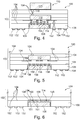
- Figure 1 illustrates a cross-sectional view of a component carrier 100 according to an exemplary embodiment of the invention.
- a laminate-type component carrier 100 is provided which is configured as a plate-shaped PCB (printed circuit board) or IC (integrated circuit) substrate.
- the component carrier 100 is configured as a transceiver having both transmitter and receiver capability.
- the component carrier 100 is configured for communicating via a mobile communication network, Bluetooth and/or WiFi.
- the component carrier 100 may also be configured for a high frequency application, such as 5G (or higher subsequent versions).
- the component carrier 100 comprises a laminated stack 102 comprising electrically conductive layer structures 104 and electrically insulating layer structures 106. Lamination may particularly denote the connection of the layer structures 104, 106 by the application of pressure and/or heat.
- the electrically insulating layer structures 106 may for instance comprise resin (such as epoxy resin), optionally comprising reinforcing particles such as glass fibers.
- the electrically insulating layer structures 106 may be made of prepreg. It is also possible that at least part of the material of the electrically insulating layer structures 106 is a high-frequency dielectric having a lower high-frequency loss than standard prepreg material of a stack of component carrier material (for instance RO3003TM material, as commercialized by the company Rogers Corporation). By taking this measure, the component carrier 100 may be rendered highly appropriate for high-frequency applications.
- the electrically conductive layer structures 104 may be patterned copper layers laminated with the electrically insulating layer structures 106 and/or may be plated copper structures.
- a front end chip 108 embodied as a semiconductor chip, is accommodated in a cavity 114 of the stack 102 and extends up to a lower main surface of the stack 102.
- the front end chip 108 is accommodated in cavity 114 of the stack 102 and extends up to the lower main surface so that an exposed main surface of the front end chip 108 is substantially in flush with or aligned with a lower main surface of the stack 102. This simplifies substitution of the front-end chip 108, for instance for a redesign of the component carrier 100 or for another high-frequency application.
- An antenna interface 110 is arranged on an opposing other (according to Figure 1 upper) main surface of the stack 102. More specifically, the component carrier 100 of Figure 1 comprises an antenna 116 connected to the antenna interface 110, i.e. antenna 116 is embodied as a surface mounted device. More specifically, the illustrated antenna 116 is here configured as a chip antenna.
- an impedance matching circuitry 112 is provided as part of the component carrier 100 and is embedded in a central portion of the stack 102.
- impedance matching circuitry 112 is realized by an IPD (integrated passive device).
- the impedance matching circuitry 112 is vertically sandwiched between the front end chip 108 and the antenna interface 110.
- the impedance matching circuitry 112 is configured for matching an impedance between the front end chip 108 and the antenna 116 connected to the antenna interface 110.
- the impedance matching circuitry 112 may be configured as a Balun.
- the impedance matching circuitry 112 is configured as an impedance matching semiconductor chip providing an impedance matching functionality when embedded as a whole in the stack 102.
- the Balun is here configured as a component which is embedded in the module-type component carrier 100.
- the antenna interface 110, the impedance matching circuitry 112 and the front end chip 108 are vertically stacked above each other and are advantageously electrically connected with each other substantially exclusively by vertical through connections 118 (compare Figure 1 ). This keeps the component carrier 100 compact and the signal paths short. This results, in turn, in low losses.
- Figure 1 shows a cross-sectional view of a PCB (printed circuit board) type laminated component carrier 100 being shaped as a plate.
- Impedance matching circuitry 112 is embedded in a central portion of the stack 102.
- cavity 114 is formed in which front end chip 108 is accommodated with exterior access from a bottom side of the component carrier 100.
- the cavity 114 may be formed for example by embedding in the stack 102 a poorly adhesive layer, for instance made of a waxy material or Teflon.
- a circumferential cut may be made from a lower main surface of the stack 102, for instance with a laser, to thereby cut out a piece of the stack 102 which is delimited circumferentially by the laser cutting line and horizontally by the poorly adhesive layer.
- cavity 114 is formed.
- the front end chip 108 may be inserted into the so formed cavity 114.
- the antenna 116 of Figure 1 is a surface-mounted device, for instance a ceramic antenna, on the stack 102.
- the impedance matching circuitry 112 Vertically in between the antenna 116 and the front end chip 108 is the impedance matching circuitry 112, which can be configured as a Balun component.
- substantially vertical through-connections 118 are formed as part of the electrically conductive layer structures 104 so as to connect constituents 108, 112 and 116 in the vertical direction so that a substantially vertical signal flow is enabled. This keeps the component carrier 100 compact and the signal quality high.
- electrically conductive pads 152 are formed on a lower main surface of the component carrier 100. By the pads 152, the component carrier 100 can be mounted and simultaneously electrically connected with a mounting base (see reference sign 124 in Figure 9 ) such as a printed circuit board.
- a wireless signal in form of electromagnetic radiation is captured by the antenna 116 and is conducted by the impedance matching circuitry 112 to the front end chip 108 for further processing.
- an electric signal is created by the front-end chip 108 and is transmitted by the impedance matching circuitry 112 to the antenna 116 for transmission in form of electromagnetic radiation.
- thermally conductive adhesives as an underfill material for the semiconductor chip.
- These adhesives may increase the adhesion between the chip and the PCB and may additionally enhance the thermal energy distribution.
- a thermal grease may be an underfill with enhanced thermal performance.
- Voids between the semiconductor chip and the cavity may be filled with an underfill material (thermally conductive adhesive) which may additionally exhibit a thermal conductivity of up to 10 W/mK, in particular up to 20 W/mK, or more. Thereby, the thermal energy distribution may be enhanced.
- Figure 2 illustrates a cross-sectional view of a component carrier 100 according to another exemplary embodiment of the invention.
- the antenna 116 is a loop antenna which may for instance be formed by patterned electrically conductive material of the electrically conductive layer structures 104. Such a configuration is particularly compact and simple in manufacture.
- a shielding structure 120 for shielding electromagnetic radiation between the impedance matching circuitry 112 and the front-end chip 108 on the one hand, and the antenna 116 on the other hand is provided. More specifically, the shielding structure 120 may be embodied as a substantially continuous magnetic layer or a substantially continuous electrically conductive layer.
- the antenna 116 which is embodied as patterned copper layer(s) on top of the stack 102 according to Figure 2
- a layer of a magnetic material is embedded in the stack 102 to thereby form magnetic shielding 120. Consequently, electromagnetic radiation is prevented from propagating between the antenna 116 and the front end chip 108, which improves the signal quality.
- the component carrier 100 of Figure 2 comprises a via-in-via 122 forming part of the vertical through-connections 118.
- a via-in-via 122 With such a via-in-via 122, a transmitted signal can be properly shielded with respect to an electronic environment.
- the vertical arrangement of the via-in-via 122 keeps the signal paths short and high-frequency losses small.
- Figure 2 illustrates that some of the vertical through-connections 118 of the electrically conductive layer structures 104 are configured as via-in-via 122.
- Such a via-in-via structure may function as a coax cable and may therefore further improve the shielding of signals propagating along the central electrically conductive core of the via-in-via 122.
- the impedance matching circuit 112 is not realized as a single embedded semiconductor component as in Figure 1 , but as a combination of one or more resistor components, one or more inductance components and/or one or more capacitor components cooperating with electric circuitry constituted by the electrically conductive layer structures 104 to thereby form impedance matching circuitry 112.
- the impedance matching circuitry 112 of Figure 2 is configured as an arrangement of circuit elements of the stack 102 and may be formed by the electrically conductive layer structures 104. Said plurality of capacitor elements, resistor elements, inductor elements, etc. may form part of the stack 102 and may be interconnected by the wiring of the PCB in such a way that an impedance matching function is achieved.
- the configuration according to Figure 2 can be used particularly advantageously for high frequency applications. It may be possible that there is no dedicated die or passive component installed.
- the copper structure itself may act as a balun between the antenna 116 and the front end chip 108.
- components 112a, 112b may be installed to stabilize the power supply for the front end chip 108.
- components 112a, 112b may exhibit a low-pass filter, a high-pass filter or a bandpass filter.
- a component carrier 100 according to another exemplary embodiment shown in Figure 3 differs from the component carrier 100 shown in Figure 2 in that, according to Figure 3 , the impedance matching circuitry 112 is here embodied as an embedded component. The latter is vertically sandwiched between the front end chip 108 and the antenna 116. The latter is again manufactured as a patterned electrically conductive layer structure 104 on top of the stack 102. Also in Figure 3 , the signal propagation paths are short due to the substantially vertical electric connection circuitry.
- the exemplary embodiment of the invention according to Figure 4 differs from the embodiment in Figure 3 in particular in that the antenna 116 is not embodied as a structured metal layer on top of the stack 102, but in contrast to this as an antenna component.
- Said antenna component may for instance be a ceramic component surface mounted on the stack 102 to provide an antenna function.
- Figure 5 shows only part of a component carrier 100 according to another exemplary embodiment of the invention illustrating that the cavity 114 accommodating the front end chip 108 can also be filled with an underfill material 158.
- the mechanical coupling of the front end chip 108 accommodated in the cavity 114 is thus further improved by providing the adhesive or underfill material 158. This may improve the thermal performance and the mechanical integrity of the component carrier 100 shown in Figure 5 .
- Figure 6 shows only part of a component carrier 100 according to an exemplary embodiment of the invention illustrating that the connection of the front end chip 108 within the stack 102 can also be accomplished by copper pillars 151.
- a schematically indicated impedance matching circuitry 112 can be formed by a corresponding configuration of the electrically conductive layer structures 104 of the stack 102.
- the copper circuitry (see reference signs 104, 116) may contribute to impedance matching.
- the antenna 116 is again formed as a patterned planar electrically conductive layer structure 104 on top of the stack 102, i.e. as an antenna structure. Therefore, the configuration of Figure 7 is particularly compact.
- the front end chip 108 is accommodated within a cavity 114 on the back side of the stack 102.
- connection structure 182 which may be configured for establishing a mechanical and an electrical connection to a mounting base 124 or carrier (see Figure 9 ).
- a connection may be a QFN (Quad Flat No Leads Package) connection, a BGA (Ball Grid Array) connection, etc.
- FIG 8 illustrates a circuitry of a Balun which may be implemented as impedance matching circuitry 112 in a component carrier 100 according to an exemplary embodiment of the invention.
- the impedance matching circuitry 112 is sandwiched between an antenna 116 and a front end chip 108.
- the Balun circuitry is composed of capacitors 160 and inductors 162 connected between the antenna 116 and the front end chip 108 and being partially grounded.
- impedance matching circuitry 112 may contribute to impedance matching.
- ohmic resistors not shown in Figure 8 may form part of impedance matching circuitry 112.
- Figure 9 illustrates a smart device 130 according to an exemplary embodiment of the invention.
- the illustrated smart device 130 may be a smartphone, a tablet, a phablet, a laptop, or a game console.
- the illustrated smart device 130 comprises a component carrier 100, for instance one of the component carriers 100 described above referring to Figure 1 to Figure 7 .
- the main surface of the component carrier 100 at which the front end chip 108 is exposed is mounted on a mounting base 124 of the smart device 130.
- the cross-sectional view of Figure 9 shows that the smart device 130 can be implemented in a very flat configuration.
- the flat component carrier 100 may be surface-mounted on the flat mounting base 124, such as a printed circuit board, within a casing 165 of the smart device 130.
- the component carrier 100 can provide its transceiver functionality with integrated front end processing and impedance matching capability even under very limited space conditions.
- FIG 10 illustrates a cross-sectional view of a component carrier 100 according to another exemplary embodiment of the invention.
- the antenna interface 110 is a socket 166 for connecting an antenna 116 via an electric cable 170.
- the socket 166 has an accommodation opening configured for receiving an inversely shaped plug 168 connected via coax cable 170 to the external antenna 116 embodied as antenna component 174.
- the external antenna component 174 may be a ceramic antenna.
- the front end chip 108 is surface-mounted on a lower main surface of the stack 102 to thereby protrude beyond a lower main surface of the stack 102. Also in this configuration, the front end chip 108 is properly accessible.
- Figure 11 illustrates a cross-sectional view of a component carrier 100 according to another exemplary embodiment of the invention.
- a side wall 123 of the stack 102 comprises an electrically conductive connection structure 126 configured for mounting and connecting the component carrier 100 on a mounting base 124 of a smart device 130, or on another electronic component or carrier.
- Figure 11 thus shows a configuration at which a side wall plating of the component carrier 100 is realized as electrically conductive connection structure 126.
- side wall 123 of the stack 102 is plated with electrically conductive material to thereby form the connection structure 126.
- FIG. 12 shows a smart device 130 according to an exemplary embodiment of the invention embodied as a smartphone.
- the smart device 130 may have a touchscreen 190, a control button 192, a camera 194, a loudspeaker 196 and a microphone 198, etc.
- a balun network can be also included in the front-end chip 108.
- the production and testing gets easier. Every part can be tested during the production cycle as the embedding (balun die) or the copper structure to balance.
- the antenna 116 can be tested before the front end chip 108 is installed in the component carrier 100. After installing the front end chip, the overall configuration is testable. Reference is made for instance of the embodiment of Figure 2 .
Landscapes
- Engineering & Computer Science (AREA)
- Microelectronics & Electronic Packaging (AREA)
- Computer Networks & Wireless Communication (AREA)
- Signal Processing (AREA)
- Manufacturing & Machinery (AREA)
- Production Of Multi-Layered Print Wiring Board (AREA)
- Details Of Aerials (AREA)
Priority Applications (3)
| Application Number | Priority Date | Filing Date | Title |
|---|---|---|---|
| EP19217655.0A EP3840542A1 (fr) | 2019-12-18 | 2019-12-18 | Support de composant stratifié compact avec puce d'extrémité avant et circuit d'adaptation d'impédance pour communication d'antenne |
| US17/247,394 US11394105B2 (en) | 2019-12-18 | 2020-12-09 | Compact laminated component carrier with front end chip and impedance matching circuitry for antenna communication |
| CN202011503076.8A CN113013134B (zh) | 2019-12-18 | 2020-12-17 | 部件承载件及其制造方法和使用方法及智能装置 |
Applications Claiming Priority (1)
| Application Number | Priority Date | Filing Date | Title |
|---|---|---|---|
| EP19217655.0A EP3840542A1 (fr) | 2019-12-18 | 2019-12-18 | Support de composant stratifié compact avec puce d'extrémité avant et circuit d'adaptation d'impédance pour communication d'antenne |
Publications (1)
| Publication Number | Publication Date |
|---|---|
| EP3840542A1 true EP3840542A1 (fr) | 2021-06-23 |
Family
ID=68965686
Family Applications (1)
| Application Number | Title | Priority Date | Filing Date |
|---|---|---|---|
| EP19217655.0A Pending EP3840542A1 (fr) | 2019-12-18 | 2019-12-18 | Support de composant stratifié compact avec puce d'extrémité avant et circuit d'adaptation d'impédance pour communication d'antenne |
Country Status (3)
| Country | Link |
|---|---|
| US (1) | US11394105B2 (fr) |
| EP (1) | EP3840542A1 (fr) |
| CN (1) | CN113013134B (fr) |
Cited By (1)
| Publication number | Priority date | Publication date | Assignee | Title |
|---|---|---|---|---|
| CN118076038A (zh) * | 2024-02-27 | 2024-05-24 | 江苏富乐华半导体科技股份有限公司 | 一种自动化生产的集中控制系统 |
Families Citing this family (12)
| Publication number | Priority date | Publication date | Assignee | Title |
|---|---|---|---|---|
| JP6962346B2 (ja) * | 2019-03-26 | 2021-11-05 | 株式会社Soken | アンテナ装置 |
| US12132509B2 (en) * | 2020-01-08 | 2024-10-29 | Skyworks Solutions, Inc. | Ultrahigh band architecture for radio frequency front-ends |
| US12610451B2 (en) * | 2020-04-27 | 2026-04-21 | At&S Austria Technologie & Systemtechnik Aktiengesellschaft | Component carrier with an embedded thermally conductive block and manufacturing method |
| DE102021109974A1 (de) * | 2020-04-27 | 2021-10-28 | At & S Austria Technologie & Systemtechnik Aktiengesellschaft | Bauteilträger mit einem eingebetteten wärmeleitfähigen Block und Herstellungsverfahren |
| US11735804B2 (en) * | 2020-05-11 | 2023-08-22 | Qualcomm Incorporated | Multi-core broadband PCB antenna |
| US20220368003A1 (en) * | 2021-05-14 | 2022-11-17 | Mediatek Inc. | Antenna module and manufacturing method thereof |
| CN113571872A (zh) * | 2021-07-27 | 2021-10-29 | 安徽安努奇科技有限公司 | 一种内匹配芯片天线及其制造方法 |
| CN113594153B (zh) * | 2021-07-30 | 2024-04-05 | 东莞记忆存储科技有限公司 | 一种存储芯片封装结构及其加工工艺方法 |
| CN114915330A (zh) * | 2022-03-31 | 2022-08-16 | 航天恒星科技有限公司 | 一种基带射频一体化的卫星终端 |
| CN116990760A (zh) * | 2023-08-02 | 2023-11-03 | 北京木牛领航科技有限公司 | 一种片上天线阻抗匹配方法和雷达系统 |
| US20250183237A1 (en) * | 2023-12-01 | 2025-06-05 | Taiwan Semiconductor Manufacturing Company Limited | Package structure including a backside metal film on a semiconductor die and a thermally conductive underfill layer on the backside metal film and methods of forming the same |
| CN121692525A (zh) * | 2026-02-11 | 2026-03-17 | 浙江大学 | 射频组件结构、其组装及维护方法 |
Citations (6)
| Publication number | Priority date | Publication date | Assignee | Title |
|---|---|---|---|---|
| EP1769430A1 (fr) * | 2004-06-18 | 2007-04-04 | Avery Dennison Corporation | Dispositif d'identification par radiofrequence (rfid) et procede de fabrication |
| US20120188138A1 (en) * | 2011-01-21 | 2012-07-26 | International Business Machines Corporation | Laminated antenna structures for package applications |
| US9935065B1 (en) * | 2016-12-21 | 2018-04-03 | Infineon Technologies Ag | Radio frequency device packages and methods of formation thereof |
| EP3547363A1 (fr) * | 2018-03-29 | 2019-10-02 | AT & S Austria Technologie & Systemtechnik Aktiengesellschaft | Ensemble électronique et système électronique avec des structures d'interconnexion à adaptation d'impédance |
| US20190304936A1 (en) * | 2018-04-02 | 2019-10-03 | Intel Corporation | Microelectronic assemblies having front end under embedded radio frequency die |
| EP3579334A1 (fr) * | 2018-06-06 | 2019-12-11 | AT & S Austria Technologie & Systemtechnik Aktiengesellschaft | Fonctionnalité rf et blindage de protection contre le rayonnement électromagnétique dans un support de composants |
Family Cites Families (13)
| Publication number | Priority date | Publication date | Assignee | Title |
|---|---|---|---|---|
| GB9117829D0 (en) * | 1991-08-15 | 1991-10-09 | Amulet Electronics Ltd | Impedance matching |
| US6876836B2 (en) * | 2002-07-25 | 2005-04-05 | Integrated Programmable Communications, Inc. | Layout of wireless communication circuit on a printed circuit board |
| DE102006007381A1 (de) | 2006-02-15 | 2007-08-23 | Infineon Technologies Ag | Halbleiterbauelement für einen Ultraweitband-Standard in der Ultrahochfrequenz-Kommunikation und Verfahren zur Herstellung desselben |
| KR100835061B1 (ko) | 2007-06-11 | 2008-06-03 | 삼성전기주식회사 | 반도체 칩 패키지 |
| US7859359B2 (en) | 2008-02-25 | 2010-12-28 | Broadcom Corporation | Method and system for a balun embedded in an integrated circuit package |
| US8217272B2 (en) | 2009-12-18 | 2012-07-10 | Intel Corporation | Apparatus and method for embedding components in small-form-factor, system-on-packages |
| US8218323B2 (en) | 2009-12-18 | 2012-07-10 | Intel Corporation | Apparatus and method for embedding components in small-form-factor, system-on-packages |
| JP5664829B2 (ja) | 2012-11-29 | 2015-02-04 | 株式会社村田製作所 | 高周波モジュール |
| US10515924B2 (en) * | 2017-03-10 | 2019-12-24 | Skyworks Solutions, Inc. | Radio frequency modules |
| US10410963B1 (en) * | 2018-06-07 | 2019-09-10 | At&S Austria Technologie & Systemtechnik Aktiengesellschaft | Deformed layer for short electric connection between structures of electric device |
| EP3633721A1 (fr) * | 2018-10-04 | 2020-04-08 | AT & S Austria Technologie & Systemtechnik Aktiengesellschaft | Support de composants comportant des composants intégrés face vers le haut et face vers le bas |
| US10888002B2 (en) * | 2019-03-28 | 2021-01-05 | At&S Austria Technologie & Systemtechnik Aktiengesellschaft | Component carrier with embedded tracks protruding up to different heights |
| KR102609138B1 (ko) * | 2019-04-29 | 2023-12-05 | 삼성전기주식회사 | 인쇄회로기판 어셈블리 |
-
2019
- 2019-12-18 EP EP19217655.0A patent/EP3840542A1/fr active Pending
-
2020
- 2020-12-09 US US17/247,394 patent/US11394105B2/en active Active
- 2020-12-17 CN CN202011503076.8A patent/CN113013134B/zh active Active
Patent Citations (7)
| Publication number | Priority date | Publication date | Assignee | Title |
|---|---|---|---|---|
| EP1769430A1 (fr) * | 2004-06-18 | 2007-04-04 | Avery Dennison Corporation | Dispositif d'identification par radiofrequence (rfid) et procede de fabrication |
| EP1769430B1 (fr) * | 2004-06-18 | 2008-09-24 | Avery Dennison Corporation | Dispositif d'identification par radiofrequence (rfid) et procede de fabrication |
| US20120188138A1 (en) * | 2011-01-21 | 2012-07-26 | International Business Machines Corporation | Laminated antenna structures for package applications |
| US9935065B1 (en) * | 2016-12-21 | 2018-04-03 | Infineon Technologies Ag | Radio frequency device packages and methods of formation thereof |
| EP3547363A1 (fr) * | 2018-03-29 | 2019-10-02 | AT & S Austria Technologie & Systemtechnik Aktiengesellschaft | Ensemble électronique et système électronique avec des structures d'interconnexion à adaptation d'impédance |
| US20190304936A1 (en) * | 2018-04-02 | 2019-10-03 | Intel Corporation | Microelectronic assemblies having front end under embedded radio frequency die |
| EP3579334A1 (fr) * | 2018-06-06 | 2019-12-11 | AT & S Austria Technologie & Systemtechnik Aktiengesellschaft | Fonctionnalité rf et blindage de protection contre le rayonnement électromagnétique dans un support de composants |
Cited By (1)
| Publication number | Priority date | Publication date | Assignee | Title |
|---|---|---|---|---|
| CN118076038A (zh) * | 2024-02-27 | 2024-05-24 | 江苏富乐华半导体科技股份有限公司 | 一种自动化生产的集中控制系统 |
Also Published As
| Publication number | Publication date |
|---|---|
| CN113013134A (zh) | 2021-06-22 |
| US11394105B2 (en) | 2022-07-19 |
| CN113013134B (zh) | 2024-04-26 |
| US20210194111A1 (en) | 2021-06-24 |
Similar Documents
| Publication | Publication Date | Title |
|---|---|---|
| US11394105B2 (en) | Compact laminated component carrier with front end chip and impedance matching circuitry for antenna communication | |
| CN110572926B (zh) | 部件承载件中的rf功能和电磁辐射屏蔽 | |
| US11121476B2 (en) | Chip antenna module | |
| US7808434B2 (en) | Systems and methods for integrated antennae structures in multilayer organic-based printed circuit devices | |
| EP1387369A1 (fr) | Dispositif a module haute frequence | |
| EP3547363A1 (fr) | Ensemble électronique et système électronique avec des structures d'interconnexion à adaptation d'impédance | |
| WO2019020795A1 (fr) | Structure d'antenne sur diélectrique haute fréquence dans une cavité d'un support de composant | |
| US20250040028A1 (en) | Rf front-end functionality integrated in a component carrier stack | |
| US20220299595A1 (en) | Component Carrier with Embedded High-Frequency Component and Integrated Waveguide for Wireless Communication | |
| US11322482B2 (en) | Component carrier with opposed stacks having respective connection bodies and a method for manufacturing the component carrier | |
| US11140768B2 (en) | Component carrier with high passive intermodulation performance | |
| US12279369B2 (en) | Electrically connected component carrier stacks with respective cavities and method of manufacturing the same | |
| EP4312470A1 (fr) | Support de composant avec élément conducteur de signal et structure conductrice de blindage | |
| US20260040432A1 (en) | Component carrier with signal conductive element and shielding conductive structure | |
| US20250364713A1 (en) | Dielectric Element in Component Carrier Embedded Waveguide | |
| US20250087891A1 (en) | Component Carrier with Protruding Dielectric Signal Element and Manufacture Method |
Legal Events
| Date | Code | Title | Description |
|---|---|---|---|
| PUAI | Public reference made under article 153(3) epc to a published international application that has entered the european phase |
Free format text: ORIGINAL CODE: 0009012 |
|
| STAA | Information on the status of an ep patent application or granted ep patent |
Free format text: STATUS: THE APPLICATION HAS BEEN PUBLISHED |
|
| AK | Designated contracting states |
Kind code of ref document: A1 Designated state(s): AL AT BE BG CH CY CZ DE DK EE ES FI FR GB GR HR HU IE IS IT LI LT LU LV MC MK MT NL NO PL PT RO RS SE SI SK SM TR |
|
| STAA | Information on the status of an ep patent application or granted ep patent |
Free format text: STATUS: REQUEST FOR EXAMINATION WAS MADE |
|
| 17P | Request for examination filed |
Effective date: 20211222 |
|
| RBV | Designated contracting states (corrected) |
Designated state(s): AL AT BE BG CH CY CZ DE DK EE ES FI FR GB GR HR HU IE IS IT LI LT LU LV MC MK MT NL NO PL PT RO RS SE SI SK SM TR |
|
| STAA | Information on the status of an ep patent application or granted ep patent |
Free format text: STATUS: EXAMINATION IS IN PROGRESS |
|
| 17Q | First examination report despatched |
Effective date: 20230112 |