EP3842823B1 - Mikrowellenempfänger - Google Patents
Mikrowellenempfänger Download PDFInfo
- Publication number
- EP3842823B1 EP3842823B1 EP20210613.4A EP20210613A EP3842823B1 EP 3842823 B1 EP3842823 B1 EP 3842823B1 EP 20210613 A EP20210613 A EP 20210613A EP 3842823 B1 EP3842823 B1 EP 3842823B1
- Authority
- EP
- European Patent Office
- Prior art keywords
- state
- receiver
- microwave signal
- electronically controllable
- controllable switch
- Prior art date
- Legal status (The legal status is an assumption and is not a legal conclusion. Google has not performed a legal analysis and makes no representation as to the accuracy of the status listed.)
- Active
Links
Images
Classifications
-
- G—PHYSICS
- G01—MEASURING; TESTING
- G01S—RADIO DIRECTION-FINDING; RADIO NAVIGATION; DETERMINING DISTANCE OR VELOCITY BY USE OF RADIO WAVES; LOCATING OR PRESENCE-DETECTING BY USE OF THE REFLECTION OR RERADIATION OF RADIO WAVES; ANALOGOUS ARRANGEMENTS USING OTHER WAVES
- G01S7/00—Details of systems according to groups G01S13/00, G01S15/00, G01S17/00
- G01S7/02—Details of systems according to groups G01S13/00, G01S15/00, G01S17/00 of systems according to group G01S13/00
- G01S7/03—Details of HF subsystems specially adapted therefor, e.g. common to transmitter and receiver
- G01S7/034—Duplexers
-
- G—PHYSICS
- G01—MEASURING; TESTING
- G01S—RADIO DIRECTION-FINDING; RADIO NAVIGATION; DETERMINING DISTANCE OR VELOCITY BY USE OF RADIO WAVES; LOCATING OR PRESENCE-DETECTING BY USE OF THE REFLECTION OR RERADIATION OF RADIO WAVES; ANALOGOUS ARRANGEMENTS USING OTHER WAVES
- G01S7/00—Details of systems according to groups G01S13/00, G01S15/00, G01S17/00
- G01S7/02—Details of systems according to groups G01S13/00, G01S15/00, G01S17/00 of systems according to group G01S13/00
- G01S7/28—Details of pulse systems
- G01S7/285—Receivers
Definitions
- the present invention relates to a microwave signal receiver. It is applied, for example, in radar systems to protect the receiver components from high power incident signals.
- Some microwave signal receivers are known to use power limiters to protect the receiver components from relatively high power incident signals. This happens, for example, in radar system receivers in which the delicate and sensitive components of the receiver must be protected from direct returns from the radar transmitter. Excessively high power signals can impair both the proper functioning of the receiver components and cause irreversible damage to them.
- waveguide power limiters are known to be used to protect the receiver components from high power incident signals.
- a microwave waveguide power limiter is described in the article " Investigation and design of microwave waveguide power limiter for communications and radar applications", by Yasser M. Madany and Ahmed F. Miligy, 2015 International Conference on Electromagnetics in Advanced Applications (ICEAA) - IEEE .
- the waveguide power limiters have some drawbacks. Indeed, the waveguide power limiters in some applications, e.g. in radar integrated into missile seekers, have a relatively large footprint and weight. Furthermore, the integration and testing operations of a radar system receiver are particularly complex when the receiver has a waveguide limiter operationally connected to a subsequent circuit section of the receiver made as a microstrip, for example. Indeed, separate testing activities are initially required for the waveguide section and the microstrip section of the receiver. After assembly, the entire receiver must be tested both individually and after integration into the radar system.
- a microwave signal receiver comprising a waveguide power limiter is bulky, expensive, heavy.
- Document JP 2013 090263 A describes embodiments of a radar receiver in which the use of a limiter is provided before an SPST (Single Pole Single Throw) switch with an internal resistor or an SPDT (Single Pole Double Throw) switch with an external bypass resistor.
- an LNA amplifier is placed immediately downstream of the SPDT or SPDT switch. Due to the presence of the limiter, the aforesaid receiver has relatively long response times because the recovery time of the limiter from saturation state to the linearity state is typically 75ns-100ns.
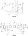
- Figure 1 shows a non-exhaustive, non-limiting embodiment of a radar system 1, comprising a transmitter 2 adapted to emit a radar signal s_tx and a microwave signal receiver 10 adapted to receive a radar return signal s_rx.
- the radar 1 is, for example, intended to be used aboard a missile or rocket and is integrated into the seeker of the missile or rocket.
- the radar system 1 further comprises a transmitter antenna 3 operationally connected to the transmitter 2 for remote and radio transmission of the signal produced by the transmitter 2.
- the transmitting antenna 3 comprises e.g. one or more arrays of radiant antenna elements, e.g. one or more arrays of slot radiant elements.
- the assembly comprising the transmitter 2 and the transmitter antenna 3 is the transmission front end of the radar system 1.
- the radar 1 further comprises a local oscillator 4 adapted to synthesize and provide an oscillator signal s_ol sent in input to both the transmitter 2 and the microwave signal receiver 10.
- the transmitter 2 comprises a phase modulator, e.g. adapted to modulate the oscillator signal s_ol with a phase code so that it provides in output a signal having a coded pulse sequence which is fed to transmitter antenna 3.
- the transmitter 2 may comprise one or more amplifiers.
- the microwave radio signal output from the transmitting antenna s_tx represents the transmitted radar signal s_tx.
- the transmitted radar signal s_tx is a signal with a phase coded pulse sequence.
- the received signal s_rx also called radar return signal, includes a possible useful signal component, i.e. the signal reflected by a possible T target, and a disturbance signal component, essentially represented by undesired reflections on the ground, water, vegetation or infrastructure and direct returns.
- the aforesaid radar return signal s_rx further comprises a component due to a direct return in the receiver 10 of the signal s_tx transmitted by the transmitting antenna 3.
- the radar system 1 comprises a radio frequency reception front end 9,10 for receiving the radar return signal s_rx, adapted to process the radar return signal received to produce an output signal which is preferably an intermediate frequency signal s_if.
- the radio frequency reception front end 9,10 comprises a receiver antenna 9 for receiving the radar return signal s_rx.
- the receiving antenna 9 comprises one or more arrays of slot antennas.
- the output signal from the antenna 9 was also named return signal s_rx.
- a radar 1 system comprising a dedicated antenna 3 for transmission and a dedicated reception antenna 9 has been described so far, it is apparent to a person skilled in the art that, e.g. by means of a circulator, the same antenna 3 or antenna system used in transmission can be used for the reception of the radar return signal s_rx.
- the radar system 1 also comprises a radar processor 5 operationally connected to both the transmitter 2 and the microwave signal receiver 10.
- the radar processor 5 is a hardware and software system, comprising at least one processing unit, such as a general purpose or dedicated processor or an FPGA or DSP.
- the radar system 1 preferably comprises a frequency conversion module 6 to produce a baseband signal s_bb from the intermediate frequency signal s_if. Furthermore, the radar system 1 preferably comprises an analog to digital converter 7 to convert the baseband s_bb signal produced at the receiver 10 output into a digital sample stream s_d.
- the analog to digital converter 10 is operationally connected to radar processor 5 to provide the latter with the digital sample stream s_d. According to an alternative embodiment, the analog to digital converter 7 could be integrated into the receiver 10 or the radar processor 5.
- the radar processor 5 is configured to control the transmitter 2 and the receiver 10 and is preferably also programmed to receive and process the digital sample stream s_d to extract information regarding the presence and/or features of a target T.
- the receiver 10 is represented as a single channel receiver in the functional block chart in figure 2 .
- the receiver 10 may have a higher number of channels, mutually in parallel, replicating the diagram in figure 2 .
- radar system 1 is a monopulse radar system
- the receiver 10 could have four parallel channels to process four signals from four respective portions of receiver antenna 9.
- the microwave signal receiver 10 is such to provide an L-band microwave signal as output.
- the signal s_tx provided in output from the transmission front-end 2, 3 is a Ka-band signal, instead. The same goes for the radar return signal s_rx.
- receiver 10 is described in this document as being part of the radar system 1, the teachings of the present description are not limited to this type of receiver 10 and extend to microwave signal receivers not belonging to a radar system, e.g. data telecommunication receivers.
- the microwave signal receiver 10 comprises a printed circuit board 11, in particular a microstrip circuit board, comprising an input port 12 adapted to be operatively connected to an antenna 9, and in the example to the receiving antenna 9 of the radar system 1, to receive in input a microwave signal picked up by the antenna 9, which in this example is the radar return signal s rx.
- the output signal from the antenna 9 of the receiving front end 9,10 propagates within a waveguide, e.g. a WR28 waveguide, and the receiver 10 further comprises a guide-to-microstrip transition.
- a waveguide e.g. a WR28 waveguide
- the receiver 10 further comprises at least one power dissipator R1 and at least one electronically controllable switch 13 adapted to receive in input the microwave signal s_rx and a first control signal s_blk.
- the first control signal s_blk is a blanking signal, e.g. supplied to receiver 10 by the radar processor 5.
- a blanking signal in a radar system makes it possible to mutually synchronize the operation of the transmitter 2 and the receiver 10.
- the receiver 10 is devoid of a limiter, or any limiter, upstream of the electronically controllable switch 13. In other words, the microwave signal s_rx received at the input of the electronically controllable switch 13 does not pass through any limiter before it is received by the electronically controllable switch 13.
- the power dissipator R1 is a termination dissipator (as clearly shown in the diagram in figure 2 ) and the electronically controllable switch 13 comprises a first output port p1 and the electronically controllable switch 13 is configured to assume according to the control signal s_blk:
- the receiver 10 is integrated into a radar system 1, it is thus apparent that when the electronically controllable switch 13 is in the conduction state, the radar 1 system is in the receiving configuration and when the electronically controllable switch 13 is in the protection state the radar 1 system is in the transmitting configuration.
- the microwave signal receiver 10 further comprises at least one low-noise amplifier 15, i.e. an LNA (Low-Noise Amplifier), comprising an input port operationally connected to the first output port p1 of the electronically controllable switch 13 to receive the microwave signal s_rx in input and further comprising an output port to provide an amplified microwave signal s_a in output.
- LNA Low-Noise Amplifier
- the electronically controllable switch 13 is a PIN diode semiconductor switch. In this manner, a high switching speed of the electronically controllable switch 13 between the protection state and the conduction state and vice versa can be guaranteed.
- the rise and fall times of the electronically controllable switch 13 are less than 10 ns.
- the electronically controllable switch 13 has a high power handling, e.g. above 12W, e.g. equal to 13W.
- the electronically controllable switch 13 when in the protection state, guarantees insulation between the input and the first output port p1 of more than 35dB, e.g. either equal to about, or higher than, 40dB.
- the power dissipator R1 comprises a resistor external to the electronically controllable switch 13, preferably a resistor which allows high power to be dissipated in a small volume.
- a resistor is an aluminum nitride resistor and is preferably capable of dissipating at least 30W, preferably at least or approximately 40W, in Ka-band at a temperature of 50°C.
- the electronically controllable switch 13 is an SPDT - Single Pole Double Throw Switch - having a second output port p2 operationally connected to the power dissipator R1.
- the electronically controllable switch 13 is configured to make the microwave signal s_rx available to the second output port p2 so that the microwave signal s_rx can be routed to the dissipator R1.
- the low-noise amplifier 15 is adapted to assume an on and off state and is configured to assume:
- the low-noise amplifier 15 is also adapted and configured to receive the aforesaid first control signal s_blk, or in any event, a control signal correlated to it and is configured to assume the on state or off state based on the first control signal s_blk.
- the first control signal s_blk can be a blanking signal.
- the microwave signal receiver 10 also comprises an electronically controllable attenuator 14 operationally interposed between the electronically controllable switch 13 and the low-noise amplifier 15 to attenuate the microwave signal s_rx.
- the microwave signal receiver 10 is configured to control the electronically controllable attenuator 14 so that it assumes a first state in which the attenuator 14 has a relatively high attenuation and a second state in which attenuator 14 has relatively low attenuation, and in which the electronically controllable attenuator 14 assumes the first state when the electronically controllable switch 13 assumes the protection state.
- the electronically controllable attenuator 14 is adapted and configured to receive the aforesaid first control signal s_blk, or in any event, a control signal correlated to it and is configured to assume the relatively high attenuation state or the relatively low attenuation state based on the first control signal s_blk.
- the first control signal can be a blanking signal.
- the electronically controllable attenuator 14 in the relatively high attenuation state has an attenuation greater than 30dB, e.g. equal to 40dB, or about 40dB.
- the attenuator 14 is controlled to provide its maximum attenuation.
- the attenuator 14 is controlled to minimize its insertion loss.
- the electronically controllable attenuator 14 is a voltage controllable variable attenuator.
- the receiver 10 is the receiver of a radar system 1, during the transmission of the signal s_tx by the transmission front-end 2,3, the receiver 10 can be controlled by the first control signal s_blk, which is, for example, a blanking signal, to bring the electronically controllable switch 13 to the protection state, the electronically controllable attenuator 14 to the relatively high attenuation state and the low-noise amplifier 15 to off state at the same time.
- s_blk is, for example, a blanking signal
- the receiver 10 comprises a saturation estimate module 23, D1 of the receiver 10 adapted to detect whether the receiver 10 is in a saturation state or a linearity state.
- the receiver 10 is configured to control the electronically controllable attenuator 14 so that it assumes a third state in which it has an intermediate attenuation between the relatively high attenuation and the relatively low attenuation, e.g. equal to about 10dB.
- the receiver 10 When the electronically controllable switch 13 is in the conduction state, the receiver 10 is configured to control the electronically controllable attenuator 14 so that it assumes the second state if the receiver 10 is in the saturation state. Instead, when the electronically controllable switch 13 is in the conduction state, the receiver 10 is configured to control the electronically controllable attenuator 14 so that it assumes the third state if the receiver 10 is in the saturation state.
- the saturation estimation module 23, D1 is such to detect a saturating signal to supply a second control signal s_sat to the electronically controllable attenuator 14. Therefore, according to a particularly advantageous embodiment, the electronically controllable attenuator 14 is adapted and configured to receive both the first control signal s_blk and the second control signal s_sat, e.g. with an input port which produces the OR logic function between such control signals. Clearly, from a practical point of view, it is also possible for the electronically controllable attenuator 14 to receive a single control signal obtained from the first control signal s_blk and the second control signal s_sat by means of an appropriate logic.
- the saturation estimation block 23, D1 comprises a coupler 23 adapted and configured to tap a part of the received signal from the reception chain. It is possible to estimate the strength of such a tapped signal to detect whether the receiver 10 is in linearity or saturation.
- the saturation estimation block 23, D1 comprises a detector diode D1 which provides a voltage output s_v starting from the tapped signal. By comparing this voltage s_v with a threshold voltage Vth it is possible to produce the second s_sat control signal as a binary signal, which assumes a first value when the voltage s_v is higher than the threshold voltage and a second value otherwise. It is, therefore, possible to establish that the receiver 10 is in a linearity condition when the second control signal s_sat assumes the first value and the receiver 10 is in a linearity condition when the second control signal s_sat assumes the second value.
- the receiver 10 further comprises a further electronically controllable attenuator 16 which is arranged downstream of the low-noise amplifier 15.
- this additional attenuator 16 is only controlled based on the second control signal s_sat to manage the dynamics of the receiver 10 more flexibly and to ensure that the receiver works in linearity conditions when the electrically controllable switch 13 is in the conduction state.
- the receiver 10 further comprises an additional low-noise amplifier 17 and a fixed attenuator 18 downstream of the low-noise amplifier 15, in particular downstream of the additional attenuator 16.
- the latter is intended to achieve a tuning gain of the receiver 10.
- the receiver 10 comprises downstream of the low-noise amplifier 15, in the example in figure 2 downstream of the fixed attenuator 18, a band-pass filter 19 for image signal rejection, preferably followed by an additional fixed attenuator 20.
- the receiver 10 further comprises a frequency converter 21, such as a mixer, having an input port operationally connected to the output port of the low-noise amplifier 15 to convert the amplified microwave signal s_a, and in the example also attenuated and filtered, into an intermediate frequency signal s_if.
- a frequency converter 21 such as a mixer
- the saturation estimation module 23, D1 is such to detect whether the receiver 10 is in a saturation state or a linearity state starting from an amplitude or signal power measurement at intermediate frequency s_if. This is in accordance with the example shown in figure 2 , where the saturation estimation module 23, D1, the operation of which is shown above, is located downstream of the frequency converter 21.
- the frequency converter 21 is fed with the oscillator signal s_ol supplied by a local oscillator 4 and the receiver 10 comprises a bandpass filter 25 operationally interposed between the frequency converter 21 and the local oscillator 4 to filter the oscillator signal s_ol before supplying in input to the frequency converter 21.
- This device advantageously reduces the spurious components caused by the s_ol oscillator signal generated by local oscillator 4.
- receiver 10 comprises an amplifier 26 which then acts as a driver for frequency converter 21.
- spurious components are particularly harmful to receiver 10 because they can generate residues at the intermediate frequency Fif of the receiver 10 and thus in case of weak signals such spurious components may overlap the useful signal masking it and thus reducing the sensitivity of the receiver 10.
- the band-pass filter 25 e.g. made as a microstrip, is preferably centered at the frequency Fol.
- a bandpass filter 25 is adapted and configured to attenuate the spurious components present at the frequencies Frf ⁇ Fif by more than 15 dB and spurious components present at the frequency Fif by about 80 dB.
- the receiver 10 further comprises an intermediate frequency amplifier 22 and a step attenuator 24 downstream of the frequency converter 21 to allow further adjustment of the reception chain gain.
Landscapes
- Engineering & Computer Science (AREA)
- Computer Networks & Wireless Communication (AREA)
- Physics & Mathematics (AREA)
- General Physics & Mathematics (AREA)
- Radar, Positioning & Navigation (AREA)
- Remote Sensing (AREA)
- Input Circuits Of Receivers And Coupling Of Receivers And Audio Equipment (AREA)
- Radar Systems Or Details Thereof (AREA)
Claims (14)
- Mikrowellenempfänger (10), der eine gedruckte Leiterplatte (11), insbesondere eine Mikrostreifenleiterplatte, umfasst, die einen Eingangsanschluss umfasst, der dazu ausgebildet ist, operativ mit einer Antenne (9) verbunden zu werden, um am Eingang ein von der Antenne (9) aufgefangenes Mikrowellensignal (s_rx) zu empfangen, wobei der Mikrowellenempfänger (10) umfasst:- mindestens einen Leistungsableiter (R1);- einen elektronisch steuerbaren Schalter (13), der dazu ausgebildet ist, am Eingang das Mikrowellensignal (s_rx) und ein erstes Steuersignal (s_blk) zu empfangen, wobei der elektronisch steuerbare Schalter (13) einen ersten Ausgangsanschluss (p1) umfasst und wobei der elektronisch steuerbare Schalter (13) dazu konfiguriert ist, auf Grundlage des Steuersignals einen Leitungszustand, um das Mikrowellensignal (s_rx) an den ersten Ausgangsanschluss (p1) zu liefern, und einen Schutzzustand einzunehmen, in dem der elektronisch steuerbare Schalter (13) derart ist, dass er das Mikrowellensignal (s_rx) an den Leistungsableiter(R1) sendet;- mindestens einen Verstärker (15) mit niedriger Rauschzahl, der einen Eingangsanschluss umfasst, der operativ mit dem ersten Ausgangsanschluss (p1) verbunden ist, und der ferner einen Ausgangsanschluss zum Liefern eines verstärkten Mikrowellensignals (s_a) am Ausgang umfasst;wobei:- der elektronisch steuerbare Schalter (13) ein SPDT(Single Pole Double Throw)-Schalter ist, der einen zweiten Ausgangsanschluss (p2) aufweist, der betriebsmäßig mit dem Leistungsableiter (R1) verbunden ist, und wobei der elektronisch steuerbare Schalter (13) im Schutzzustand dazu konfiguriert ist, das Mikrowellensignal (s_rx) dem zweiten Ausgangsanschluss (p2) zur Verfügung zu stellen;- der Leistungsableiter (R1) ein Abschlussableiter ist;dadurch gekennzeichnet, dass der Mikrowellenempfänger (10) ferner ein elektronisch steuerbares Dämpfungsglied (14) umfasst, das operativ zwischen dem elektronisch steuerbaren Schalter (13) und dem Verstärker (15) mit niedriger Rauschzahl zum Dämpfen des Mikrowellensignals (s_rx) angeordnet ist, und wobei der Empfänger (10) dazu konfiguriert ist,das Dämpfungsglied (14) so zu steuern, dass Letzteres einen ersten Zustand, in dem es eine relativ hohe Dämpfung aufweist, und einen zweiten Zustand einnimmt, in dem es eine relativ geringe Dämpfung aufweist, und wobei das elektronisch steuerbare Dämpfungsglied (14) den ersten Zustand einnimmt, wenn der elektronisch steuerbare Schalter (13) den Schutzzustand einnimmt.
- Mikrowellenempfänger (10) nach Anspruch 1, wobei der elektronisch steuerbare Schalter (13) ein PIN-Dioden-Halbleiterschalter ist.
- Mikrowellenempfänger (10) nach Anspruch 1 oder 2, wobei der mindestens eine Leistungsableiter (R1) einen Widerstand außerhalb des elektronisch steuerbaren Schalters (13) umfasst, vorzugsweise einen Widerstand, der das Umwandeln hoher Leistung in ein kleines Volumen ermöglicht.
- Mikrowellenempfänger (10) nach Anspruch 3, wobei der Widerstand ein Aluminiumnitridwiderstand ist.
- Mikrowellenempfänger (10) nach einem der vorhergehenden Ansprüche, wobei der Empfänger (10) keinen dem elektronisch steuerbaren Schalter (13) vorgelagerten Begrenzer aufweist.
- Mikrowellenempfänger (10) nach einem der vorhergehenden Ansprüche, wobei der Verstärker (15) mit niedriger Rauschzahl dazu ausgebildet ist, einen Ein-Zustand und einen Aus-Zustand einzunehmen, und wobei der Verstärker mit niedriger Rauschzahl dazu konfiguriert ist, den Ein-Zustand einzunehmen, wenn sich der elektronisch steuerbare Schalter (13) im Leitungszustand befindet, und den Aus-Zustand einzunehmen, wenn sich der elektronisch steuerbare Schalter (13) im Schutzzustand befindet.
- Mikrowellenempfänger (10) nach Anspruch 6, wobei der Verstärker (15) dazu ausgebildet ist, das erste Steuersignal (s_blk) zu empfangen, und dazu konfiguriert ist, auf Grundlage des ersten Steuersignals (s_blk) den Ein-Zustand oder den Aus-Zustand einzunehmen.
- Mikrowellenempfänger (10) nach Anspruch 1, wobei:- der Empfänger (10) ein Sättigungsschätzmodul (23, D1) des Empfängers (10) umfasst, das dazu ausgebildet ist, zu erkennen, ob sich der Empfänger (10) in einem Sättigungszustand oder einem Linearitätszustand befindet,- der Empfänger (10) dazu konfiguriert ist, das elektronisch steuerbare Dämpfungsglied (13) so zu steuern, dass es einen dritten Zustand einnimmt, in dem es eine Zwischendämpfung zwischen der relativ hohen Dämpfung und der relativ niedrigen Dämpfung aufweist;- wenn sich der elektronisch steuerbare Schalter (13) im Leitungszustand befindet, der Empfänger (10) dazu konfiguriert ist, das elektronisch steuerbare Dämpfungsglied (14) so zu steuern, dass es den zweiten Zustand einnimmt, wenn sich der Empfänger (10) im Linearitätszustand befindet, und dass es den dritten Zustand einnimmt, wenn sich der Empfänger (10) im Sättigungszustand befindet.
- Mikrowellenempfänger (10) nach Anspruch 1, wobei das elektronisch steuerbare Dämpfungsglied (14) ein spannungssteuerbares variables Dämpfungsglied ist.
- Mikrowellenempfänger (10) nach Anspruch 1, der ein weiteres elektronisch steuerbares Dämpfungsglied (16) umfasst, das dem rauscharmen Verstärker (15) nachgelagert angeordnet ist.
- Mikrowellenempfänger (10) nach einem der vorhergehenden Ansprüche, der ferner einen Frequenzumwandler (21) umfasst, der einen Eingangsanschluss aufweist, der operativ mit dem Ausgangsanschluss des Verstärkers (15) mit niedriger Rauschzahl verbunden ist, um das verstärkte Mikrowellensignal (s_a) in ein Zwischenfrequenzsignal (s_if) umzuwandeln.
- Mikrowellenempfänger (10) nach den Ansprüchen 8 und 11, wobei das Sättigungsschätzmodul (23, D1) derart beschaffen ist, dass es ausgehend von einer Amplituden- oder Leistungsstärkemessung des Zwischenfrequenzsignals (s_if) erkennt, ob sich der Empfänger (10) in einem Sättigungszustand oder einem Linearitätszustand befindet.
- Mikrowellenempfänger (10) nach Anspruch 11 oder 12, wobei der Frequenzumsetzer mit einem von einem lokalen Oszillator (4) gelieferten Oszillatorsignal (s_ol) gespeist wird und wobei der Empfänger (10) ein Bandpassfilter (25) umfasst, das betriebsmäßig zwischen dem Frequenzumsetzer (21) und dem lokalen Oszillator (4) angeordnet ist, um das Oszillatorsignal (s_ol) zu filtern, bevor es dem Frequenzumsetzer (21) am Eingang geliefert wird.
- Radarsystem (1), das einen Mikrowellenempfänger (10) nach einem der vorhergehenden Ansprüche und einen Sender (2) umfasst, wobei das Radarsystem (1) dazu ausgebildet und konfiguriert ist, selektiv zwischen einem Sendebetriebszustand und einem Empfangsbetriebszustand umzuschalten, und wobei:- der elektronisch steuerbare Schalter (13) den Schutzzustand einnimmt, wenn sich das Radarsystem (1) im Sendebetriebszustand befindet,- der elektronisch steuerbare Schalter (13) den Leitungszustand einnimmt, wenn sich das Radarsystem (1) im Empfangsbetriebszustand befindet.
Applications Claiming Priority (1)
| Application Number | Priority Date | Filing Date | Title |
|---|---|---|---|
| IT102019000025285A IT201900025285A1 (it) | 2019-12-23 | 2019-12-23 | Ricevitore di segnali a microonde |
Publications (3)
| Publication Number | Publication Date |
|---|---|
| EP3842823A1 EP3842823A1 (de) | 2021-06-30 |
| EP3842823C0 EP3842823C0 (de) | 2024-11-06 |
| EP3842823B1 true EP3842823B1 (de) | 2024-11-06 |
Family
ID=70228553
Family Applications (1)
| Application Number | Title | Priority Date | Filing Date |
|---|---|---|---|
| EP20210613.4A Active EP3842823B1 (de) | 2019-12-23 | 2020-11-30 | Mikrowellenempfänger |
Country Status (3)
| Country | Link |
|---|---|
| EP (1) | EP3842823B1 (de) |
| ES (1) | ES2999366T3 (de) |
| IT (1) | IT201900025285A1 (de) |
Families Citing this family (2)
| Publication number | Priority date | Publication date | Assignee | Title |
|---|---|---|---|---|
| CN114779179A (zh) * | 2022-06-20 | 2022-07-22 | 成都远望探测技术有限公司 | 一种基于气象雷达的抗饱和接收电路 |
| CN116846413B (zh) * | 2023-07-18 | 2024-06-21 | 成都中微达信科技有限公司 | 一种基于复合通道的微波接收系统 |
Family Cites Families (4)
| Publication number | Priority date | Publication date | Assignee | Title |
|---|---|---|---|---|
| ATE451627T1 (de) * | 2002-03-22 | 2009-12-15 | Ericsson Telefon Ab L M | Sende-empfangs-schalter mit hochleistungsschutz |
| US6707417B2 (en) * | 2002-06-11 | 2004-03-16 | Raytheon Company | Accurate range calibration architecture |
| JP5235031B2 (ja) * | 2011-03-15 | 2013-07-10 | 島田理化工業株式会社 | リミッタ装置、レーダシステム |
| JP2013090263A (ja) * | 2011-10-21 | 2013-05-13 | Toshiba Corp | フェーズドアレーレーダ用受信回路およびフェーズドアレーレーダ用送受信モジュール |
-
2019
- 2019-12-23 IT IT102019000025285A patent/IT201900025285A1/it unknown
-
2020
- 2020-11-30 EP EP20210613.4A patent/EP3842823B1/de active Active
- 2020-11-30 ES ES20210613T patent/ES2999366T3/es active Active
Also Published As
| Publication number | Publication date |
|---|---|
| EP3842823A1 (de) | 2021-06-30 |
| ES2999366T3 (en) | 2025-02-25 |
| EP3842823C0 (de) | 2024-11-06 |
| IT201900025285A1 (it) | 2021-06-23 |
Similar Documents
| Publication | Publication Date | Title |
|---|---|---|
| CA2148508C (en) | Interference cancellation system and radio system for multiple radios on a small platform | |
| US4308473A (en) | Polyphase coded mixer | |
| US6591086B1 (en) | Enhanced time division duplexing (TDD) transceiver circuitry | |
| EP3842823B1 (de) | Mikrowellenempfänger | |
| EP2249173A1 (de) | Radargerät mit Verstärkerduplexer | |
| US5913154A (en) | VSWR control technique for terminal products with linear modulation | |
| US20230003832A1 (en) | Radar limiter distortion cancellation | |
| IL165380A (en) | Accurate range calibration architecture for pulsed doppler radar systems | |
| CN114675245A (zh) | 一种收发定标组件的设计装置及方法 | |
| US7138885B2 (en) | Transmit receive switch with high power protection | |
| KR101130053B1 (ko) | 밀리미터파 대역 수신기 | |
| US7541972B1 (en) | RF attenuation circuit | |
| JPH01187481A (ja) | レーダ性能監視装置 | |
| US9331735B1 (en) | GaN based active cancellation circuit for high power simultaneous transmit and receive systems | |
| EP2427784B1 (de) | Radarvorrichtung | |
| US4380765A (en) | Radar systems | |
| US4194200A (en) | Combined receiver protector, AGC attenuator and sensitivity time control device | |
| JP2678794B2 (ja) | 高周波送信機 | |
| US3887919A (en) | High speed microwave switching logic for eccm | |
| US3876943A (en) | Impulse noise reduction circuit | |
| US3579238A (en) | Automatic power control of a pulse modulator | |
| US5107267A (en) | Coherent sampling repeater | |
| KR20110131577A (ko) | 통신 시스템에서 신호 송수신 장치 및 그의 제어 방법 | |
| SE439995B (sv) | Radaranordning av dopplertyp | |
| US4088997A (en) | Single channel monopulse radar system |
Legal Events
| Date | Code | Title | Description |
|---|---|---|---|
| PUAI | Public reference made under article 153(3) epc to a published international application that has entered the european phase |
Free format text: ORIGINAL CODE: 0009012 |
|
| STAA | Information on the status of an ep patent application or granted ep patent |
Free format text: STATUS: THE APPLICATION HAS BEEN PUBLISHED |
|
| AK | Designated contracting states |
Kind code of ref document: A1 Designated state(s): AL AT BE BG CH CY CZ DE DK EE ES FI FR GB GR HR HU IE IS IT LI LT LU LV MC MK MT NL NO PL PT RO RS SE SI SK SM TR |
|
| STAA | Information on the status of an ep patent application or granted ep patent |
Free format text: STATUS: REQUEST FOR EXAMINATION WAS MADE |
|
| 17P | Request for examination filed |
Effective date: 20211210 |
|
| RBV | Designated contracting states (corrected) |
Designated state(s): AL AT BE BG CH CY CZ DE DK EE ES FI FR GB GR HR HU IE IS IT LI LT LU LV MC MK MT NL NO PL PT RO RS SE SI SK SM TR |
|
| GRAP | Despatch of communication of intention to grant a patent |
Free format text: ORIGINAL CODE: EPIDOSNIGR1 |
|
| STAA | Information on the status of an ep patent application or granted ep patent |
Free format text: STATUS: GRANT OF PATENT IS INTENDED |
|
| INTG | Intention to grant announced |
Effective date: 20240718 |
|
| GRAS | Grant fee paid |
Free format text: ORIGINAL CODE: EPIDOSNIGR3 |
|
| GRAA | (expected) grant |
Free format text: ORIGINAL CODE: 0009210 |
|
| STAA | Information on the status of an ep patent application or granted ep patent |
Free format text: STATUS: THE PATENT HAS BEEN GRANTED |
|
| AK | Designated contracting states |
Kind code of ref document: B1 Designated state(s): AL AT BE BG CH CY CZ DE DK EE ES FI FR GB GR HR HU IE IS IT LI LT LU LV MC MK MT NL NO PL PT RO RS SE SI SK SM TR |
|
| REG | Reference to a national code |
Ref country code: GB Ref legal event code: FG4D |
|
| REG | Reference to a national code |
Ref country code: CH Ref legal event code: EP |
|
| REG | Reference to a national code |
Ref country code: DE Ref legal event code: R096 Ref document number: 602020040741 Country of ref document: DE |
|
| REG | Reference to a national code |
Ref country code: IE Ref legal event code: FG4D |
|
| U01 | Request for unitary effect filed |
Effective date: 20241106 |
|
| U07 | Unitary effect registered |
Designated state(s): AT BE BG DE DK EE FI FR IT LT LU LV MT NL PT RO SE SI Effective date: 20241112 |
|
| U20 | Renewal fee for the european patent with unitary effect paid |
Year of fee payment: 5 Effective date: 20241216 |
|
| REG | Reference to a national code |
Ref country code: ES Ref legal event code: FG2A Ref document number: 2999366 Country of ref document: ES Kind code of ref document: T3 Effective date: 20250225 |
|
| PG25 | Lapsed in a contracting state [announced via postgrant information from national office to epo] |
Ref country code: HR Free format text: LAPSE BECAUSE OF FAILURE TO SUBMIT A TRANSLATION OF THE DESCRIPTION OR TO PAY THE FEE WITHIN THE PRESCRIBED TIME-LIMIT Effective date: 20241106 Ref country code: IS Free format text: LAPSE BECAUSE OF FAILURE TO SUBMIT A TRANSLATION OF THE DESCRIPTION OR TO PAY THE FEE WITHIN THE PRESCRIBED TIME-LIMIT Effective date: 20250306 |
|
| PG25 | Lapsed in a contracting state [announced via postgrant information from national office to epo] |
Ref country code: NO Free format text: LAPSE BECAUSE OF FAILURE TO SUBMIT A TRANSLATION OF THE DESCRIPTION OR TO PAY THE FEE WITHIN THE PRESCRIBED TIME-LIMIT Effective date: 20250206 |
|
| PG25 | Lapsed in a contracting state [announced via postgrant information from national office to epo] |
Ref country code: GR Free format text: LAPSE BECAUSE OF FAILURE TO SUBMIT A TRANSLATION OF THE DESCRIPTION OR TO PAY THE FEE WITHIN THE PRESCRIBED TIME-LIMIT Effective date: 20250207 |
|
| PG25 | Lapsed in a contracting state [announced via postgrant information from national office to epo] |
Ref country code: PL Free format text: LAPSE BECAUSE OF FAILURE TO SUBMIT A TRANSLATION OF THE DESCRIPTION OR TO PAY THE FEE WITHIN THE PRESCRIBED TIME-LIMIT Effective date: 20241106 |
|
| PG25 | Lapsed in a contracting state [announced via postgrant information from national office to epo] |
Ref country code: RS Free format text: LAPSE BECAUSE OF FAILURE TO SUBMIT A TRANSLATION OF THE DESCRIPTION OR TO PAY THE FEE WITHIN THE PRESCRIBED TIME-LIMIT Effective date: 20250206 |
|
| REG | Reference to a national code |
Ref country code: CH Ref legal event code: PL |
|
| PG25 | Lapsed in a contracting state [announced via postgrant information from national office to epo] |
Ref country code: SM Free format text: LAPSE BECAUSE OF FAILURE TO SUBMIT A TRANSLATION OF THE DESCRIPTION OR TO PAY THE FEE WITHIN THE PRESCRIBED TIME-LIMIT Effective date: 20241106 |
|
| REG | Reference to a national code |
Ref country code: CH Ref legal event code: PL |
|
| PG25 | Lapsed in a contracting state [announced via postgrant information from national office to epo] |
Ref country code: CH Free format text: LAPSE BECAUSE OF NON-PAYMENT OF DUE FEES Effective date: 20241130 |
|
| PG25 | Lapsed in a contracting state [announced via postgrant information from national office to epo] |
Ref country code: SK Free format text: LAPSE BECAUSE OF FAILURE TO SUBMIT A TRANSLATION OF THE DESCRIPTION OR TO PAY THE FEE WITHIN THE PRESCRIBED TIME-LIMIT Effective date: 20241106 |
|
| PG25 | Lapsed in a contracting state [announced via postgrant information from national office to epo] |
Ref country code: CZ Free format text: LAPSE BECAUSE OF FAILURE TO SUBMIT A TRANSLATION OF THE DESCRIPTION OR TO PAY THE FEE WITHIN THE PRESCRIBED TIME-LIMIT Effective date: 20241106 |
|
| PLBE | No opposition filed within time limit |
Free format text: ORIGINAL CODE: 0009261 |
|
| STAA | Information on the status of an ep patent application or granted ep patent |
Free format text: STATUS: NO OPPOSITION FILED WITHIN TIME LIMIT |
|
| PG25 | Lapsed in a contracting state [announced via postgrant information from national office to epo] |
Ref country code: MC Free format text: LAPSE BECAUSE OF FAILURE TO SUBMIT A TRANSLATION OF THE DESCRIPTION OR TO PAY THE FEE WITHIN THE PRESCRIBED TIME-LIMIT Effective date: 20241106 |
|
| 26N | No opposition filed |
Effective date: 20250807 |
|
| PG25 | Lapsed in a contracting state [announced via postgrant information from national office to epo] |
Ref country code: IE Free format text: LAPSE BECAUSE OF NON-PAYMENT OF DUE FEES Effective date: 20241130 |
|
| U20 | Renewal fee for the european patent with unitary effect paid |
Year of fee payment: 6 Effective date: 20251020 |
|
| PGFP | Annual fee paid to national office [announced via postgrant information from national office to epo] |
Ref country code: GB Payment date: 20251121 Year of fee payment: 6 |
|
| PGFP | Annual fee paid to national office [announced via postgrant information from national office to epo] |
Ref country code: ES Payment date: 20251201 Year of fee payment: 6 |
|
| PG25 | Lapsed in a contracting state [announced via postgrant information from national office to epo] |
Ref country code: CY Free format text: LAPSE BECAUSE OF FAILURE TO SUBMIT A TRANSLATION OF THE DESCRIPTION OR TO PAY THE FEE WITHIN THE PRESCRIBED TIME-LIMIT; INVALID AB INITIO Effective date: 20201130 |