EP3842845A1 - Dispositif à semiconducteurs et procédé de fabrication de dispositif à semiconducteurs - Google Patents
Dispositif à semiconducteurs et procédé de fabrication de dispositif à semiconducteurs Download PDFInfo
- Publication number
- EP3842845A1 EP3842845A1 EP19219416.5A EP19219416A EP3842845A1 EP 3842845 A1 EP3842845 A1 EP 3842845A1 EP 19219416 A EP19219416 A EP 19219416A EP 3842845 A1 EP3842845 A1 EP 3842845A1
- Authority
- EP
- European Patent Office
- Prior art keywords
- waveguide device
- cladding layer
- semiconductor optical
- optical waveguide
- channel
- Prior art date
- Legal status (The legal status is an assumption and is not a legal conclusion. Google has not performed a legal analysis and makes no representation as to the accuracy of the status listed.)
- Withdrawn
Links
- 239000004065 semiconductor Substances 0.000 title claims abstract description 63
- 238000000034 method Methods 0.000 title claims description 14
- 238000004519 manufacturing process Methods 0.000 title claims description 13
- 230000003287 optical effect Effects 0.000 claims abstract description 150
- 238000005253 cladding Methods 0.000 claims abstract description 47
- 239000000463 material Substances 0.000 claims abstract description 23
- 239000000758 substrate Substances 0.000 claims description 11
- 238000000151 deposition Methods 0.000 claims description 9
- 239000006117 anti-reflective coating Substances 0.000 claims description 7
- 239000010410 layer Substances 0.000 description 60
- 238000000576 coating method Methods 0.000 description 12
- 239000011248 coating agent Substances 0.000 description 11
- VYPSYNLAJGMNEJ-UHFFFAOYSA-N Silicium dioxide Chemical compound O=[Si]=O VYPSYNLAJGMNEJ-UHFFFAOYSA-N 0.000 description 6
- 239000013067 intermediate product Substances 0.000 description 6
- 230000008878 coupling Effects 0.000 description 5
- 238000010168 coupling process Methods 0.000 description 5
- 238000005859 coupling reaction Methods 0.000 description 5
- 238000005530 etching Methods 0.000 description 5
- 239000003989 dielectric material Substances 0.000 description 4
- 229910052581 Si3N4 Inorganic materials 0.000 description 3
- 230000008021 deposition Effects 0.000 description 3
- 238000001459 lithography Methods 0.000 description 3
- 239000011241 protective layer Substances 0.000 description 3
- 235000012239 silicon dioxide Nutrition 0.000 description 3
- 239000000377 silicon dioxide Substances 0.000 description 3
- HQVNEWCFYHHQES-UHFFFAOYSA-N silicon nitride Chemical compound N12[Si]34N5[Si]62N3[Si]51N64 HQVNEWCFYHHQES-UHFFFAOYSA-N 0.000 description 3
- 230000001939 inductive effect Effects 0.000 description 2
- 239000002346 layers by function Substances 0.000 description 2
- 230000010287 polarization Effects 0.000 description 2
- 238000010521 absorption reaction Methods 0.000 description 1
- 238000013459 approach Methods 0.000 description 1
- 230000005540 biological transmission Effects 0.000 description 1
- 238000004140 cleaning Methods 0.000 description 1
- 230000001419 dependent effect Effects 0.000 description 1
- 238000011161 development Methods 0.000 description 1
- 230000018109 developmental process Effects 0.000 description 1
- 230000000694 effects Effects 0.000 description 1
- 238000005516 engineering process Methods 0.000 description 1
- 239000002184 metal Substances 0.000 description 1
- 229920002120 photoresistant polymer Polymers 0.000 description 1
- 230000001681 protective effect Effects 0.000 description 1
- 238000002310 reflectometry Methods 0.000 description 1
- 230000035945 sensitivity Effects 0.000 description 1
Images




Classifications
-
- G—PHYSICS
- G02—OPTICS
- G02B—OPTICAL ELEMENTS, SYSTEMS OR APPARATUS
- G02B6/00—Light guides; Structural details of arrangements comprising light guides and other optical elements, e.g. couplings
- G02B6/10—Light guides; Structural details of arrangements comprising light guides and other optical elements, e.g. couplings of the optical waveguide type
- G02B6/12—Light guides; Structural details of arrangements comprising light guides and other optical elements, e.g. couplings of the optical waveguide type of the integrated circuit kind
- G02B6/122—Basic optical elements, e.g. light-guiding paths
- G02B6/125—Bends, branchings or intersections
-
- G—PHYSICS
- G02—OPTICS
- G02B—OPTICAL ELEMENTS, SYSTEMS OR APPARATUS
- G02B6/00—Light guides; Structural details of arrangements comprising light guides and other optical elements, e.g. couplings
- G02B6/10—Light guides; Structural details of arrangements comprising light guides and other optical elements, e.g. couplings of the optical waveguide type
- G02B6/12—Light guides; Structural details of arrangements comprising light guides and other optical elements, e.g. couplings of the optical waveguide type of the integrated circuit kind
- G02B6/13—Integrated optical circuits characterised by the manufacturing method
- G02B6/136—Integrated optical circuits characterised by the manufacturing method by etching
-
- G—PHYSICS
- G02—OPTICS
- G02B—OPTICAL ELEMENTS, SYSTEMS OR APPARATUS
- G02B6/00—Light guides; Structural details of arrangements comprising light guides and other optical elements, e.g. couplings
- G02B6/24—Coupling light guides
- G02B6/42—Coupling light guides with opto-electronic elements
- G02B6/4201—Packages, e.g. shape, construction, internal or external details
- G02B6/4204—Packages, e.g. shape, construction, internal or external details the coupling comprising intermediate optical elements, e.g. lenses, holograms
- G02B6/4214—Packages, e.g. shape, construction, internal or external details the coupling comprising intermediate optical elements, e.g. lenses, holograms the intermediate optical element having redirecting reflective means, e.g. mirrors, prisms for deflecting the radiation from horizontal to down- or upward direction toward a device
-
- G—PHYSICS
- G02—OPTICS
- G02B—OPTICAL ELEMENTS, SYSTEMS OR APPARATUS
- G02B6/00—Light guides; Structural details of arrangements comprising light guides and other optical elements, e.g. couplings
- G02B6/24—Coupling light guides
- G02B6/42—Coupling light guides with opto-electronic elements
- G02B6/43—Arrangements comprising a plurality of opto-electronic elements and associated optical interconnections
-
- G—PHYSICS
- G02—OPTICS
- G02B—OPTICAL ELEMENTS, SYSTEMS OR APPARATUS
- G02B6/00—Light guides; Structural details of arrangements comprising light guides and other optical elements, e.g. couplings
- G02B6/10—Light guides; Structural details of arrangements comprising light guides and other optical elements, e.g. couplings of the optical waveguide type
- G02B6/12—Light guides; Structural details of arrangements comprising light guides and other optical elements, e.g. couplings of the optical waveguide type of the integrated circuit kind
- G02B2006/12083—Constructional arrangements
- G02B2006/12104—Mirror; Reflectors or the like
Definitions
- the disclosure relates to a semiconductor optical waveguide device and to a method for manufacturing said semiconductor optical waveguide device.
- CMOS devices paves the way for photonic integrated circuits, PIC, and thus enables high frequency and high density information systems, such as high sensitivity sensor devices.
- photonic devices feature waveguide structures that extend parallel to top and bottom surfaces of the respective chips and are often buried underneath the surface by other layers such as protective or functional layers.
- Important functionalities of these photonic devices are input and output of light into the photonic circuit.
- Such an optical coupling can either take place in a hybrid device, e.g. from or to a device that is directly bonded to the chip comprising the photonic circuit, or within the same chip from the photonic layer to a photodiode of a CMOS circuit, for instance. In either case, the light has to be redirected from a horizontal direction defined by the photonic circuit to a vertical direction with respect to top and bottom surfaces of the photonic device.
- An object to be solved is to provide an improved concept for redirecting light in a semiconductor optical waveguide device and for manufacturing such a semiconductor optical waveguide device.
- the improved concept is based on the idea of arranging an angled dielectric mirror in a plane of the semiconductor device that comprises an optical waveguide structure.
- the dielectric mirror is realized as part of the manufacturing process by means of depositing a plurality of dielectric layers on an angled surface. In this way, an efficient method is provided for redirecting light from the waveguide plane towards a top or bottom surface of the semiconductor optical waveguide device. This enables efficient coupling of light into or out of said waveguide structure of a photonic circuit.
- a semiconductor optical waveguide device e.g. comprises a cladding layer of an oxide material having an upper surface and a lower surface, and a waveguide structure that is disposed within the cladding layer.
- the waveguide structure has an end facet and an extension direction of the waveguide structure is oriented along an optical axis.
- the semiconductor optical waveguide device further comprises a channel that extends into the cladding layer from the upper surface at least to the optical axis, wherein the channel has an angled sidewall surface.
- the semiconductor optical waveguide device further comprises a dielectric mirror that is disposed in the channel on the angled sidewall surface for deflecting optical signals onto and/or out of the optical axis.
- the semiconductor optical waveguide device for example comprises a waveguide structure, such as a silicon nitride optical waveguide, that is part of a photonic integrated circuit.
- the waveguide structure is arranged within a cladding layer that comprises silicon dioxide as the oxide material, for instance.
- the waveguide structure has an end facet configured as an input and/or output facet of the waveguide and can be arranged such that its extension direction defining an optical axis is parallel or basically parallel to the upper and/or lower surface of the cladding layer.
- the upper and lower surfaces are parallel to a main extension plane of a substrate body of the semiconductor optical waveguide device.
- the channel extending into the cladding layer is characterized by an angled sidewall surface.
- the channel has a sidewall surface that is tilted with respect to the optical axis at an angle between 10° and 80°, in particular between 30° and 60°.
- the angled sidewall and the optical axis enclose an angle of 45°.
- a further sidewall surface of the channel can be perpendicular or basically perpendicular to the optical axis, for instance.
- the channel has a triangular-shaped cross-section.
- the channel extends from the upper surface into the cladding layer such that at least a part of the angled sidewall surface is situated at a level of the optical axis of the waveguide structure. This means that light that is emitted from the end facet of the waveguide structure impinges on the dielectric mirror that is arranged on the angled sidewall surface.
- the dielectric mirror comprises a plurality of dielectric layers.
- the plurality of dielectric layers comprises alternating layers of optical coatings with different refractive indices.
- the dielectric mirror has a specific wavelength band that is reflected.
- said wavelength band comprises an optical wavelength that is guided by the waveguide structure.
- the term "optical” in this context may also comprise wavelengths in the infrared and/or ultraviolet regime, depending on the application of the photonic integrated circuit.
- the wavelength band may comprise optical wavelengths of 1.5 ⁇ m, a typical wavelength used in telecommunication applications.
- the dielectric mirror Due to its aforementioned limited wavelength range for reflection the dielectric mirror, compared to conventional metallic mirrors, for example, has the advantage that light outside its reflection band, such as stray and/or background light at wavelengths other than wanted wavelengths used in the PIC, are not reflected and therefore not deflected onto the optical axis. Moreover, for light within the reflection band, dielectric mirrors are characterized by high efficiency and low optical losses due to absorption and transmission. Further advantages are the possibility to realize a polarization filter and/or a wavelength selective filter using a dielectric mirror and that the deposition of dielectric mirrors can be integrated into a CMOS-compatible manufacturing process, hence enabling cost-efficient mass fabrication without the need for manual alignment of metallic mirrors.
- the semiconductor optical waveguide device further comprises a focusing element for focusing and/or collimating of light that is deflected by the dielectric mirror.
- a focusing element can be employed for focusing and/or collimation such that no light is lost when deflecting out of the optical axis towards a photodetector with a limited light-sensitive area, for instance.
- the focusing element can be equally configured to focus light, e.g. collimated light from a light source, that is deflected onto the optical axis by means of the dielectric mirror for efficient coupling into the waveguide structure.
- the focusing element can be arranged between the dielectric mirror and the end facet of the optical axis.
- the focusing element is arranged on a vertical sidewall surface of the channel.
- the focusing element can be arranged on the deflection axis.
- the focusing element is arranged on the upper and/or the lower surface of the cladding layer.
- the focusing element is realized by an arched, in particular by a concave, shape of the dielectric mirror.
- a curved mirror with an arched reflection surface can be conveniently employed for achieving the above-mentioned focusing and/or collimation.
- the angled sidewall surface can be characterized by a corresponding arched, in particular concave, shape.
- the curved angled sidewall surface is realized by an inclined lithography process, for instance. In this way, depositing the dichroic layers of the dielectric mirror on the angled sidewall surface results in the desired curved shape of the dielectric mirror. Hence, a smaller photo-sensitive device can be employed leading to a reduced footprint of the optical device.
- the focusing element is a lens element arranged on one of: the optical axis, the dielectric mirror, the upper surface and the lower surface.
- the focusing element can be a lens element that is arranged on the optical path, i.e. either on the optical axis between the end facet and the dielectric mirror, or on the deflection axis between the dielectric mirror and a light source or photodetector, for instance.
- the lens element is deposited on the upper or lower surface of the cladding layer or on a surface of the semiconductor optical waveguide device that is parallel to at least one of the upper and lower surfaces.
- a shielding layer is arranged on a surface of the dielectric mirror facing away from the end facet.
- a shielding layer can act as protective layer for the otherwise exposed back side of the dielectric layer and/or improve the efficiency due to a decrease of optical losses through the dielectric mirror.
- the dielectric mirror is configured to deflect optical signals onto and/or out of the optical axis out of and/or onto a deflection axis that is basically perpendicular to a major substrate surface.
- the major substrate surface for example is parallel to the upper and/or lower surface of the cladding layer and can be a surface of a substrate body that the cladding layer is arranged on.
- the deflection axis extends from the dielectric mirror towards the upper surface or towards the lower surface.
- light is either directed from the waveguide structure towards the lower surface or towards the upper surface of the cladding layer.
- light is directed from the lower surface or from the upper surface towards the waveguide structure.
- a light source or a photodetector is arranged on the lower or upper surface.
- the semiconductor optical waveguide device further comprises an anti-reflective coating that is disposed on the upper surface or on the lower surface.
- An anti-reflective coating can further enhance optical performances of the device by preventing optical losses caused by back reflections when optical signals impinge on the upper or lower surfaces.
- the channel further comprises a vertical sidewall surface that is basically perpendicular to a major substrate surface.
- the end facet is basically parallel to the vertical sidewall surface.
- the dielectric mirror comprises a plurality of dielectric layers.
- the channel is filled with an oxide material, in particular the oxide material of the cladding layer.
- a filled channel can enhance optical efficiency of the semiconductor optical waveguide device as an oxide to gas interface inducing back reflections is avoided. Furthermore, the otherwise exposed dielectric mirror is protected as it is completely buried in oxide this way.
- the optical axis is basically parallel to a major substrate surface of the semiconductor device.
- Photonic integrated circuits are typically manufactured following standard manufacturing processes. This typically leads to the fact that structures are generally parallel to a main extension plane of the substrate body and therefore also parallel to the upper and lower surfaces of the cladding layer.
- the end facet is arranged flush with the vertical sidewall surface.
- the oxide material of the cladding layer can induce optical losses if the end facet is buried in said oxide and emits optical signals into the cladding layer before impinging onto the dielectric mirror.
- the end facet of the waveguide structure can be arranged to flush with the channel, i.e. with the angled or a vertical sidewall surface of the channel.
- the object is further solved by an integrated optical device that comprises a semiconductor optical waveguide device according to one of the embodiments described above.
- the semiconductor optical waveguide device can be conveniently employed in sensor devices, in which waveguides of a photonic integrated circuit are employed. Such sensors include sensors for gas and biosensing, for example. Furthermore, optical microphones or tunable laser devices are possible applications. In all these applications, light input and output is required with high precision. As light sources and light-sensitive devices are attached to layers above or below a PIC in a most straight-forward manner, deflecting optical signals into or out of the PIC layer becomes necessary. The semiconductor optical waveguide device therefore provides a convenient way for achieving said deflection and hence paves the way for high-sensitivity low-loss optical sensor devices.
- the object is further solved by a method for manufacturing a semiconductor optical waveguide device.
- the method comprises providing a cladding layer of an oxide material wherein the cladding layer comprises an upper surface and a lower surface, and a waveguide structure that is disposed within the cladding layer.
- the waveguide structure has an end facet and an extension direction of the waveguide structure is oriented along an optical axis.
- the method further comprises forming a channel in the cladding layer extending from the upper surface to at least the optical axis, wherein forming the channel comprises forming an angled sidewall surface of the channel.
- the method further comprises depositing a dielectric mirror onto the angled sidewall surface for deflecting optical signals onto and/or out of the optical axis.
- forming the angled sidewall surface comprises forming an arched, in particular a concave, angled sidewall surface.
- Figure 1 shows a cross-sectional view of an intermediate product of a semiconductor optical waveguide device 1 according to the improved concept.
- the basis for such a device is formed by a cladding layer 2 that has an upper surface 2a and a lower surface 2b and comprises a waveguide structure 3.
- the terms of the upper and lower surfaces merely serve illustration purposes and are interchangeable without loss of generality.
- the cladding layer 2 is arranged on a substrate body that is adjacent to the lower surface 2b.
- the cladding layer 2 is of an oxide material such as silicon dioxide, for instance.
- the waveguide structure 3 is disposed within the cladding layer and comprises an optical waveguide of silicon nitride or an alternative optical waveguide material with an end facet 4 wherein the waveguide extends parallel or basically parallel to the lower and/or upper surfaces 2a, 2b, for instance.
- the optical waveguide structure 3 can be part of an optical circuit such as a photonic integrated circuit.
- the end facet 4 forms an interface for coupling optical signals into or out of the waveguide structure 3.
- a patterned coating 10 for example a photoresist layer that is patterned using a greyscale lithography process, is applied on the upper surface 2a.
- the patterned structure in this embodiment has a triangular cross-section.
- different geometries are possible that are characterized by at least one angled surface as illustrated. Angled in this context means that said surface is neither parallel nor perpendicular to the upper and/or lower surface 2a, 2b.
- the angled surface can be flat as illustrated or curved.
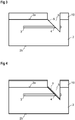
- Figure 2 shows a cross-sectional view of an intermediate product based on that shown in Figure 1 after an etching step.
- the pattern of the coating 10 of Figure 1 is transferred to the cladding layer 2 such that a channel 5 is formed.
- the channel 5 extends into the cladding layer 2 from the upper surface 2a at least to the optical axis OA that is defined by the extension direction of the waveguide structure 3.
- the optical axis corresponds to a propagation path of optical signals within the waveguide structure 3.
- the channel 5 is characterized by an angled sidewall surface 6 and a vertical sidewall surface 6a that is perpendicular or basically perpendicular to the upper surface 2a.
- the angled sidewall surface 6 forms an angle between 30° and 60° with respect to the optical axis OA.
- the angled sidewall surface 6 forms an angle of about 45° with both the optical axis OA and the upper surface 2a.
- the channel 5 is formed by also etching through the waveguide structure 3, hence a new end facet 4 is formed that is arranged flush with the angled sidewall surface 6.
- the coating 10 is removed or at least reduced in terms of its thickness during the etching.
- the latter means that a thin layer of the coating 10 remains on the upper surface 2a, as shown in this embodiment.
- a thickness of the coating 10 on the upper surface 2a is increased by application of additional coating material. Via a lithography step, for example, it is ensured that the channel 5 is free of any coating 10.
- Figure 4 shows a cross-sectional view of an intermediate product based on that shown in Figure 3 after deposition of dielectric material for forming a dielectric mirror 7 on the angled sidewall surface 6 of the channel 5.
- Deposition of the dielectric material comprises depositing dielectric layers with alternating refractive index regarding a wavelength of interest.
- the previously applied coating 10 ensures that the upper surface 2a is free from any dielectric material.
- the other sidewalls of the channel 5 can be coated with dielectric material.
- the coating 10 which can be understood as a lift off mask is removed for exposing the upper surface 2a.
- further steps such as cleaning steps can be performed.
- additional layers such as functional layers of a CMOS integrated circuit, can be applied on the upper surface 2a and/or the lower surface 2b.
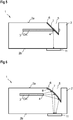
- FIG. 5 shows an exemplary embodiment of a semiconductor optical waveguide device 1 according to the improved concept.
- a light-sensitive device 11 such as a photodetector is arranged on the lower surface 2b.
- the dielectric mirror 7 acts as a deflector for deflecting optical signals from the optical axis OA inside the waveguide structure 3 onto a deflection path towards the light-sensitive device 11.
- the improved concept is analogously applicable if the light-sensitive device 11 is arranged at a distance from the lower surface 2b, for example as part of a separate semiconductor device that is directly bonded to the semiconductor optical waveguide device.
- the deflection path is perpendicular or basically perpendicular to the upper and lower surfaces 2a, 2b.
- the improved concept is easily applicable to other arrangements by choosing an appropriate angle of the angled sidewall surface 6.
- Figure 6 shows a further exemplary embodiment of a semiconductor optical waveguide device 1 according to the improved concept that is based on that shown in Figure 5 .
- the angled sidewall surface is realized as a curved surface as discussed above. This leads to the dielectric mirror 7 having a curved structure that corresponds to the curvature of the angled sidewall surface 6.
- the curved surface and interfaces of the dielectric layers of the dielectric mirror 7 result in the dielectric mirror 7 also acting as focusing element 8.
- the focusing character of the dielectric mirror 7 can be conveniently employed for compensating for a divergence of optical signals emitted from the end facet 4 of the waveguide structure 3.
- Compensating in this context means for example a focusing or collimation of the optical signals being deflected by the dielectric mirror 7 onto the deflection path.
- transferring the channel 5 to the cladding layer 2 does not comprise etching the waveguide structure 3 as its end facet 4 does not extend to or into the channel 5.
- the waveguide structure 3 is etched in advance of the transfer etch. Therefore, the waveguide structure 3 is emitting optical signals into the cladding layer 2 before impinging on the dielectric mirror 7.
- the channel 5, in particular the angled sidewall surface 6, is precisely transferred during the transfer etch due to the fact that only the oxide material of the cladding layer 2 is involved in the etch as the only material.
- the wave guide structure 3 remains protected as it is buried in the oxide material during the transfer etch.
- Figure 7 shows a cross-sectional view of an intermediate product of a further exemplary embodiment of the semiconductor optical waveguide device 1 according to the improved concept.
- the angled surface in the patterned coating 10 is oriented on the side of the patterned structure facing away from the waveguide structure 3.
- this geometry serves the purpose of deflecting optical signals from the optical axis OA towards the upper surface 2a instead of towards the lower surface 2b.
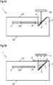
- Figure 9 showing a further exemplary embodiment of a semiconductor optical waveguide device 1.
- either configuration of the angled sidewall surface 6 and the dielectric mirror 7 can be chosen.
- the light-sensitive element 11 is arranged distant from the upper surface 2a, for example as a photodetector comprised by a further semiconductor device that is bonded to a surface of the semiconductor optical waveguide device 1.
- Figure 10 shows an alternative exemplary embodiment based on that of Figure 9 . Similar to Figure 6 , the end facet 4 of the waveguide structure 3 is arranged at a distance from the channel 5 such that it is not involved in the transfer etch for forming the channel 5. Again, this may lead to improved results due to a more uniform edge at the cost of a larger divergence at the location of the dielectric mirror 7.
- the angled sidewall surface 6 can be realized as a curved surface leading to a concavely shaped dielectric mirror 7. This is illustrated in Figure 11 . Similar to the embodiment of Figure 6 , this also leads to a compensation for the divergence, i.e. to a focusing or collimation of the optical signals being deflected onto the deflection path towards the upper surface 2a.
- Figure 12 illustrates that the improved concept is also applicable to applications in which the direction of light propagation is inverted.
- a light source 12 emits optical signals that are to be coupled into the waveguide structure 3.
- the concave shape of the dielectric mirror 7 also here compensates for a divergence and both deflects and focusses the optical signals onto the end facet 4 of the waveguide structure for efficient coupling.
- This concept can be applied analogously to other embodiments of the semiconductor optical waveguide device according to the improved concept, for example the embodiments illustrated in the previous figures.
- Figure 13 shows an embodiment similar to that of Figure 12 .
- the light source 12 is a collimated light source, such as a laser light source, therefore not requiring a curved shape of the dielectric mirror 7 as no divergence is to be compensated for.
- Figure 14 shows an alternative embodiment of a semiconductor optical waveguide device 1.
- the channel 5 is filled with an oxide material, in particular with an oxide material corresponding to that of the cladding layer 2 or with a material that has a refractive index closer to that of the cladding layer 2 compared to air.
- oxide material in particular with an oxide material corresponding to that of the cladding layer 2 or with a material that has a refractive index closer to that of the cladding layer 2 compared to air.
- Such materials include silicon dioxide, which is basically transparent for optical wavelengths of interest for many applications. Filling the channel 5 can lead to improved optical efficiencies due to avoidance of an oxide to gas interface possibly inducing back reflections.
- the embodiment of semiconductor optical waveguide device 1 further comprises an anti-reflective coating 9a.
- the anti-reflective coating 9a can further enhance optical efficiencies of the device by preventing optical losses caused by back reflections when optical signals impinge on the upper or lower surfaces 2a, 2b.
- Figure 15 shows a similar embodiment to that in Figure 14 with the difference that the focusing element 8 is realized as a lens element that is arranged on the upper surface 2a.
- the lens element can have an anti-reflective coating and serves the purpose of focusing and/or collimating optical signals, e.g. for compensating the aforementioned divergence.
- a lens element can be employed in combination with a curved, i.e. concave, dielectric mirror 7 for forming an optical telescope, for instance.
- Figure 16 shows a close up cross-sectional view of the channel 5 of an exemplary semiconductor optical waveguide device 1.
- a shielding layer 7a is deposited on the dielectric mirror 7.
- the shielding layer 7a is for example a metallic layer and serves the purpose of further reducing optical losses as well as a protective layer of the dielectric mirror 7.
- the shielding layer may be arranged between the dielectric mirror 7 and the angled sidewall surface 6.
- semiconductor optical waveguide device 1 shown in the figures represent exemplary embodiments, therefore they do not constitute a complete list of all embodiments according to the improved concept.
- Actual semiconductor optical waveguide devices may vary from the embodiments shown in terms of additional components and configuration, for instance.
- features shown in the various figures may be combined with each other and hence form additional embodiments according to the improved concept.
Landscapes
- Physics & Mathematics (AREA)
- General Physics & Mathematics (AREA)
- Optics & Photonics (AREA)
- Engineering & Computer Science (AREA)
- Microelectronics & Electronic Packaging (AREA)
- Optical Integrated Circuits (AREA)
Priority Applications (1)
| Application Number | Priority Date | Filing Date | Title |
|---|---|---|---|
| EP19219416.5A EP3842845A1 (fr) | 2019-12-23 | 2019-12-23 | Dispositif à semiconducteurs et procédé de fabrication de dispositif à semiconducteurs |
Applications Claiming Priority (1)
| Application Number | Priority Date | Filing Date | Title |
|---|---|---|---|
| EP19219416.5A EP3842845A1 (fr) | 2019-12-23 | 2019-12-23 | Dispositif à semiconducteurs et procédé de fabrication de dispositif à semiconducteurs |
Publications (1)
| Publication Number | Publication Date |
|---|---|
| EP3842845A1 true EP3842845A1 (fr) | 2021-06-30 |
Family
ID=69005618
Family Applications (1)
| Application Number | Title | Priority Date | Filing Date |
|---|---|---|---|
| EP19219416.5A Withdrawn EP3842845A1 (fr) | 2019-12-23 | 2019-12-23 | Dispositif à semiconducteurs et procédé de fabrication de dispositif à semiconducteurs |
Country Status (1)
| Country | Link |
|---|---|
| EP (1) | EP3842845A1 (fr) |
Cited By (1)
| Publication number | Priority date | Publication date | Assignee | Title |
|---|---|---|---|---|
| WO2023001665A1 (fr) * | 2021-07-23 | 2023-01-26 | Jenoptik Optical Systems Gmbh | Dispositif optique et procédé de production d'un dispositif optique |
Citations (4)
| Publication number | Priority date | Publication date | Assignee | Title |
|---|---|---|---|---|
| US20160109699A1 (en) * | 2014-10-15 | 2016-04-21 | Medlumics S.L. | Optical beam scanner |
| US20160306110A1 (en) * | 2015-04-20 | 2016-10-20 | Skorpios Technologies, Inc. | Vertical output couplers for photonic devices |
| US20170207600A1 (en) * | 2014-07-14 | 2017-07-20 | Biond Photonics Inc. | 3d photonic integration with light coupling elements |
| EP3330759A1 (fr) * | 2016-12-05 | 2018-06-06 | IMEC vzw | Coupleur de lumière à circuit photonique et procédé associé |
-
2019
- 2019-12-23 EP EP19219416.5A patent/EP3842845A1/fr not_active Withdrawn
Patent Citations (4)
| Publication number | Priority date | Publication date | Assignee | Title |
|---|---|---|---|---|
| US20170207600A1 (en) * | 2014-07-14 | 2017-07-20 | Biond Photonics Inc. | 3d photonic integration with light coupling elements |
| US20160109699A1 (en) * | 2014-10-15 | 2016-04-21 | Medlumics S.L. | Optical beam scanner |
| US20160306110A1 (en) * | 2015-04-20 | 2016-10-20 | Skorpios Technologies, Inc. | Vertical output couplers for photonic devices |
| EP3330759A1 (fr) * | 2016-12-05 | 2018-06-06 | IMEC vzw | Coupleur de lumière à circuit photonique et procédé associé |
Cited By (2)
| Publication number | Priority date | Publication date | Assignee | Title |
|---|---|---|---|---|
| WO2023001665A1 (fr) * | 2021-07-23 | 2023-01-26 | Jenoptik Optical Systems Gmbh | Dispositif optique et procédé de production d'un dispositif optique |
| DE102021119192B4 (de) | 2021-07-23 | 2024-04-11 | Jenoptik Optical Systems Gmbh | Optische Vorrichtung und Verfahren zum Herstellen einer optischen Vorrichtung |
Similar Documents
| Publication | Publication Date | Title |
|---|---|---|
| US6993225B2 (en) | Tapered structure for providing coupling between external optical device and planar optical waveguide and method of forming the same | |
| US9482816B2 (en) | Radiation coupler | |
| EP2803123B1 (fr) | Système de réseau à sous-longueur d'onde intégré | |
| KR100277695B1 (ko) | 에스 오 아이 광도파로를 이용한 하이브리드 광집적회로용 기판 제조방법 | |
| US11747529B2 (en) | Wafer level microstructures for an optical lens | |
| US7817883B2 (en) | Optical assembly and method of making same | |
| US10830951B2 (en) | Optical circuit and optical device | |
| AU2015258871B2 (en) | Optical connection of optical fibers to grating couplers | |
| US9020317B2 (en) | Surface waveguide having a tapered region and method of forming | |
| EP3293555B1 (fr) | Système optique de couplage de lumière en guide d'onde | |
| KR20060124721A (ko) | 실리콘 나노테이퍼 커플러 및 모드 정합 장치 | |
| JP2022508474A (ja) | 回折格子カプラ | |
| US10302871B2 (en) | Microfabricated fiber optic platform | |
| CN111527431B (zh) | 温度不敏感滤波器 | |
| JP3834024B2 (ja) | 光導波路部品及びその作製方法 | |
| KR100480280B1 (ko) | 광 하이브리드 모듈 및 그 제작방법 | |
| US20210263219A1 (en) | Planar Lightwave Circuit and Optical Device | |
| EP3842845A1 (fr) | Dispositif à semiconducteurs et procédé de fabrication de dispositif à semiconducteurs | |
| US20240159960A1 (en) | Heterogeneously integrated illuminator | |
| CN113359236A (zh) | 一种基于背向工艺的光栅耦合结构及制备方法 | |
| US6892010B2 (en) | Photodetector/optical fiber apparatus with enhanced optical coupling efficiency and method for forming the same | |
| US7466502B2 (en) | Optical wavelength division coupler and associated methods | |
| US5323407A (en) | Integrated optical mirror and its production process | |
| JP3857707B2 (ja) | 光デバイスの製造方法 | |
| JP7328582B2 (ja) | モノリシックミラーの作製方法 |
Legal Events
| Date | Code | Title | Description |
|---|---|---|---|
| PUAI | Public reference made under article 153(3) epc to a published international application that has entered the european phase |
Free format text: ORIGINAL CODE: 0009012 |
|
| STAA | Information on the status of an ep patent application or granted ep patent |
Free format text: STATUS: THE APPLICATION HAS BEEN PUBLISHED |
|
| AK | Designated contracting states |
Kind code of ref document: A1 Designated state(s): AL AT BE BG CH CY CZ DE DK EE ES FI FR GB GR HR HU IE IS IT LI LT LU LV MC MK MT NL NO PL PT RO RS SE SI SK SM TR |
|
| STAA | Information on the status of an ep patent application or granted ep patent |
Free format text: STATUS: THE APPLICATION IS DEEMED TO BE WITHDRAWN |
|
| 18D | Application deemed to be withdrawn |
Effective date: 20220104 |