EP3842866A1 - Messverfahren - Google Patents
Messverfahren Download PDFInfo
- Publication number
- EP3842866A1 EP3842866A1 EP19219624.4A EP19219624A EP3842866A1 EP 3842866 A1 EP3842866 A1 EP 3842866A1 EP 19219624 A EP19219624 A EP 19219624A EP 3842866 A1 EP3842866 A1 EP 3842866A1
- Authority
- EP
- European Patent Office
- Prior art keywords
- target
- features
- units
- feature
- image
- Prior art date
- Legal status (The legal status is an assumption and is not a legal conclusion. Google has not performed a legal analysis and makes no representation as to the accuracy of the status listed.)
- Withdrawn
Links
Images


Classifications
-
- G—PHYSICS
- G03—PHOTOGRAPHY; CINEMATOGRAPHY; ANALOGOUS TECHNIQUES USING WAVES OTHER THAN OPTICAL WAVES; ELECTROGRAPHY; HOLOGRAPHY
- G03F—PHOTOMECHANICAL PRODUCTION OF TEXTURED OR PATTERNED SURFACES, e.g. FOR PRINTING, FOR PROCESSING OF SEMICONDUCTOR DEVICES; MATERIALS THEREFOR; ORIGINALS THEREFOR; APPARATUS SPECIALLY ADAPTED THEREFOR
- G03F7/00—Photomechanical, e.g. photolithographic, production of textured or patterned surfaces, e.g. printing surfaces; Materials therefor, e.g. comprising photoresists; Apparatus specially adapted therefor
- G03F7/70—Microphotolithographic exposure; Apparatus therefor
- G03F7/70483—Information management; Active and passive control; Testing; Wafer monitoring, e.g. pattern monitoring
- G03F7/70605—Workpiece metrology
- G03F7/70616—Monitoring the printed patterns
- G03F7/70633—Overlay, i.e. relative alignment between patterns printed by separate exposures in different layers, or in the same layer in multiple exposures or stitching
-
- G—PHYSICS
- G03—PHOTOGRAPHY; CINEMATOGRAPHY; ANALOGOUS TECHNIQUES USING WAVES OTHER THAN OPTICAL WAVES; ELECTROGRAPHY; HOLOGRAPHY
- G03F—PHOTOMECHANICAL PRODUCTION OF TEXTURED OR PATTERNED SURFACES, e.g. FOR PRINTING, FOR PROCESSING OF SEMICONDUCTOR DEVICES; MATERIALS THEREFOR; ORIGINALS THEREFOR; APPARATUS SPECIALLY ADAPTED THEREFOR
- G03F7/00—Photomechanical, e.g. photolithographic, production of textured or patterned surfaces, e.g. printing surfaces; Materials therefor, e.g. comprising photoresists; Apparatus specially adapted therefor
- G03F7/70—Microphotolithographic exposure; Apparatus therefor
- G03F7/70483—Information management; Active and passive control; Testing; Wafer monitoring, e.g. pattern monitoring
- G03F7/70605—Workpiece metrology
- G03F7/70616—Monitoring the printed patterns
- G03F7/70625—Dimensions, e.g. line width, critical dimension [CD], profile, sidewall angle or edge roughness
-
- G—PHYSICS
- G03—PHOTOGRAPHY; CINEMATOGRAPHY; ANALOGOUS TECHNIQUES USING WAVES OTHER THAN OPTICAL WAVES; ELECTROGRAPHY; HOLOGRAPHY
- G03F—PHOTOMECHANICAL PRODUCTION OF TEXTURED OR PATTERNED SURFACES, e.g. FOR PRINTING, FOR PROCESSING OF SEMICONDUCTOR DEVICES; MATERIALS THEREFOR; ORIGINALS THEREFOR; APPARATUS SPECIALLY ADAPTED THEREFOR
- G03F7/00—Photomechanical, e.g. photolithographic, production of textured or patterned surfaces, e.g. printing surfaces; Materials therefor, e.g. comprising photoresists; Apparatus specially adapted therefor
- G03F7/70—Microphotolithographic exposure; Apparatus therefor
- G03F7/70483—Information management; Active and passive control; Testing; Wafer monitoring, e.g. pattern monitoring
- G03F7/70605—Workpiece metrology
- G03F7/70681—Metrology strategies
- G03F7/70683—Mark designs
-
- G—PHYSICS
- G06—COMPUTING OR CALCULATING; COUNTING
- G06T—IMAGE DATA PROCESSING OR GENERATION, IN GENERAL
- G06T7/00—Image analysis
- G06T7/0002—Inspection of images, e.g. flaw detection
- G06T7/0004—Industrial image inspection
- G06T7/001—Industrial image inspection using an image reference approach
-
- G—PHYSICS
- G06—COMPUTING OR CALCULATING; COUNTING
- G06T—IMAGE DATA PROCESSING OR GENERATION, IN GENERAL
- G06T7/00—Image analysis
- G06T7/10—Segmentation; Edge detection
- G06T7/13—Edge detection
-
- G—PHYSICS
- G06—COMPUTING OR CALCULATING; COUNTING
- G06T—IMAGE DATA PROCESSING OR GENERATION, IN GENERAL
- G06T7/00—Image analysis
- G06T7/10—Segmentation; Edge detection
- G06T7/194—Segmentation; Edge detection involving foreground-background segmentation
-
- G—PHYSICS
- G06—COMPUTING OR CALCULATING; COUNTING
- G06T—IMAGE DATA PROCESSING OR GENERATION, IN GENERAL
- G06T2207/00—Indexing scheme for image analysis or image enhancement
- G06T2207/10—Image acquisition modality
- G06T2207/10056—Microscopic image
- G06T2207/10061—Microscopic image from scanning electron microscope
-
- G—PHYSICS
- G06—COMPUTING OR CALCULATING; COUNTING
- G06T—IMAGE DATA PROCESSING OR GENERATION, IN GENERAL
- G06T2207/00—Indexing scheme for image analysis or image enhancement
- G06T2207/30—Subject of image; Context of image processing
- G06T2207/30108—Industrial image inspection
- G06T2207/30148—Semiconductor; IC; Wafer
Definitions
- the present disclosure relates to metrology methods and targets, in particular for device manufacturing using lithographic apparatus.
- a lithographic apparatus is a machine that applies a desired pattern onto a substrate, usually onto a target portion of the substrate.
- a lithographic apparatus can be used, for example, in the manufacture of integrated circuits (ICs).
- a patterning device which is alternatively referred to as a mask or a reticle, may be used to generate a circuit pattern to be formed on an individual layer of the IC.
- This pattern can be transferred onto a target portion (e.g. including part of a die, one die, or several dies) on a substrate (e.g., a silicon wafer). Transfer of the pattern is typically via imaging onto a layer of radiation-sensitive material (resist) provided on the substrate.
- a single substrate will contain a network of adjacent target portions that are successively patterned.
- EPE edge placement error
- Overlay can arise from a variety of causes in the lithographic process, for example errors in the positioning of the substrate during exposure and aberrations in the projected image. Overlay can also be caused during process steps, such as etching, which are used to transfer the pattern into the substrate. Some such process steps generate stresses within the substrate that lead to local or global distortions of the substrate. The formation of three dimensional structures on the substrate, such as is required for recently developed memory types and MEMS, can also lead to significant distortions of the substrate. CD variation can also derive from a variety of causes, including dose or focus errors.
- the present disclosure aims to provide improved metrology methods, e.g. for use in lithographic device manufacturing processes.
- Electronic devices are constructed of circuits formed on a piece of silicon called a substrate. Many circuits may be formed together on the same piece of silicon and are called integrated circuits or ICs. The size of these circuits has decreased dramatically so that many more of them can fit on the substrate. For example, an IC chip in a smartphone can be as small as a thumbnail and yet may include over 2 billion transistors, the size of each transistor being less than 1/1000th the size of a human hair.
- One component of improving yield is monitoring the chip-making process to ensure that it is producing a sufficient number of functional integrated circuits.
- One way to monitor the process is to inspect the chip circuit structures at various stages of their formation. Inspection can be carried out using a scanning electron microscope (SEM), an optical inspection system, etc. Such systems can be used to image these structures, in effect, taking a "picture" of the structures of the wafer, with a SEM being able to image the smallest of these structures. The image can be used to determine if the structure was formed properly in the proper location. If the structure is defective, then the process can be adjusted, so the defect is less likely to recur.
- SEM scanning electron microscope
- targets are easier to image than the device features, it is still difficult to make accurate measurements of absolute distances in those images, especially if different imaging devices are used or if the features are measured at different stages in the manufacturing process.
- each target has multiple target sub-units all of which have the same two features but in different target sub-units one of the features is located at a different position relative to the other. Because of the range of relative positions of the two features, a positional error will cause an overlap of the edges of the two features in at least one of the targets. Knowing the initial positional variations, the size of the positional error can be determined by identifying in which target the two features' edges overlap. In other examples, the positional error can be determined by comparing images of different sub-units, possibly after cropping, rotation and/or reflection of one image. Thus it is no longer necessary to make a direct measurement of the position of two features and a more accurate determination of the size of an error can be achieved.
- FIG. 1 illustrates a typical layout of a semiconductor production facility.
- a lithographic apparatus 100 applies a desired pattern onto a substrate.
- a lithographic apparatus is used, for example, in the manufacture of integrated circuits (ICs).
- a patterning device MA which is alternatively referred to as a mask or a reticle, comprises a circuit pattern of features (often referred to as "product features") to be formed on an individual layer of the IC.
- This pattern is transferred onto a target portion (e.g., comprising part of, one, or several dies) on a substrate 'W' (e.g., a silicon wafer) via exposure 104 of the patterning device onto a layer of radiation-sensitive material (resist) provided on the substrate.
- a single substrate will contain a network of adjacent target portions that are successively patterned.
- lithographic apparatus irradiate each target portion by illuminating the patterning device while synchronously positioning the target portion of the substrate at an image position of the patterning device.
- An irradiated target portion of the substrate is referred to as an "exposure field", or simply "field".
- the layout of the fields on the substrate is typically a network of adjacent rectangles or other shapes aligned in accordance to a Cartesian two-dimensional coordinate system (e.g. aligned along an X and an Y-axis, both axes being orthogonal to each other).
- a requirement on the lithographic apparatus is an accurate reproduction of the desired pattern onto the substrate.
- the positions and dimensions of the applied product features need to be within certain tolerances. Position errors may give rise to an overlay error (often referred to as "overlay").
- overlay is the error in placing a first product feature within a first layer relative to a second product feature within a second layer.
- the lithographic apparatus reduces the overlay errors by aligning each wafer accurately to a reference prior to patterning. This is done by measuring positions of alignment marks which are applied to the substrate. Based on the alignment measurements the substrate position is controlled during the patterning process in order to prevent occurrence of out of tolerance overlay errors. Alignment marks are typically created as part of the product image forming the reference to which overlay is measured. Alternatively alignment marks of a previously formed layer can be used.
- An error in a critical dimension (CD) of the product feature may occur when the applied dose associated with the exposure 104 is not within specification. For this reason the lithographic apparatus 100 must be able to accurately control the dose of the radiation applied to the substrate. CD errors may also occur when the substrate is not positioned correctly with respect to a focal plane associated with the pattern image. Focal position errors are commonly associated with non-planarity of a substrate surface. The lithographic apparatus reduces these focal position errors by measuring the substrate surface topography using a level sensor prior to patterning. Substrate height corrections are applied during subsequent patterning to assure correct imaging (focusing) of the patterning device onto the substrate.
- a metrology apparatus 140 To verify the overlay and CD errors associated with the lithographic process the patterned substrates are inspected by a metrology apparatus 140.
- a metrology apparatus Common examples of a metrology apparatus are scatterometers and scanning electron microscopes.
- the scatterometer conventionally measures characteristics of dedicated metrology targets. These metrology targets are representative of the product features, except that their dimensions are typically larger in order to allow accurate measurement.
- the scatterometer measures the overlay by detecting an asymmetry of a diffraction pattern associated with an overlay metrology target. Critical dimensions are measured by analysis of a diffraction pattern associated with a CD metrology target.
- a CD metrology target is used for measuring the result of the most recently exposed layer.
- An overlay target is used for measuring the difference between the positions of the previous and most recent layers.
- An electron beam (e-beam) based inspection tool such as a scanning electron microscope (SEM) can often provide superior results in the measurement of small overlay and CD values.
- SEM scanning electron microscope
- lithographic apparatus 100 and metrology apparatus 140 form part of a "litho cell" or “litho cluster".
- the litho cluster comprises also a coating apparatus 108 for applying photosensitive resist to substrates W, a baking apparatus 110, a developing apparatus 112 for developing the exposed pattern into a physical resist pattern, an etching station 122, apparatus 124 performing a post-etch annealing step and possibly further processing apparatuses, 126, etc..
- the metrology apparatus is configured to inspect substrates after development 112 or after further processing (e.g. etching).
- the various apparatus within the litho cell are controlled by a supervisory control system SCS, which issues control signals 166 to control the lithographic apparatus via lithographic apparatus control unit LACU 106 to perform recipe R.
- the SCS allows the different apparatuses to be operated giving maximum throughput and product yield.
- An important control mechanism is the feedback 146 of the metrology apparatus 140 to the various apparatus (via the SCS), in particular to the lithographic apparatus 100. Based on the characteristics of the metrology feedback corrective actions are determined to improve processing quality of subsequent substrates.
- the SCS can be one computer or multiple computers, which may or may not communicate.
- the recipe R can be implemented as one recipe or as multiple independent recipes.
- the recipe for a process step such as etch may be totally independent of the recipe to inspect the result of that process step (e.g. etch).
- two or more recipes for individual steps may be interrelated such that one recipe is adjusted to take account of the results of performance of another recipe on the same or a different substrate.
- the performance of a lithographic apparatus is conventionally controlled and corrected by methods such as advanced process control (APC) described for example in US2012008127A1 .
- the advanced process control techniques use measurements of metrology targets applied to the substrate.
- a Manufacturing Execution System (MES) schedules the APC measurements and communicates the measurement results to a data processing unit.
- the data processing unit translates the characteristics of the measurement data to a recipe comprising instructions for the lithographic apparatus. This method is very effective in suppressing drift phenomena associated with the lithographic apparatus.
- the processing of metrology data to corrective actions performed by the processing apparatus is important for semiconductor manufacturing.
- characteristics of individual patterning devices, substrates, processing apparatus and other context data may be needed to further optimize the manufacturing process.
- the framework wherein available metrology and context data is used to optimize the lithographic process as a whole is commonly referred to as part of holistic lithography.
- context data relating to CD errors on a reticle may be used to control various apparatus (lithographic apparatus, etching station) such that said CD errors will not affect the yield of the manufacturing process.
- Subsequent metrology data may then be used to verify the effectiveness of the control strategy and further corrective actions may be determined.
- EPE edge placement error
- EPE is very important to ensure a semiconductor device is working properly, for example it may affect whether, in a back end of line module, there is sufficient electrical contact. This makes EPE measurements very valuable to ensuring the process window accommodates a sufficient EPE budget and to controlling the process to remain within window.
- a target design to facilitate EPE determination e.g. after etch
- a measurement after etch can be desirable because it better represents the final patterned structure.
- after-etch measurement sees the contributions of the etcher and other tools, such as deposition and CMP, to the final pattern.
- a measurement after development (before pattern transfer) is also desirable as it may enable defective exposures to be reworked rather than scrapped.
- the target corresponds to a pattern of interest but a part of the pattern has a displacement offset or bias.
- the target has components (features) in the same two layers as the pattern of interest and the target features in each layer correspond to the device features in the corresponding layer.
- the device features may also be referred to as product features or pattern features.
- either or both features of the target correspond exactly to device features of interest.
- OPC optical proximity correction
- the target features have the same pitch as the device features (e.g. dense, semi-dense or isolated).
- Desirably the target features have the same CD as the device features.
- the target feature need not be as long as the device feature but the target feature is desirably long enough to behave similarly to the device feature.
- the device has an array of features, e.g. parallel lines or a grid of contact holes, the target need not have the same extent as the array of device features but desirably has at least two unit cells of the array.
- the target has a plurality of parts, referred to herein as target units.
- the various target units provide a range of different offsets between the two features. This enables the self-calibration of metrology by designing multiple displacement offsets on the reticle level which allows the direct determining of the recipe accuracy. Desirably all subunits of the target fit within the field of view of a metrology tool that is to be used to measure the target. For example the target can be smaller than 40 ⁇ m by 40 ⁇ m.
- the various target units need not be demarcated by structure. For example if a first target feature comprises elongated lines and a second target feature is a cut feature, the several target units may be formed by cut features positioned along a continuous set of lines.
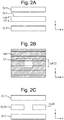
- Figure 2A shows three lines DL1-3 in the line layer and Figure 2B shows the cut feature C1 formed in a hardmask HM or lithography stack (e.g. resist, adhesion layer, BARC, etc.).
- Figure 2C shows the line layer after etching: line DL2 is split into two lines DL2A and DL2B.
- CD-y means the critical dimension in the y-direction
- overlay-y means overlay in the y-direction.
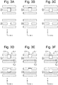
- Figures 3A to C in which the top parts show the situation after development and the bottom parts show the situation after etch. It can be seen that small variations in the position of the cut feature that are detectable in after-development inspection do not result in any detectable difference in the after-etch inspection results because the cut feature is bigger than the line.
- a target unit according to an embodiment is shown in Figure 3D , in which the top part shows the situation after development and the bottom part shows the situation after etch.
- the target unit corresponds to the device features except that the cut-layer origin is displaced in the y-direction by line pitch/2.
- the target cut feature CT1 overlaps two target line features TL1, TL2 symmetrically but incompletely so that each target line is half-cut. Edges of the target cut feature CT1 fall within the target line features TL1, TL2. This has the effect that the cut CD-y is clearly detectable in the target layout after etch.
- the target feature is positioned so that its relevant edges are detectable after processing.
- Figures 3E and 3F show the effect of an overlay error in the +y and -y directions respectively, again the top parts show the situation after development and the bottom parts show the situation after etch.
- the effect of an overlay error is that the half-cut in one of the target lines increases while the other decreases. Therefore, the direction (positive or negative) of an overlay error can be determined without requiring measurements of images of the target, simply by considering in which direction the target is asymmetric.
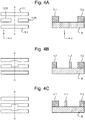
- Figures 4A to C show on the left a plan view and on the right a cross-section of the situation after etching of the cut feature.
- a magnitude of a positional error - such as overlay, CD or edge placement error - it is possible to make use of any symmetry in the target.
- a positional error - such as overlay, CD or edge placement error -
- an image of the target with overlay-y of -A nm rotated by 180° looks like an image of a target with overlay-y of +A nm.
- the same effect can be achieved by reflecting one of the images. Therefore, by providing a plurality of targets with different biases (displacements of the second target feature at mask level) and checking for symmetric pairs the magnitude of an actual overlay can be determined.
- the above approach does not require a measurement of an absolute distance in the images provided by the metrology tool and can thus be considered self-calibrating.
- This approach can also be applied to non-imaging metrology tools, such as scatterometers.
- the desired range of measurement and resolution can be set by appropriate selection of the number of targets and size of the variation in bias (e.g. ⁇ n ⁇ 0.5 nm, ⁇ n ⁇ 1 nm, ⁇ n ⁇ 2 nm).
- the values of n are such that the range of offsets in each direction is comparable to the distance between the nominal positions of adjacent edges of the two target features (which desirably corresponds to the distance between the nominal positions of edges of two device features).
- the nominal position of a feature or edge is its position if correctly imaged and may also be referred to as the design position.
- Figure 7 shows an example of an array of target units TU1, TU2, ... TUn.
- Each target unit can have dimensions less than about 5 ⁇ m by 5 ⁇ m, e.g. 2 ⁇ m by 2 ⁇ m.
- An array of 9 or more target units can easily fit within the field of view of a metrology tool enabling overlay and/or CD to be determined with a single measurement.
- the array of target units can easily fit within a scribe lane or within product areas if appropriate.
- a target having lines extending in the x-direction for measuring CD and overlay in the y-direction Whilst a target having lines extending in the x-direction for measuring CD and overlay in the y-direction has been illustrated, it will be appreciated that the whole arrangement can be rotated 90° to measure overlay and CD in the x-direction.
- a composite target might include target units of both orientations.
- a device layer having only or predominately lines extending in x or y it may be sufficient to measure overlay and CD in one direction only.
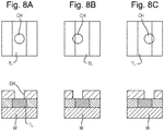
- FIG. 8A to C Another set of target units is shown in Figures 8A to C for use with a pattern of contact holes (vias) that are to contact lines.
- the top part is a plan view and the bottom part a corresponding cross-section.
- the contact hole CH is aligned with the center of the target line feature TL (which in this example extends in the y direction).
- the contact hole feature CH has a predetermined offset in the -ve x-direction
- the third target unit Figure 8C
- the contact hole feature CH has a predetermined offset in the +ve x-direction.
- the size of the contact hole and the offsets in the second and third target units are chosen so that with fully correct imaging and patterning (i.e. overlay and CD well within process window) no edge of the underlying line is visible in the first target unit but the edge is visible in the second and third target units. If there is an overlay error of sufficient magnitude shifting the contact hole target features in the +ve x-direction relative to the line feature, then the edge of the line feature will become visible in the contact hole of the first target unit and disappear from the contact hole target feature of the second target unit. Conversely an overlay error in the -x direction will cause the edge of the line feature to appear in the first target unit and dis-appear in the third target unit.
- a -ve CD error of sufficient magnitude cause the edges to appear in the first target unit and move in the second and third target units.
- a +ve CD error would cause the edges of the line feature to disappear from both the second and third target units. Thud different types of errors can be distinguished between by consideration of in which target units edges are visible. Provision of additional target units with different offsets can enable detection of different types of error and different magnitudes of error over a wider range and/or with higher resolution.
- EPE can be determined without requiring any precise measurements.
- EPE is an error in a location of an edge of a first target with an edge of a second target.
- a cut hole is targeted to be placed on a metal line with an outer edge of the cut located 3nm from an edge of the metal line.
- the metal line is oversized by 1nm and the cut hole is placed 1nm too close to the line edge. In this case, the EPE is zero because the two errors cancel each other out.
- the metal line is oversized by 1nm and the cut hole is placed 1nm too far from the line edge.
- the EPE is 2nm because the two errors are additive.
- an array of targets with biases as described above are printed.
- the edge of the cut aligns with the edge of the metal (including the overlay error and CD error). This is determined by inspecting the array of targets, where the cut can be seen getting closer to the edge of the metal line, as can be seen between Fig. 3D where the top edge of CT1 is in the middle of TL1, and in Fig. 3E where the top edge of CT1 is closer to the top edge of TL1.
- the top edge of CD1 will get closer to the top edge of TL1 and, at one of the biases, the two edges will align. As the array of targets continues, the top edge of CT1 will go beyond the top of TL1. Based on the first of the array of targets where CT1 cuts through TL1, the EPE can be determined just by knowing the bias of that particular target.
- Figures 9A to C illustrate an embodiment applied to a pattern of upper channel holes CH2 (e.g. memory channel holes in a 3D-NAND device) that are to be placed above lower channel holes CH1 as shown in Figure 9A .
- Accurate alignment of the two layers of channel holes is desirable to ensure a good electrical connection.
- Figure 9B is a schematic view of a target unit comprising an array of channel hole features in the after-etch situation in a case with good alignment.
- Figure 9C shows a corresponding view in a mis-aligned example: only a part of the edge of the lower contact hole is visible.
- a target for use with such a pattern comprises a plurality of target holes in the upper layer at a variety of offsets relative to the channel holes in the lower layer.
- the offsets may include offsets in the x-direction, the y-direction and/or both x- and y-directions.
- FIG. 10 An exemplary method is depicted in Figure 10 , which is a flow chart.
- a first layer L1 is exposed S1, then developed and processed (e.g. by etching) S2.
- the line features are formed in these steps.
- the lower channel holes are formed.
- a second layer L2 is exposed S2, then developed and processed (e.g. by etching) S4.
- the cut features are formed in these steps.
- the contact hole features are formed in these steps.
- the upper contact holes are formed.
- the first layer L1 includes first target features of the plurality of target units and the second layer L2 includes second target features of the plurality of target units.
- the target units are then measured S5, e.g. using a scanning electron microscope. Desirably all target units are imaged in a single image generated by the metrology tool. Based on the measurement results, any edge placement errors (EPE) are detected and characterized, e.g. by detecting the presence and/or position of edges in the image(s) of target units or by considering the symmetry of processed (e.g. cropped, rotated and/or reflected) images and normal images of different target units. In the event that out-of-budget edge placement errors are detected, appropriate process corrections are determined S7 and fed back to the expose and develop/process steps S1-S4.
- EPE edge placement errors
- the techniques disclosed herein can provide self-calibrating targets, e.g. for detecting edge placement errors using scanning electron microscopes or scatterometry-based metrology tools. These self-calibrating targets can provide improved accuracy and avoid the need for a tool-of-reference.
- the techniques disclosed herein can enable multiple EPE parameters to be extracted in one metrology step which improves processing cycle time.
- the techniques disclosed herein can reduce the need for very high-voltage SEM so the measurement is less destructive.
- An embodiment may include a computer program containing one or more sequences of machine-readable instructions configured to instruct various apparatus as depicted in Figure 1 to perform measurement and optimization steps and to control a subsequent exposure process as described above.
- This computer program may be executed, for example, within the control unit LACU or the supervisory control system SCS of Figure 1 or a combination of both.
- a data storage medium e.g., semiconductor memory, magnetic or optical disk having such a computer program stored therein.
- imprint lithography a topography in a patterning device defines the pattern created on a substrate.
- the topography of the patterning device may be pressed into a layer of resist supplied to the substrate whereupon the resist is cured by applying electromagnetic radiation, heat, pressure or a combination thereof.
- the patterning device is moved out of the resist leaving a pattern in it after the resist is cured.
- UV radiation e.g., having a wavelength of or about 365, 355, 248, 193, 157 or 126 nm
- EUV radiation e.g., having a wavelength in the range of 1-100 nm
- particle beams such as ion beams or electron beams.
- lens may refer to any one or combination of various types of optical components, including refractive, reflective, magnetic, electromagnetic and electrostatic optical components. Reflective components are likely to be used in an apparatus operating in the UV and/or EUV ranges.
- the term "or" encompasses all possible combinations, except where infeasible. For example, if it is stated that a component may include A or B, then, unless specifically stated otherwise or infeasible, the component may include A, or B, or A and B. As a second example, if it is stated that a component may include A, B, or C, then, unless specifically stated otherwise or infeasible, the component may include A, or B, or C, or A and B, or A and C, or B and C, or A and B and C.
Landscapes
- Physics & Mathematics (AREA)
- General Physics & Mathematics (AREA)
- Engineering & Computer Science (AREA)
- Computer Vision & Pattern Recognition (AREA)
- Theoretical Computer Science (AREA)
- Quality & Reliability (AREA)
- Exposure And Positioning Against Photoresist Photosensitive Materials (AREA)
- Eyeglasses (AREA)
Priority Applications (5)
| Application Number | Priority Date | Filing Date | Title |
|---|---|---|---|
| EP19219624.4A EP3842866A1 (de) | 2019-12-24 | 2019-12-24 | Messverfahren |
| TW109144631A TWI820371B (zh) | 2019-12-24 | 2020-12-17 | 用於微影裝置製造程序之檢測工具及度量衡方法 |
| US17/789,160 US20230035488A1 (en) | 2019-12-24 | 2020-12-19 | Metrology method |
| CN202080089819.3A CN114846411B (zh) | 2019-12-24 | 2020-12-19 | 量测方法 |
| PCT/EP2020/087345 WO2021130142A1 (en) | 2019-12-24 | 2020-12-19 | Metrology method |
Applications Claiming Priority (1)
| Application Number | Priority Date | Filing Date | Title |
|---|---|---|---|
| EP19219624.4A EP3842866A1 (de) | 2019-12-24 | 2019-12-24 | Messverfahren |
Publications (1)
| Publication Number | Publication Date |
|---|---|
| EP3842866A1 true EP3842866A1 (de) | 2021-06-30 |
Family
ID=69024179
Family Applications (1)
| Application Number | Title | Priority Date | Filing Date |
|---|---|---|---|
| EP19219624.4A Withdrawn EP3842866A1 (de) | 2019-12-24 | 2019-12-24 | Messverfahren |
Country Status (5)
| Country | Link |
|---|---|
| US (1) | US20230035488A1 (de) |
| EP (1) | EP3842866A1 (de) |
| CN (1) | CN114846411B (de) |
| TW (1) | TWI820371B (de) |
| WO (1) | WO2021130142A1 (de) |
Families Citing this family (3)
| Publication number | Priority date | Publication date | Assignee | Title |
|---|---|---|---|---|
| EP4338009A4 (de) * | 2021-10-21 | 2025-06-04 | KLA Corporation | Induzierte verschiebungen für verbesserte überlagerungsfehlermetrologie |
| CN116051550B (zh) * | 2023-03-29 | 2023-07-04 | 长鑫存储技术有限公司 | 图案检测方法及图案检测系统 |
| US20250279371A1 (en) * | 2024-03-04 | 2025-09-04 | Semiconductor Components Industries, Llc | Fiducial designs and related methods for wire bond pattern recognition |
Citations (3)
| Publication number | Priority date | Publication date | Assignee | Title |
|---|---|---|---|---|
| US20120008127A1 (en) | 2010-07-09 | 2012-01-12 | Asml Netherlands B.V. | Method Of Calibrating A Lithographic Apparatus, Device Manufacturing Method and Associated Data Processing Apparatus and Computer Program Product |
| US20170010541A1 (en) * | 2014-02-17 | 2017-01-12 | Asml Netherlands B.V. | Method of determining edge placement error, inspection apparatus, patterning device, substrate and device manufacturing method |
| WO2019115391A1 (en) * | 2017-12-11 | 2019-06-20 | Asml Netherlands B.V. | Voltage contrast metrology mark |
Family Cites Families (6)
| Publication number | Priority date | Publication date | Assignee | Title |
|---|---|---|---|---|
| WO2005116577A1 (ja) * | 2004-05-28 | 2005-12-08 | Nikon Corporation | 結像光学系の調整方法、結像装置、位置ずれ検出装置、マ-ク識別装置及びエッジ位置検出装置 |
| US9595419B1 (en) * | 2013-11-27 | 2017-03-14 | Multibeam Corporation | Alignment and registration targets for multiple-column charged particle beam lithography and inspection |
| CN106164778B (zh) * | 2014-04-28 | 2018-02-09 | Asml荷兰有限公司 | 估计图案形成装置的变形和/或其位置的改变 |
| WO2017212035A1 (en) * | 2016-06-10 | 2017-12-14 | Imec Vzw | Metrology method and apparatus for a semiconductor manufacturing process |
| KR102711288B1 (ko) * | 2016-08-17 | 2024-09-27 | 삼성전자주식회사 | 결함 검사 방법 및 결함 검사 장치 |
| US10533848B2 (en) * | 2018-03-05 | 2020-01-14 | Kla-Tencor Corporation | Metrology and control of overlay and edge placement errors |
-
2019
- 2019-12-24 EP EP19219624.4A patent/EP3842866A1/de not_active Withdrawn
-
2020
- 2020-12-17 TW TW109144631A patent/TWI820371B/zh active
- 2020-12-19 WO PCT/EP2020/087345 patent/WO2021130142A1/en not_active Ceased
- 2020-12-19 US US17/789,160 patent/US20230035488A1/en active Pending
- 2020-12-19 CN CN202080089819.3A patent/CN114846411B/zh active Active
Patent Citations (3)
| Publication number | Priority date | Publication date | Assignee | Title |
|---|---|---|---|---|
| US20120008127A1 (en) | 2010-07-09 | 2012-01-12 | Asml Netherlands B.V. | Method Of Calibrating A Lithographic Apparatus, Device Manufacturing Method and Associated Data Processing Apparatus and Computer Program Product |
| US20170010541A1 (en) * | 2014-02-17 | 2017-01-12 | Asml Netherlands B.V. | Method of determining edge placement error, inspection apparatus, patterning device, substrate and device manufacturing method |
| WO2019115391A1 (en) * | 2017-12-11 | 2019-06-20 | Asml Netherlands B.V. | Voltage contrast metrology mark |
Also Published As
| Publication number | Publication date |
|---|---|
| WO2021130142A1 (en) | 2021-07-01 |
| TWI820371B (zh) | 2023-11-01 |
| CN114846411B (zh) | 2026-04-24 |
| CN114846411A (zh) | 2022-08-02 |
| TW202132907A (zh) | 2021-09-01 |
| US20230035488A1 (en) | 2023-02-02 |
Similar Documents
| Publication | Publication Date | Title |
|---|---|---|
| US8804137B2 (en) | Unique mark and method to determine critical dimension uniformity and registration of reticles combined with wafer overlay capability | |
| CN113253578A (zh) | 用于光刻过程的优化的方法 | |
| EP3495889A1 (de) | Verfahren zur steuerung einer fertigungsvorrichtung und zugehörige vorrichtungen | |
| US11061336B2 (en) | Device manufacturing method | |
| US20230035488A1 (en) | Metrology method | |
| US8010307B2 (en) | In-line overlay measurement using charged particle beam system | |
| JP7749047B2 (ja) | マルチステッププロセス検査方法 | |
| EP3396457A1 (de) | Verfahren zur herstellung einer vorrichtung | |
| JP2003017386A (ja) | 位置合わせ方法、露光方法、露光装置及びデバイスの製造方法 | |
| JP2020512582A (ja) | 基板の応力を決定する方法、リソグラフィプロセス、リソグラフィ装置、及びコンピュータプログラム製品を制御するための制御システム | |
| CN115668060A (zh) | 用于优化采样方案的方法和相关设备 | |
| US20260104650A1 (en) | Method of tilt metrology and associated apparatuses | |
| EP3376290A1 (de) | Metrologieverfahren und verfahren zur vorrichtungsherstellung | |
| EP4298481A1 (de) | Neuartige schnittstellendefinition für lithografische vorrichtung |
Legal Events
| Date | Code | Title | Description |
|---|---|---|---|
| PUAI | Public reference made under article 153(3) epc to a published international application that has entered the european phase |
Free format text: ORIGINAL CODE: 0009012 |
|
| STAA | Information on the status of an ep patent application or granted ep patent |
Free format text: STATUS: THE APPLICATION HAS BEEN PUBLISHED |
|
| AK | Designated contracting states |
Kind code of ref document: A1 Designated state(s): AL AT BE BG CH CY CZ DE DK EE ES FI FR GB GR HR HU IE IS IT LI LT LU LV MC MK MT NL NO PL PT RO RS SE SI SK SM TR |
|
| STAA | Information on the status of an ep patent application or granted ep patent |
Free format text: STATUS: THE APPLICATION IS DEEMED TO BE WITHDRAWN |
|
| 18D | Application deemed to be withdrawn |
Effective date: 20220104 |