EP3843158B1 - Vorrichtung umfassend transistoren mit rundum-gate und herstellungsverfahren einer solchen vorrichtung - Google Patents
Vorrichtung umfassend transistoren mit rundum-gate und herstellungsverfahren einer solchen vorrichtung Download PDFInfo
- Publication number
- EP3843158B1 EP3843158B1 EP20216818.3A EP20216818A EP3843158B1 EP 3843158 B1 EP3843158 B1 EP 3843158B1 EP 20216818 A EP20216818 A EP 20216818A EP 3843158 B1 EP3843158 B1 EP 3843158B1
- Authority
- EP
- European Patent Office
- Prior art keywords
- transistors
- sources
- drains
- level
- layer
- Prior art date
- Legal status (The legal status is an assumption and is not a legal conclusion. Google has not performed a legal analysis and makes no representation as to the accuracy of the status listed.)
- Active
Links
Images


















Classifications
-
- H—ELECTRICITY
- H10—SEMICONDUCTOR DEVICES; ELECTRIC SOLID-STATE DEVICES NOT OTHERWISE PROVIDED FOR
- H10B—ELECTRONIC MEMORY DEVICES
- H10B63/00—Resistance change memory devices, e.g. resistive RAM [ReRAM] devices
- H10B63/30—Resistance change memory devices, e.g. resistive RAM [ReRAM] devices comprising selection components having three or more electrodes, e.g. transistors
-
- H—ELECTRICITY
- H10—SEMICONDUCTOR DEVICES; ELECTRIC SOLID-STATE DEVICES NOT OTHERWISE PROVIDED FOR
- H10B—ELECTRONIC MEMORY DEVICES
- H10B63/00—Resistance change memory devices, e.g. resistive RAM [ReRAM] devices
- H10B63/80—Arrangements comprising multiple bistable or multi-stable switching components of the same type on a plane parallel to the substrate, e.g. cross-point arrays
- H10B63/84—Arrangements comprising multiple bistable or multi-stable switching components of the same type on a plane parallel to the substrate, e.g. cross-point arrays arranged in a direction perpendicular to the substrate, e.g. 3D cell arrays
- H10B63/845—Arrangements comprising multiple bistable or multi-stable switching components of the same type on a plane parallel to the substrate, e.g. cross-point arrays arranged in a direction perpendicular to the substrate, e.g. 3D cell arrays the switching components being connected to a common vertical conductor
-
- H—ELECTRICITY
- H10—SEMICONDUCTOR DEVICES; ELECTRIC SOLID-STATE DEVICES NOT OTHERWISE PROVIDED FOR
- H10D—INORGANIC ELECTRIC SEMICONDUCTOR DEVICES
- H10D30/00—Field-effect transistors [FET]
- H10D30/01—Manufacture or treatment
- H10D30/014—Manufacture or treatment of FETs having zero-dimensional [0D] or one-dimensional [1D] channels, e.g. quantum wire FETs, single-electron transistors [SET] or Coulomb blockade transistors
-
- H—ELECTRICITY
- H10—SEMICONDUCTOR DEVICES; ELECTRIC SOLID-STATE DEVICES NOT OTHERWISE PROVIDED FOR
- H10D—INORGANIC ELECTRIC SEMICONDUCTOR DEVICES
- H10D30/00—Field-effect transistors [FET]
- H10D30/01—Manufacture or treatment
- H10D30/021—Manufacture or treatment of FETs having insulated gates [IGFET]
- H10D30/027—Manufacture or treatment of FETs having insulated gates [IGFET] of lateral single-gate IGFETs
-
- H—ELECTRICITY
- H10—SEMICONDUCTOR DEVICES; ELECTRIC SOLID-STATE DEVICES NOT OTHERWISE PROVIDED FOR
- H10D—INORGANIC ELECTRIC SEMICONDUCTOR DEVICES
- H10D30/00—Field-effect transistors [FET]
- H10D30/01—Manufacture or treatment
- H10D30/021—Manufacture or treatment of FETs having insulated gates [IGFET]
- H10D30/031—Manufacture or treatment of FETs having insulated gates [IGFET] of thin-film transistors [TFT]
-
- H—ELECTRICITY
- H10—SEMICONDUCTOR DEVICES; ELECTRIC SOLID-STATE DEVICES NOT OTHERWISE PROVIDED FOR
- H10D—INORGANIC ELECTRIC SEMICONDUCTOR DEVICES
- H10D30/00—Field-effect transistors [FET]
- H10D30/40—FETs having zero-dimensional [0D], one-dimensional [1D] or two-dimensional [2D] charge carrier gas channels
- H10D30/43—FETs having zero-dimensional [0D], one-dimensional [1D] or two-dimensional [2D] charge carrier gas channels having one-dimensional [1D] charge carrier gas channels, e.g. quantum wire FETs or transistors having 1D quantum-confined channels
-
- H—ELECTRICITY
- H10—SEMICONDUCTOR DEVICES; ELECTRIC SOLID-STATE DEVICES NOT OTHERWISE PROVIDED FOR
- H10D—INORGANIC ELECTRIC SEMICONDUCTOR DEVICES
- H10D30/00—Field-effect transistors [FET]
- H10D30/60—Insulated-gate field-effect transistors [IGFET]
- H10D30/67—Thin-film transistors [TFT]
- H10D30/6729—Thin-film transistors [TFT] characterised by the electrodes
- H10D30/673—Thin-film transistors [TFT] characterised by the electrodes characterised by the shapes, relative sizes or dispositions of the gate electrodes
- H10D30/6735—Thin-film transistors [TFT] characterised by the electrodes characterised by the shapes, relative sizes or dispositions of the gate electrodes having gates fully surrounding the channels, e.g. gate-all-around
-
- H—ELECTRICITY
- H10—SEMICONDUCTOR DEVICES; ELECTRIC SOLID-STATE DEVICES NOT OTHERWISE PROVIDED FOR
- H10D—INORGANIC ELECTRIC SEMICONDUCTOR DEVICES
- H10D30/00—Field-effect transistors [FET]
- H10D30/60—Insulated-gate field-effect transistors [IGFET]
- H10D30/67—Thin-film transistors [TFT]
- H10D30/6757—Thin-film transistors [TFT] characterised by the structure of the channel, e.g. transverse or longitudinal shape or doping profile
-
- H—ELECTRICITY
- H10—SEMICONDUCTOR DEVICES; ELECTRIC SOLID-STATE DEVICES NOT OTHERWISE PROVIDED FOR
- H10D—INORGANIC ELECTRIC SEMICONDUCTOR DEVICES
- H10D62/00—Semiconductor bodies, or regions thereof, of devices having potential barriers
- H10D62/10—Shapes, relative sizes or dispositions of the regions of the semiconductor bodies; Shapes of the semiconductor bodies
- H10D62/117—Shapes of semiconductor bodies
- H10D62/118—Nanostructure semiconductor bodies
- H10D62/119—Nanowire, nanosheet or nanotube semiconductor bodies
- H10D62/121—Nanowire, nanosheet or nanotube semiconductor bodies oriented parallel to substrates
-
- H—ELECTRICITY
- H10—SEMICONDUCTOR DEVICES; ELECTRIC SOLID-STATE DEVICES NOT OTHERWISE PROVIDED FOR
- H10D—INORGANIC ELECTRIC SEMICONDUCTOR DEVICES
- H10D64/00—Electrodes of devices having potential barriers
- H10D64/01—Manufacture or treatment
- H10D64/017—Manufacture or treatment using dummy gates in processes wherein at least parts of the final gates are self-aligned to the dummy gates, i.e. replacement gate processes
-
- H—ELECTRICITY
- H10—SEMICONDUCTOR DEVICES; ELECTRIC SOLID-STATE DEVICES NOT OTHERWISE PROVIDED FOR
- H10N—ELECTRIC SOLID-STATE DEVICES NOT OTHERWISE PROVIDED FOR
- H10N70/00—Solid-state devices having no potential barriers, and specially adapted for rectifying, amplifying, oscillating or switching
- H10N70/011—Manufacture or treatment of multistable switching devices
-
- H—ELECTRICITY
- H10—SEMICONDUCTOR DEVICES; ELECTRIC SOLID-STATE DEVICES NOT OTHERWISE PROVIDED FOR
- H10N—ELECTRIC SOLID-STATE DEVICES NOT OTHERWISE PROVIDED FOR
- H10N70/00—Solid-state devices having no potential barriers, and specially adapted for rectifying, amplifying, oscillating or switching
- H10N70/20—Multistable switching devices, e.g. memristors
- H10N70/24—Multistable switching devices, e.g. memristors based on migration or redistribution of ionic species, e.g. anions, vacancies
-
- H—ELECTRICITY
- H10—SEMICONDUCTOR DEVICES; ELECTRIC SOLID-STATE DEVICES NOT OTHERWISE PROVIDED FOR
- H10P—GENERIC PROCESSES OR APPARATUS FOR THE MANUFACTURE OR TREATMENT OF DEVICES COVERED BY CLASS H10
- H10P14/00—Formation of materials, e.g. in the shape of layers or pillars
- H10P14/20—Formation of materials, e.g. in the shape of layers or pillars of semiconductor materials
- H10P14/34—Deposited materials, e.g. layers
- H10P14/3402—Deposited materials, e.g. layers characterised by the chemical composition
- H10P14/3404—Deposited materials, e.g. layers characterised by the chemical composition being Group IVA materials
- H10P14/3411—Silicon, silicon germanium or germanium
-
- H—ELECTRICITY
- H10—SEMICONDUCTOR DEVICES; ELECTRIC SOLID-STATE DEVICES NOT OTHERWISE PROVIDED FOR
- H10P—GENERIC PROCESSES OR APPARATUS FOR THE MANUFACTURE OR TREATMENT OF DEVICES COVERED BY CLASS H10
- H10P14/00—Formation of materials, e.g. in the shape of layers or pillars
- H10P14/20—Formation of materials, e.g. in the shape of layers or pillars of semiconductor materials
- H10P14/34—Deposited materials, e.g. layers
- H10P14/3451—Structure
- H10P14/3452—Microstructure
- H10P14/3462—Nanowires
-
- H—ELECTRICITY
- H10—SEMICONDUCTOR DEVICES; ELECTRIC SOLID-STATE DEVICES NOT OTHERWISE PROVIDED FOR
- H10N—ELECTRIC SOLID-STATE DEVICES NOT OTHERWISE PROVIDED FOR
- H10N70/00—Solid-state devices having no potential barriers, and specially adapted for rectifying, amplifying, oscillating or switching
- H10N70/20—Multistable switching devices, e.g. memristors
-
- H—ELECTRICITY
- H10—SEMICONDUCTOR DEVICES; ELECTRIC SOLID-STATE DEVICES NOT OTHERWISE PROVIDED FOR
- H10N—ELECTRIC SOLID-STATE DEVICES NOT OTHERWISE PROVIDED FOR
- H10N70/00—Solid-state devices having no potential barriers, and specially adapted for rectifying, amplifying, oscillating or switching
- H10N70/801—Constructional details of multistable switching devices
- H10N70/821—Device geometry
- H10N70/823—Device geometry adapted for essentially horizontal current flow, e.g. bridge type devices
-
- H—ELECTRICITY
- H10—SEMICONDUCTOR DEVICES; ELECTRIC SOLID-STATE DEVICES NOT OTHERWISE PROVIDED FOR
- H10N—ELECTRIC SOLID-STATE DEVICES NOT OTHERWISE PROVIDED FOR
- H10N70/00—Solid-state devices having no potential barriers, and specially adapted for rectifying, amplifying, oscillating or switching
- H10N70/801—Constructional details of multistable switching devices
- H10N70/881—Switching materials
- H10N70/883—Oxides or nitrides
- H10N70/8833—Binary metal oxides, e.g. TaOx
Definitions
- the present invention relates to the field of microelectronics. It relates more particularly to the production of devices based on transistors in 3D integration.
- a non-limiting application of the invention relates to non-volatile resistive memories RRAM or ReRAM (for “Resistive random-access memory”).
- the constant increase in transistor performance was first made possible by the reduction in the dimensions of so-called planar transistors.
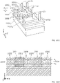
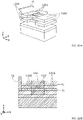
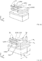
- the figure 58A presents an example of such a planar transistor conventionally comprising a source 1002, a gate 250 deposited on the surface of a channel (not visible) and a drain 1006.
- This planar architecture then gave way to other types of architectures better suited to the performance specified in technology nodes below 12 nm.
- the so-called "finFET" architecture presented at the figure 58B makes it possible, for example, to meet the performance levels set by the 7 nm technological node.
- This finFET architecture typically comprises a source 1002, a gate 250 partially encasing the channel (not visible) and a drain 1006. Gate confinement is improved here.
- this finFET architecture will have to give way to other architectures offering even improved gate confinement.
- This architecture comprises wrap-gate transistors called GAA transistors (acronym for Gate All Around) stacked on top of each other.
- GAA transistors wrap-gate transistors
- the GAA transistors shown in figure 58C are in the form of horizontal nanowires, the central parts of which are embedded within a gate 250. These central parts correspond to the channels of the transistors.
- the nanowires comprise peripheral parts extending on either side of the central parts. These peripheral parts are connected to the sources 1002 and drains 1006 of the GAA transistors.
- These GAA transistors can be stacked along z and rest for example on a buried oxide or BOX.
- such an architecture based on GAA transistors must comprise at least two stacked GAA transistors, or even four transistors stacked on top of each other along z.
- a method consists in transferring a first layer of transistors produced on a first wafer or wafer, onto a second wafer comprising a second layer of transistors. Molecular bonding can then be carried out so as to secure the layers together. Several successive transfer steps can be carried out so as to build a stack of several GAA transistors. Such a process is nevertheless complex to implement. The management of the thermal budget associated with the bonding of the layers is an important problem of this process.
- Another solution making it possible to limit the thermal budget of the transistors of the stack consists in transferring, from a first wafer of the SOI (acronym for Silicon On Insulator) type, an unstructured thin layer onto a second wafer comprising a first layer of transistors.
- SOI complementary metal-oxide-semiconductor
- the “Smart Cut” TM reference technology well known to those skilled in the art then makes it possible to separate the thin layer from the first wafer. This can then be structured so as to form a second layer of transistors by limiting the thermal budget of the transistors of the first layer.
- This method also requires several complex successive transfer steps to build a stack of several GAA transistors as illustrated in figure 58C .
- US 2019/088553 A1 , US 2010/295021 A1 and US 10 236 217 B1 disclose microelectronic devices according to the preamble of independent claim 11, each device comprising at least two vertically stacked nanowire channel transistors, the source and drain of a transistor of which are located only at its channel, and methods of manufacturing the same correspondents.
- these GAA transistors can form selection transistors of memory cells integrated according to a 3D architecture.
- a memory cell typically comprises a switchable memory element 102 associated with a selection transistor 101, as illustrated in figure 1 . Consequently, the process for manufacturing the stacked GAA transistors can be continued so as to form these memory elements. The complexity and the cost of this method of manufacturing monolithic 3D architectures increase further.
- an object of the present invention is a method of manufacturing a 3D architecture of a microelectronic device, reducing the manufacturing cost.
- Another object of the invention is a microelectronic device based on GAA transistors.
- a particular common objective of the method and of the device is to densify the GAA transistors.
- This process makes it possible to produce a stack of transistors of the GAA type (acronym for “Gate All Around”), that is to say comprising a gate completely surrounding the channel, on several levels n z . These transistors are electrically isolated from each other.
- the stack of isolated transistors is formed directly by transferring semi-conducting layers onto insulating layers, alternately. Such a transfer method is expensive and complex.
- the transistors are not isolated from each other from the start of the method. They are isolated a posteriori, during the withdrawal of the second material carried out for example via selective etching.
- the method proposed by the present invention makes it possible to considerably reduce the complexity and the cost of producing this type of transistor.
- the second material is preferably a semiconductor. It can advantageously serve as a seed layer for the epitaxy of the first material. Thus, the different layers can be formed by epitaxial growth of the first and second materials, without transfer of layers.
- the sacrificial gates advantageously make it possible to maintain the future channels of the transistors during the removal of the second material. This avoids a collapse of the transistor channels on top of each other.
- Such a method is also advantageously compatible with dense 3D integration.
- the sources and drains are advantageously formed directly by parts of the stack, before deposition or formation of the sacrificial gates in particular. This makes it possible to dispense with subsequent stages of formation of the sources and drains, for example stages of epitaxy or regrowth in solid phase of sources and drains.
- the sources of the transistors are separated from each other in the third direction z by at least one spacer, called a horizontal spacer, and/or the drains of the transistors are separated from each other in the third direction z by at least one other horizontal spacer .
- Another aspect of the invention relates to a plurality of microelectronic devices as described above.
- the invention comprises at least any one of the following optional characteristics which can be used in combination or alternatively.
- At least one of the source and the drain extends mainly in the second direction y.
- the openings are formed so that two adjacent openings define between them and in the first semiconductor material a pattern of transistors.
- the sacrificial gates are formed directly at the edge of at least one of the first and second peripheral parts.
- the method further comprises staircase etchings in a zone of source lines, so as to reach the sources of the different levels n z , and formation of contacts in a staircase on the sources of the different levels n z .
- the first semiconductor material is silicon and the second semiconductor material is a silicon-germanium alloy.
- the substrate is a semiconductor-on-insulator type substrate comprising a thin layer of semiconductor.
- the stack comprises said thin layer of semiconductor.
- said thin semiconductor layer is one of the sacrificial layer and the at least two layers made of a first semiconductor material.
- each layer of the stack has a thickness comprised between 5 nm and 50 nm, for example of the order of 15 nm.
- the removal of the at least one sacrificial layer is done by selective etching of the second semiconductor material with respect to the first semiconductor material with an etching selectivity between the second semiconductor material and the first semiconductor material greater than or equal at 5:1.
- each central part of each pattern of transistors comprises a stack of at least X channels
- each first peripheral part of each pattern of transistors comprises a stack of at least X sources
- each second peripheral part of each pattern of transistors comprises a stack of at least X drains, with X ⁇ 3 and preferably X ⁇ 4 and preferably X ⁇ 10.
- each pattern of transistors is intended to form at least X stacked transistors.
- two so-called stacked elements are not necessarily in contact with one another.
- Such is the case of the sources and the drains of each first and second peripheral part which are separated from each other successively by at least one sacrificial layer, a first space, a dielectric layer.
- the gates of the transistors are electrically connected to each other and the sources of the transistors are electrically isolated from each other. Independent sources make it possible to supply the transistors independently. This makes it possible, for example, to execute logical operations on each level independently.
- the gates of the transistors are electrically connected to each other in a word line zone of a microelectronic system of the RAM memory type (acronym for Random Access Memory).
- the sources occupying different levels n z are connected in a staircase, independently of each other, in a zone of source lines of a microelectronic system of the RAM memory type. This makes it possible to supply the transistors and/or the memory cells independently on each level of the memory cell matrix.
- the number of levels of the stack can be greater than 4, or even greater than 10.
- the number and/or the shape of the openings in the stack, the patterns of transistors illustrated in the figures can vary and be combined from way to form another mode embodiment which is not necessarily illustrated or described. Such an embodiment is obviously not excluded from the invention.
- the present invention finds as its preferred field of application the 3D integration of microelectronic systems executing logic and memory functions.
- the present invention provides in particular to produce a 3D architecture comprising a high density of nanowires superimposed on different levels.
- This 3D architecture is notably configured to electrically connect each nanowire independently.
- Each nanowire is preferably surrounded by a surrounding gate so as to obtain a GAA transistor.
- This grid is preferably bordered by longitudinal spacers. These spacers can cover the sources and the drains of the various transistors.
- the source and the drain connected to said channel extend only according to said level nz.
- the sources of the transistors are separated from each other in the third direction z by at least one horizontal spacer.
- the drains of the transistors are separated from each other in the third direction z by at least one horizontal spacer.
- the at least one horizontal spacer is made of a dielectric material.
- the sources and/or the drains are at least partly directly in contact with the gate, at the level of at least one side of the gate. This makes it possible to increase the compactness of the device. This makes it possible to densify the integration of devices in a system.
- the sources and/or the drains of different levels n z are electrically contacted with each other by at least one common contact extending in the third direction z, at the edge of said sources and/or drains.
- the sources and/or the drains of different levels n z are electrically contacted independently of each other by stepped contacts.
- a plurality of adjacent microelectronic devices along a direction of a plane normal to the third direction z form a microelectronic system in which the sources and/or the drains of a level n z of given altitude of two devices are common to said two adjacent devices.
- This increases the compactness of the system. This makes it possible to densify the integration of the devices into the system.
- a plurality of adjacent microelectronic devices along a plane comprising the third direction z form a microelectronic system in which the sources and/or the drains of a level n z of given altitude of two adjacent devices are common to said two adjacent devices.
- This increases the compactness of the system. This makes it possible to densify the integration of the devices into the system.
- the sources and/or the drains of a level n z of given altitude are separated from the sources and/or the drains of a level n z-1 and/or of a level n z+1 by at least one horizontal spacer.
- the sources and/or the drains of a level n z of given altitude extend mainly along a second direction y normal to the first and third directions x, z, and are electrically contacted with the sources and/or the drains from another level n z by a common contact located at one end in said second direction y.
- microelectronic device the manufacturing method, and the system may include, mutatis mutandis, all of the optional characteristics above.
- the term “over”, “overcomes”, “covers” or “underlying” or their equivalents do not mean “in contact with”.
- the presence of a spacer or a layer on or which covers a structural element does not necessarily mean that the spacer or that the layer are directly in contact with the structural element but this means that the spacer or that the layer at least partially covers the structural element by being either directly in contact with it, or by being separated from it ci by at least one other layer, channel, or any other element.
- two stacked elements are located at least partly in line with each other without necessarily being in contact with each other.
- a structural element is understood to mean a layer, "based" on a material A, a structural element, a layer comprising this material A only or this material A and possibly other materials, for example doping elements or elements of alloy.
- a spacer based on silicon nitride SiN can for example comprise non-stoichiometric silicon nitride (SiN), or stoichiometric silicon nitride (Si 3 N 4 ), or else a silicon oxy-nitride (SiON).
- dielectric qualifies a material whose electrical conductivity is low enough in the given application to serve as an insulator.
- a dielectric material preferably has a dielectric constant of less than 7.
- stage does not necessarily mean that the actions carried out during a stage are simultaneous or immediately successive. Certain actions of a first step can in particular be followed by actions linked to a different step, and other actions of the first step can be resumed afterwards. Thus, the term step does not necessarily mean unitary and inseparable actions in time and in the sequence of the phases of the process.
- the term "pattern of transistors" refers to the element from which the stacked transistors are formed.
- the structure of this element is in particular intended to evolve during the steps of the method.
- the transistor patterns comprise layers of a first semiconductor material and may comprise sacrificial layers and/or dielectric layers, continuous or discontinuous.
- thickness for a layer height for a device (transistor or gate for example) and depth for a cavity or an etching.
- the thickness is taken along a direction normal to the main extension plane of the layer, the height and depth are taken along a direction normal to the base plane of the substrate.
- the height and the depth are taken along the z axis of the xyz orthonormal reference frame.
- An element located directly above or plumb with another element means that these two elements are both located on the same line normal to the base plane of the substrate, i.e. on the same line oriented vertically along z in the figures.
- a direction substantially normal to a plane means a direction having an angle of 90 ⁇ 10° relative to the plane.
- the chemical compositions of the different elements or layers can be determined using the well-known EDX or X-EDS method, acronym for “energy dispersive x-ray spectroscopy” which means “energy dispersive analysis of X-ray photons”.
- This method is well suited to analyze the composition of layers or elements of small dimensions. It can be implemented on metallurgical cuts within a SEM or a TEM.
- the present invention makes it possible to manufacture a microelectronic device comprising at least two superimposed GAA type transistors. These superimposed transistors can thus be integrated into logic systems having 3D architectures. These transistors can in particular be associated with other structural or functional elements so as to design complex systems.
- the proposed method makes it possible to manufacture in a simple, reproducible and inexpensive manner a microelectronic device comprising at least two transistors and preferably at least four transistors.
- Each transistor comprises a channel in the form of a wire extending along a first direction x, a gate surrounding said channel, a source and a drain.
- the proposed method may provide for the following steps which are briefly mentioned below and which will be described in detail in the following description: Forming on a substrate a stack of alternating layers of a first semiconductor material and of a second semiconductor material. This step illustrated in figure 4A , 19 and 20 for example, will be described in detail later.
- Example 1 The steps for manufacturing a memory according to these examples are subdivided into sub-sections respectively called “formation of sacrificial gates”, “source isolation”, “structuring of the sourcelines zone”, “structuring of the wordlines zone”, “structuring of the bitlines zone”, “training of contacts”. These subsections are defined for the sake of clarity and are not necessarily strictly successive.
- the figure 2 presents a block diagram of such a resistive OxRAM memory, formed from a plurality of 10 x,y,z memory cells, each comprising a resistive element and a transistor. These 10 x,y,z memory cells are also called 1T1R cells.
- the 10 x,y,z memory cells are typically organized in a matrix fashion on different levels of integration.
- An integration level is located at an altitude z given along the Z axis.
- the memory cells 10 x,y,z are thus identified by their coordinates x and y for a given level z.
- each 10 x,y,z memory cell of this 3D matrix In order to independently address each 10 x,y,z memory cell of this 3D matrix, connecting lines are drawn. Each memory cell 10 x,y,z is thus connected to a supply or write line called sourceline SL z , a command or word line called wordline WL x , and a read or data line called bitline BL y .
- the sourcelines are carried by the levels z, the wordlines extend along Y and the bitlines extend along X.
- the resistive element is connected to a bitline BL y
- the source of the transistor is connected to a sourceline SL z
- the gate of the transistor is connected to a wordline WL x .
- the limited number of 10 x,y,z memory cells of these examples makes it possible to illustrate the main characteristics of the invention in a clear and concise manner. These examples do not exclude other possibilities for organizing the 3D matrix.
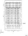
- the picture 3 presents an example of the arrangement of the structural elements of the resistive memory OxRAM.
- the 1T1R memory cells form a matrix in the XY plane at the intersection of the wordline zone 1 and the bitline zone 2.
- This arrangement may include a remote sourceline zone 3, adjoining the matrix, so as to facilitate the connection of the sourcelines .
- the structural elements of this resistive memory are mainly the transistors or selection transistors, the memory elements or memory points, and the wordlines, bitlines, sourcelines connection lines.
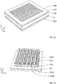
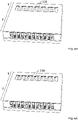
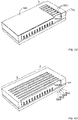
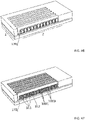
- the transistors 101 are stacked on several integration levels (along the z axis). These levels n 1 , n 2 , n 3 , n 4 notably comprise the sources 1002 of the transistors. They are electrically isolated from each other via a step of forming sacrificial gates 150. These sacrificial gates 150 are then replaced by covering functional gates, of the GAA type. This general principle makes it possible to obtain a dense 3D matrix of GAA transistors. In the examples illustrated and described below, zones of wordlines 1, bitlines 2 and sourcelines 3 are also defined and resistive memory elements 102 are formed so as to obtain a dense OxRAM memory in 3D integration.
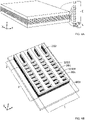
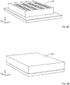
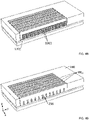
- the figures 4A and 4B illustrate stack formation and transistor pattern definition.
- the figures 4C to 4G illustrate steps for forming sacrificial gates at the transistor pattern level.
- a first step consists in producing a stack E of semiconductor layers 11, 12 on a substrate S.
- the substrate S can be a substrate of the SOI (Silicon On Insulator) type comprising, according to the terminology common to those skilled in the art , a thick layer of silicon called “Si bulk” (not shown on the figure 4A ), a silicon oxide layer called “BOX” (Burried Oxide) and a thin silicon layer called “top Si”.
- the thickness of the Si top can typically be of the order of 12 nm.
- the thickness of the BOX can typically be between 25 nm and 145 nm.
- the substrate S can be a bulk “Si bulk” substrate.
- the substrate is of the GeOI or SGOI type (respectively Germanium On Insulator or Silicon-Germanium On Insulator) known to those skilled in the art.
- the layer in contact with the BOX is a sacrificial SiGe layer. This ultimately makes it possible to form transistors all having a GAA configuration, on each level.
- Stack E typically comprises an alternation of layers 11 of silicon-germanium (SiGe) and layers 12 of silicon (Si).
- the concentration of Ge in the SiGe alloy can be 20%, 30% or 45% for example.
- This concentration of germanium is chosen so as to allow good selectivity of the etching of SiGe with respect to Si, during the steps of selective engraving.
- the greater the concentration of Ge the greater the selectivity to Si will be during the subsequent removal of SiGe.
- This stack E is advantageously formed by epitaxy of the layers of SiGe 11 and of Si 12. This step of forming the stack E is inexpensive and well known to those skilled in the art.
- the thicknesses of the Si and SiGe layers can typically be around 15 nm, and more generally between 5 nm and 50 nm for example. In a known manner, in order to avoid the formation of structural defects, the maximum thicknesses permitted for the SiGe layers 11 depend in particular on the chosen Ge concentration.
- Si the topSi layer of the substrate and three epitaxial Si 12 layers
- a Si/SiGe superlattice is thus obtained.
- the number of Si and SiGe layers can of course be increased. This ultimately makes it possible to increase the number of transistors and memory cells.
- a conventional lithography/etching step is carried out in order to define transistor patterns 101M, source patterns 301S and openings 201, 202.
- the etching is anisotropic. It is configured to burn the Si/SiGe superlattice over its entire height, stopping on the BOX. It can be carried out by plasma using an HBr/O 2 etching chemistry.
- the patterns of transistors 101M can have a length l T along X of between 100 nm and 500 nm. They preferably have a width L T along Y of between 10 nm and 80 nm, for example of the order of 40 nm. This makes it possible to obtain a plurality of superimposed Si nanowires intended to form the channels of the transistors.
- the openings 202 in the sourcelines 3 zone are significantly wider than the openings 201 of the matrix defined by the wordlines 1 and bitlines 2 zones. stepped sourceline contacts.
- the figures 4C and 4D respectively illustrate steps for depositing a layer 14 of silicon oxide SiO 2 and a layer 15 of polycrystalline silicon (polySi).
- the SiO 2 is preferably a stoichiometric oxide deposited by CVD, called TEOS from the name of the silicon precursor (TetraEthyl OrthoSilicate) generally used. This deposit is compliant.
- the thickness of SiO 2 deposited can typically be a few nanometers, for example 7 nm.
- the polySi is deposited so as to fill the openings 201, 202.
- the thickness of polySi deposited can typically be a few hundred nanometers, for example 380 nm.
- this stack makes it possible to form pseudo-grids called sacrificial grids in this application.
- These sacrificial gates are in fact kept during intermediate stages of manufacture of the devices, then removed to be finally replaced by functional gates.
- the polySi can be replaced by an amorphous silicon.
- the Figure 4E illustrates a planarization step, typically by chemical mechanical polishing CMP, configured to be stopped on the hard mask 13.
- Another hard mask 16 can then be deposited over the entire surface of the wafer, covering the hard mask 13 and the polySi exposed after planarization (not shown).
- This hard mask 16 comprises for example a layer of silicon nitride SiN with a thickness of approximately 90 nm surmounted by a layer of silicon oxide with a thickness of approximately 36 nm.
- the hard mask 16 is structured by lithography/etching so as to define the sacrificial gates.
- the sacrificial gates 150 are formed between the peripheral portions, by anisotropic etching of the polySi outside the areas covered by the hard mask 16, as illustrated in figure 4F .
- the anisotropic etching of the polySi along Z can be carried out by plasma in CH 2 F 2 SF 6 N 2 He and/or HBr/O 2 /He chemistry.
- TEOS Layer 14 and the buried oxide (BOX) advantageously serves as a stop layer during this etching of the Poly-Si.
- the sacrificial gates 150 of dimension l along X are thus formed in the “bitline” 2 and “sourceline” 3 zones. In the bitline zone 2, the sacrificial gates 150 extend between the transistor patterns. They border on either side, along Y, the peripheral portions located at each end of the transistor patterns. In the sourceline zone 3, the sacrificial gates 150 extend continuously along Y.
- the figure 4G illustrates the removal of the layer 14 of TEOS oxide, after etching of the polySi. This removal makes it possible to expose a central portion 111 of the transistor patterns, between the peripheral portions 112.
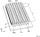
- the figure 5 illustrates the bitline zone 2 in which the central portions 111 of the exposed transistor patterns are located, and the sourceline zone 3 in which the openings 202 are bordered by the sacrificial gates 150.
- the figures 6A and 6B illustrate the formation of spacers 170, 170 c , 170 s .
- the spacers 170 c , 170 s extend mainly along y on either side of the sacrificial gates 150. These spacers 170 c , 170 s are said to be longitudinal.
- the spacers 170 extend mainly along x on either side of the transistor patterns 101M. These spacers 170 are said to be transverse.
- the spacers 170, 170 c , 170 s are typically formed from a deposit of a layer 17 of SiN ( Figure 6A ) consistent followed by anisotropic etching of this layer 17 of SiN ( figure 6B ).
- the thickness e of the SiN layer can be between 10 nm and 50 nm, for example of the order of 20 nm.
- the spacers 170 c , 170 s have a width along X equal to e and cover the sides of the hard mask 16.
- the source patterns 301S are thus partly covered by these spacers 170 s on their sides bordering the hard masks 16.
- the spacers 170 s form on the sides of the source patterns 301S an extra thickness of SiN aimed at protecting the Si/SiGe stack during subsequent etching.
- the spacers 170 c cover the peripheral portions 112 of transistor patterns 101M.
- the spacers 170 cover the sides of the central portions 111 of transistor patterns 101M.
- the parts of the SiN layer extending in planes parallel to the base plane XY, between the transverse spacers, are then opened by a first anisotropic etching, for example by plasma using a chemistry fluorocarbon, for example based on CH 2 F 2 O 2 or CH 3 F/O 2 and CHF 3 .
- a first anisotropic etching is known to those skilled in the art.
- the Si/SiGe stack underlying the open parts is then etched over its entire height, with a stop on the buried oxide layer (BOX), by a second anisotropic etching, for example by plasma using HBr/O chemistry 2 .
- the Fig. 6C illustrates the structure obtained after these first and second anisotropic etchings.
- the source patterns 301S have been partially etched and give way to openings 401 bordered by the Si/SiGe stacks surmounted by the spacers 170 s .
- the central portions 111 of the transistor patterns 101M have been etched and give way to openings 301 bordered by the spacers 170, 170c .
- These openings 301 opening onto the peripheral portions of the transistor patterns are advantageously delimited by the spacers 170, 170 c . This makes it possible to relax the constraints of resolution in lithography to subsequently fill these openings 301.
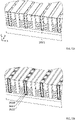
- the Figure 7A shows a transverse section passing through openings 201, along the line AA' materialized on the Fig. 6C .
- This transverse section is similar to a transverse section passing through openings 401 (not illustrated).
- the sacrificial grids 150 form a series of pillars allowing lateral anchoring of the Si/SiGe multilayers thus structured in a “comb”.
- the peripheral portions 312 of the source patterns 301S are continuous along the Y axis. A first side of these peripheral portions 312 leads to the openings 401. A second side of these peripheral portions 312 is attached to the sacrificial gates 150.
- the Si layers of these peripheral portions 312 will subsequently form the sources of the transistors.
- the figure 7B shows a transverse section passing through openings 301, along the line BB' materialized on the Fig. 6C .
- the teeth of the “comb” correspond to the peripheral portions 112 of the patterns of transistors 101M, of length l along X.
- the Si layers of these peripheral portions 112 will subsequently form the channels and the drains of the transistors.
- transistors of the 3D matrix In order to be able to independently address each of the transistors of the 3D matrix, it is necessary to at least partially isolate the transistors from one another.
- These transistors are formed from the Si layers of the Si/SiGe stack.
- the SiGe layers are therefore preferably removed and replaced by electrically insulating layers.
- the SiGe layers are said to be sacrificial. They are used to form the stack and then removed to isolate the transistors, and in particular the sources of these transistors.
- a step of isolating the sources supplying the channels of the transistors is carried out.
- These sources are formed from the Si layers of the peripheral portions 312 of the source patterns 301S illustrated in Figures 7A, 7B .
- portions of the SiGe layers of the stack are etched from the openings 301, 401.
- This etching is selective with respect to silicon, and is preferably isotropic.
- An etching solution based on acetic acid, hydrofluoric acid HF and hydrogen peroxide H 2 O 2 can be used.
- the etching is configured so that the SiGe layers of the peripheral portions 312 are etched through the openings 401.
- the etching front from the openings 401 thus stops substantially plumb with the sacrificial gates 150.
- the sources 1002 are therefore suspended.
- the etching of the SiGe layers is preferably also carried out through the openings 301.
- the selective etching of the SiGe layers is thus carried out on either side of the stack, at the level of the transistor patterns, as illustrated in figure 8A .
- Parts 113 of SiGe layers of the peripheral portions 112 are thus etched. These parts 113 form a first space which will subsequently be filled with a dielectric material.
- the etching is preferably stopped at the time before the SiGe layers are completely removed. Portions 1003 of SiGe are thus preserved.
- the peripheral portions 112 are thus subdivided into parts 112a, 112b.
- the parts 112a comprise the future channels 1001 in Si alternated with the portions 1003 in SiGe.
- the parts 112b comprise the future suspended Si drains 1006 .
- the definition of the drains 1006 and the channels 1001 can thus be done during this etching step part of the SiGe. This partial etching also makes it possible to avoid a risk of the transistor channels 1001 collapsing.
- Poly-Si sacrificial gates are used in particular to maintain the Si layers during SiGe etching. They form a structure of hanging pillars for the Si layers.
- the figure 8B illustrates the deposition of a dielectric layer 18, for example SiN, intended to fill the cavities formed by the removal of the SiGe.
- the sources 1002 are thus electrically isolated from each other.
- Layer 18 is then partially etched, for example using a solution of dilute H 3 PO 4 phosphoric acid or acetic acid or hydrogen peroxide H 2 O 2 , so as to expose the substantially parallel flanks to the YZ plane of the Si layers, on the side of the openings 401 and on the side of the openings 301.
- the BOX is preferably also exposed during this etching of the layer 18, as illustrated in Fig. 8C .
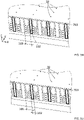
- the figures 8A to 8C illustrate these steps of removing the SiGe and isolating the sources according to a transverse section passing through the openings 301.
- the figure 8D illustrates the state of the structure after these steps of removing the SiGe and isolating the sources according to a transverse section passing through the openings 201. It clearly appears that the sacrificial gates 150 serve as a support for the sources 1002.
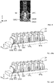
- the figure 9 is a scanning transmission electron microscopy (STEM) image illustrating a device obtained after isolation of sources 1002, as shown schematically in Fig. 8C .
- STEM scanning transmission electron microscopy
- the remaining portions of SiGe 1003 are visible between the channels 1001 of the transistors.
- the plugs 1004 formed by the deposition of the SiN layer 18 are also visible on either side of the SiGe portions 1003.
- the protective layer 50 is an epitaxy produced for other needs.
- the figures 10A and 10B present enlargements of the structure obtained respectively before and after insulation.
- the figure 10A illustrates in an enlarged way a transverse section according to the line CC' represented on the Figure 7A , passing through the openings 401 of the sourceline zone.
- the figure 10B illustrates in an enlarged way a transverse section according to the line DD' represented on the figure 8D , passing through the openings 401 of the sourceline zone.
- Sacrificial gates 150, spacers 170 c , 170 s , hard masks 13 and 16, and sources 1002 are visible on both Figures 10A, 10B .
- the SiGe portions 1005 of the peripheral portions 312 of the source patterns 301S present before isolation ( figure 10A ) are replaced by the SiN plugs 1004 in the peripheral portions 312 of the source patterns 301S after isolation ( figure 10B ).
- the openings 401, 301, 201 between the hard mask lines 16 are preferably filled with a TEOS 180 oxide.
- the structure is then planarized by CMP until the hard mask 16 is removed, so as to expose the hard mask 13.
- this hard mask 13 can then be removed in the sourceline zone 3, so as to expose the polySi of the sacrificial gates 150, as illustrated in figure 11A .
- the hard mask 13 SiN can be etched using a solution of dilute H 3 PO 4 phosphoric acid, or by dry plasma etching based on fuorocarbon species (for example CH 2 F 2 /O 2 ).
- the sacrificial grids 150 of the sourceline zone 3 are then removed, as illustrated in figure 11B .
- the polySi of the sacrificial gates can be etched using a solution of tetramethylammonium hydroxide (TMAH) or tetraethylammonium hydroxide (TEAH).
- TMAH tetramethylammonium hydroxide
- TEAH tetraethylammonium hydroxide
- the TEOS oxide of the sacrificial gates can be etched using a plasma in fluorocarbon chemistry, for example in CF 4 / CH 2 F 2 / He chemistry.
- the withdrawal of the sacrificial gates 150 forms openings 501.
- These openings 501 expose the second side of the peripheral portions 312 comprising the stack of sources 1002 isolated from each other by the SiN plugs 1004.
- the sacrificial gates have thus made it possible to form a support to the sources 1002 during the replacement of the SiGe portions 1005 by the SiN plugs 1004 in the peripheral portions 312.
- this replacement can be done in a single step such as previously illustrated by figures 7A to 8D .
- the SiGe 1005 portions have a width along X greater than 100 nm, for example 150 nm or 200 nm, the complete removal of these portions 1005 can cause the sources 1002 to collapse or stick together.
- a partial removal of the portions 1005 over a width along X less than 100 nm can first be performed from the openings 401 emerging on the first side of the peripheral portions 312 (not shown). Then, after removal of the sacrificial gates, a further removal of the portions 1005 over a remaining width along X can be performed from the openings 501 leading to the second side of the peripheral portions 312.
- the sacrificial gates first form a support during the first partial removal of the SiGe interposed between the sources, then, by removing them, these sacrificial gates allow access for the second additional removal of the SiGe interposed between the sources.
- This replacement in two stages by means of sacrificial gates makes it possible, for example, to size the sources so that they have a width of between 1 time and 2 times the critical collapse width of the sources, ie the width above beyond which springs are likely to collapse.
- the openings 501 are preferably filled with a deposit of SiN 160. This deposit is followed by planarization by CMP with a stop on the TEOS 180 oxide layer, as illustrated to the figure 11D .
- Sources 1002 are thus completely isolated from each other in sourceline 3 zones.
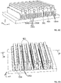
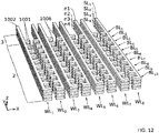
- the figure 12 shows only the Si-based elements of the structure.
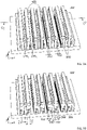
- This silicon "skeleton" can in particular make it possible to form a 3D matrix comprising 8 wordlines WL 1 , WL 2 , WL 3 , WL 4 , WL 5 , WL 6 , WL 7 , WL 8 , 4 levels n1, n2, n3, n4 of sourcelines SL 1 , SL 2 , SL 3 , SL 4 and 10 bitlines BL 1 , BL 2 , BL 3 , BL 4 , BL 5 , BL 6 , BL 7 , BL 8 , BL 9 , BL 10 .
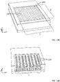
- the Figure 13A illustrates a masking, for example by lithography, making it possible to protect the sourceline zone 3 while exposing the wordlines zone 1.
- the WLs are carried out at the level of the hard mask lines 13.
- an etching of the hard mask 13 is carried out so as to expose the polySi of the sacrificial gates 150 of the wordlines zone 1.
- This etching of the hard mask 13 in SiN can be done by plasma, for example using a chemistry of plasma CH 2 F 2 /O 2 or CHF 3 /He and CH 3 F/O 2 /He/CH 4 .
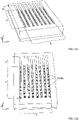
- the sacrificial grids 150 of the wordlines zone 1 are then removed, as illustrated in Figures 13C, 13D .
- the polySi of the sacrificial grids can be etched using a solution of tetramethylammonium hydroxide (TMAH) or tetraethylammonium hydroxide (TEAH) ( figure 13C ).
- TMAH tetramethylammonium hydroxide
- TEAH tetraethylammonium hydroxide
- the TEOS oxide of the sacrificial gates can be etched using a plasma in fluorocarbon chemistry, for example in CF 4 / CH 2 F 2 / He chemistry ( figure 13D ).
- openings 511 are bordered by two peripheral portions 112 of patterns of transistors 101M, a first side of peripheral portions 312 comprising the stack of sources 1002 isolated from each other, and a spacer 170 c (not visible).
- the peripheral portions 112 of patterns of transistors 101M here each comprise a part 112a formed of a stack of Si nanowires between which there are portions 1003 of SiGe, and a part 112b formed of a stack of Si nanowires between which find 1004 SiN plugs.
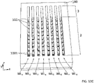
- the Figure 13E illustrates the selective etching of portions 1003 of SiGe. This makes it possible to form a second space which will then be filled in to form a functional grid.
- This etching has good selectivity S SiGe:Si relative to Si, preferably S SiGe:Si > 5:1. This makes it possible to etch the SiGe while preserving the Si nanowires and the parts of the sources 1002 exposed at the level of the first side of the peripheral portions 312.
- This etching also has good selectivity S SiGe:SiN with respect to SiN, preferably S SiGe: SiN > 5:1. This makes it possible to etch the SiGe while preserving the SiN spacers 170 c and the plugs 1004. The etching is thus confined along the WLs, being stopped laterally by the SiN spacers 170 c and the first side of the peripheral portions 312.
- the Figure 13F illustrates the formation of functional grids instead of sacrificial grids.
- Successive depositions of materials used for the formation of functional gates make it possible to form the functional gates 250 around each channel 1001.
- These functional gates can be formed from a deposition of material with a high dielectric constant called high-k, for example HfO 2 over a thickness of 2 nm, followed by a deposit of TiN over a thickness of 3 nm, followed by a deposit of tungsten W aimed at filling the openings 511 and the wordlines WL x delimited by the oxide TEOS 180.
- Planarization by CMP with stop on the oxide TEOS 180 makes it possible to remove the excess metallic layers if necessary.
- the transistors of the 3D array are therefore gate-all-around MOS transistors based on stacked Si nanowires.
- Sources 1002 extend along Y as far as sourceline zone 3.
- Drains 1006 extend along X as far as opening zones 301 filled with oxide 180.
- the next step consists in removing the oxide 180 from the areas of openings 301, so as to gain access to the drains 1006 of the transistors.
- the Figure 14A illustrates a lithography step prior to the etching of the oxide 180 at the level of the opening zones 301.
- the alignment constraints linked to this lithography step are reduced thanks to the presence of the spacers 170 embedded in the oxide 180.
- a selective etching of the oxide 180 with respect to the SiN nitride of the spacers 170 therefore makes it possible to "automatically” expose the openings 301 leading to the drains 1006, as illustrated in Figure 14B .
- the subsequent formation of the resistive elements of the memory points precisely at the level of the openings 301 is thus advantageously assisted by the presence of the spacers 170 defining the openings 301.
- This step of lithography/etching of the oxide 180 intended to opening the memory dot areas is said to be “self-aligned”, due to the presence of spacers 170 guiding the etching of oxide 180.
- the openings 301 are filled by successive depositions so as to form the memory elements or memory points 102, as illustrated in figure 14C and 15 , respectively according to a transverse section and a longitudinal section.
- these memory points can be based on HfO 2 .
- these memory points can be made by depositing an HfO 2 1021 layer, for example 5 nm thick, followed by depositing a Ti 1022 layer, for example 5 nm thick, followed by a deposition of a layer of TiN 1023, for example with a thickness greater than 5 nm followed by deposition of a layer of W 1024, for example with a thickness of 300 nm.
- the layer of W 1024 can typically extend outside the openings 301. It is then planarized by CMP with a stop on the layer of oxide 180.
- the memory points 102 thus formed are directly in contact with the drains 1006 of the selection transistors.
- the drains 1006 can be silicided beforehand before the deposition of the layers forming the memory elements 102.
- the self-alignment of the memory points with the drains 1006 of the selection transistors makes it possible in particular to bring these two elements together forming a resistive memory cell . This makes it possible to increase the density of resistive memory cells within the 3D matrix.
- each memory element 102 has an edge or flank in contact with an edge or flank of a spacer 170 c surmounting the stack forming the drains of the transistors.
- edges or flanks extend mainly along planes parallel to the plane yz.
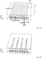
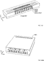
- the figure 16A illustrates a lithography step aimed at forming contacts in the sourceline zone 3 of the 3D matrix.
- the contacts to be formed in the sourceline zone 3 are preferably stepped contacts.
- a sequence of lithography/etching steps then makes it possible, in a known manner, to form such contacts in a staircase, on each of the source levels.
- a first line 601 of contact patterns is defined by lithography ( figure 16A ).
- a first burn configured to reach and burn the first source level n1 is then performed ( Figure 16B ).
- a second lithograph can then make it possible to define a second line 602 of contact patterns, while keeping the first line 601 exposed.
- a second etching similar to the first etching is performed. This makes it possible to simultaneously reach and burn the first source level n 1 at the level of the second line 602 and the second source level n 2 at the level of the first line 601 ( Fig. 16C ).
- a third lithograph can then make it possible to define a third row 603 of contact patterns, while keeping the first and second rows 601, 602 exposed.
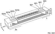
- a third etching similar to the first and second etchings is performed. This makes it possible to simultaneously reach and burn the first source level n 1 at the level of the third line 603, the second source level n 2 at the level of the second line 602 and the third source level n 3 at the level of the first line 601 ( figure 16D ).
- n 4 In the example illustrated here comprising 4 source levels n 1 , n 2 , n 3 , a fourth and last lithography/etching makes it possible to reach and expose the first source level n 1 at the level of a fourth line 604 ( figure 16D ).
- the 4 levels of sources n 1 , n 2 , n 3 , n 4 are thus respectively exposed in staircase at the level of lines 604, 603, 602, 601. This makes it possible to then form contacts in staircase making it possible to independently connect the various levels of sources.
- Source levels n 1 , n 2 , n 3 , n 4 can be exposed via lines 604, 603, 602, 601 in the sourceline 3 area, and possibly via lines 604b, 603b, 602b, 601b in another area sourceline 3b as shown on the figures 16B to 16D .
- the dimension reduction of the resin used during the lithography/etching can advantageously be used to reduce the number of lithography steps.
- nitride 701 with a thickness of between 5 nm and 20 nm, for example approximately 10 nm, is deposited in the sourceline zones 3, 3b.
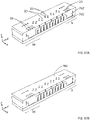
- a thick 702 SiO2 oxide layer is then deposited on the entire structure and planarized by CMP, as shown in figure 17A .
- the contact holes 31, 32, 33 are then formed by lithography/etching through the oxide layer 702 ( figure 17A ).
- the contact holes 31 are dedicated to the connection of the wordlines with the gates of the selection transistors.
- the contact holes 32 are dedicated to the connection of the bitlines with the memory points.
- the contact holes 33 are dedicated to the connection of the source lines with the sources of the selection transistors.
- the nitride layer 701 serves as a stop layer for etching the contact holes 33 in the sourceline zones 3, 3b.
- the tungsten layers of the functional gates and of the memory points serve as a stop layer for the etching of the contact holes 31, 32.
- the nitride layer 701 is then etched at the level of the contact holes 33 to expose the silicon of the sources.
- the contacts are then formed by filling the contact holes 31, 32, 33 by successive deposits of TiN with a thickness of approximately 7 nm and of tungsten W with a thickness of approximately 200 nm. Planarization by CMP with stoppage on the oxide layer 702 makes it possible to obtain a 3D matrix of integrable memory cells, as illustrated in figure 17B .
- the figure 18 shows such a 3D array of memory cells without layer 702, for clarity.
- Sourceline contact lines SL1, SL2, SL3, SL4, wordlines WL 1 , WL 2 , WL 3 , WL 4 , WL 5 , WL 6 , WL 7 , WL 8 and bitline BL 1 , BL 2 , BL 3 , BL 4 , BL 5 , BL 6 , BL 7 , BL 8 , BLg, BL 10 are also visible in transparency on this figure 18 .
- the contacts 31, 33 illustrated here correspond to another possibility of integration of the 3D matrix, slightly different from that illustrated by the Figures 17A, 17B . Obviously, these contacts can be defined according to different organizational plans, depending on the integration constraints.
- a second embodiment of a resistive memory of the OxRAM type will now be described with reference to the figures 19 to 57 in the next section. Only the distinct characteristics of the first exemplary embodiment are described in detail below, the other characteristics not described or partially described being deemed to be substantially identical to those of the first exemplary embodiment.
- a thin layer of SiO 2 oxide denoted BOX, and a thin layer of Si denoted topSi thin layers of SiGe 11 and of Si 12 are alternately formed by epitaxy .
- the figure 19 only illustrates the BULK and BOX of the SOI substrate.
- the figure 20 illustrates the Si/SiGe superlattice denoted R comprising the topSi and the alternating SiGe 11 and Si 12 layers.
- the figure 21 illustrates a lithography step aimed at defining the various sourcelines, wordlines, bitlines zones by a first mask 13B.
- the figure 22 illustrates the anisotropic etching along Z of the stack E with a stop on the BOX. It can be carried out as before by plasma using an HBr/O 2 etching chemistry.
- the openings 202 in the sourcelines 3 zone are significantly wider than the openings 201 of the matrix defined by the wordlines 1 and bitlines 2 zones. This makes it possible to reserve slots wide enough for the formation of the sourceline contacts, in particular for the stepped sourceline contacts.
- the formation of the staircase contacts is carried out before the other steps.
- the figure 23 illustrates a lithography step aimed at forming contacts in the sourceline zone 3 of the 3D matrix.
- the contacts to be formed in the sourceline zone 3 are preferably stepped contacts.
- a sequence of lithography/etching steps then makes it possible, in a known manner, to form such contacts in a staircase, on each of the source levels.
- a deposition of resin 61 is first carried out so as to cover all of the sourceline 3, wordlines 1 and bitlines 2 zones previously structured. This helps protect areas outside of the area of interest for the formation of staircase contacts.
- a first opening in the sourceline zone 3 making it possible to expose the SiGe layer 11 1 relative to the level n 1 , at the level of the lines 601, 602, 603 of contact patterns, is defined by lithography ( figure 23 ).
- a first etching configured to reach and etch the first level n1 of Si is then performed ( figure 24 ).
- a second lithography (FIG. 25) can then define a second opening making it possible to expose the SiGe layer 11 2 relating to level n 2 , at the level of lines 601, 602, of contact patterns.
- a second etching similar to the first etching is performed. This makes it possible to reach and burn the second level n 2 of Si at the level of lines 601, 602 ( figure 26 ).
- a third lithography (FIG. 27) can then define a third opening making it possible to expose the SiGe layer 11 3 relating to level n 3 , at the level of line 601, of contact patterns.
- a third etching similar to the first and second etchings is performed. This makes it possible to reach and engrave the third level n 3 of Si at line 601 ( figure 28 ).
- the SiGe layers 11 1 , 11 2 , 11 3 , 11 4 are exposed in a staircase respectively at the level of lines 604, 603, 602, 601 from sourcelines area 3 ( figure 28 ).
- a lithography/etching step is advantageously eliminated in this second exemplary embodiment, compared to the first exemplary embodiment.
- Resin 61 is not necessarily completely removed and/or redeposited between each lithography/etching.
- the figures 29 to 33 illustrate steps in the formation of the sacrificial grids.
- the figures 29 and 30 respectively illustrate steps for depositing a layer 14 of silicon oxide SiO 2 and a layer 15 of polycrystalline silicon (polySi).
- the thickness of SiO 2 deposited can typically be a few nanometers, for example 7 nm.
- the polySi is deposited so as to fill the openings 201, 202.
- the thickness of polySi deposited can typically be a few hundred nanometers, for example 380 nm.
- the figure 31A illustrates a polySi 15 planarization step, typically by CMP chemical mechanical polishing. This CMP can be stopped on time, for example after a few tens of seconds.
- the patterns 101M, 301S of the wordlines and bitlines zones, as well as the staircase-structured contacts of the sourcelines zone are visible by transparency through the planarized polySi layer 15.
- the figure 31B is a cross-sectional view along XZ through patterns 101M, of the structure obtained at the end of the step illustrated in figure 31A .
- the 101M patterns of length l T and width LT, formed in the superlattice R, are visible on this figure 31B .
- the figure 32 illustrates a lithography step aimed at defining the sacrificial gates via a second mask 16B.
- a layer of nitride 13B and a layer of SiO 2 oxide 13C are successively deposited on the planarized polySi layer 15 .
- the figure 33 illustrates the anisotropic etching along Z of the oxide 13C, of the nitride 13B and of the polySi 15.
- the layer 14 of TEOS and the buried oxide (BOX) advantageously serve as a stop layer during the etching of the Poly-Si.
- the sacrificial gates 150 are thus formed astride the peripheral portions of the transistor patterns 101M. They extend mainly along Y and border along X the source patterns 301S, as before.
- the figure 34 illustrates the formation of spacers 170 c , 170 s on either side of the sacrificial gates 150. These spacers are typically formed from the deposition of a conformal SiN layer followed by anisotropic etching of this layer of SiN, as before.
- the source patterns 301S are thus partly covered by the spacers 170 s .
- the transistor patterns 101M are thus partly covered by the spacers 170 c .
- the figure 35 illustrates the removal of the exposed parts of the layer 14 of TEOS oxide, after formation of the spacers 170 c , 170 s .
- This withdrawal makes it possible to expose a central portion 111 of the transistor patterns 101M, between the spacers 170 c , and a central portion 311 of the source patterns 301 S between the spacers 170 s .
- central portions 111 and 311 are then etched anisotropically along Z, up to the BOX, as illustrated in figure 36 . This makes it possible to structure the Si/SiGe stack in the form of a comb.
- Peripheral portions 312 of source patterns 301S are retained after this etching, under spacers 170 s . These peripheral portions 312 are continuous along the Y axis. They form the body of the comb. A first side of these peripheral portions 312 leads to the openings 401. A second side of these peripheral portions 312 is attached to the sacrificial gates 150. Preferably, the Si layers of these peripheral portions 312 will subsequently form the sources of the transistors.
- Peripheral portions 112 of transistor patterns 101M are also retained after this etching, under sacrificial gates 150 and spacers 170 c . These peripheral portions 112 extend along X and lead to the openings 301c. The peripheral portions 112 form the teeth of the comb. They are interconnected by the peripheral portions 312. Preferably, the Si layers of these peripheral portions 112 will subsequently form the channels and the drains of the transistors.
- the sources 1002 of the transistors correspond to the Si layers of the peripheral portions 312 of the source patterns 301S. To isolate these sources 1002 from each other, portions of the SiGe layers of the stack are etched from the openings 401, 301c, as before.
- the etching is configured in such a way that the SiGe layers of the peripheral portions 312 are etched through the openings 401.
- the stopping of the etching front can be time-controlled, preferably substantially plumb with the sacrificial gates 150. sources 1002 are therefore suspended.
- the etching of the SiGe layers preferably also takes place through the openings 301c.
- the selective etching of the SiGe layers is thus done by and on the other side of the stack, at the level of the transistor patterns, as illustrated in figure 37 .
- Parts 1006 of the Si layers of the peripheral portions 112b of the transistor patterns 101M are therefore suspended. These parts 1006 are in the form of wires and correspond substantially to the drains of the transistors.
- the etching is preferably stopped before the SiGe layers are completely removed. Portions 1003 of SiGe are thus kept between the Si layers of the peripheral portions 112a of the patterns of transistors 101M. This makes it possible both to define the channels 1001 and/or the drains 1006 in Si, and to avoid a risk of the Si layers collapsing. These portions 1003 are subsequently removed so as to form the surrounding gates of the GAA transistors .
- Poly-Si sacrificial gates are used in particular to maintain the Si layers during SiGe etching. They form a structure of hanging pillars for the Si layers.
- the figure 38 illustrates the formation of dielectric plugs 1004, for example made of SiN, at the level of the cavities formed by the removal of the SiGe, as previously.
- the sources 1002 are thus electrically isolated from each other.
- the drains 1006 are also electrically isolated from each other.
- An oxide layer 180 is then deposited so as to fill the openings 401, 301c ( figure 38 ). This layer of oxide 180 is then planarized by CMP with stop on the parts 13B of hard mask in SiN, as illustrated in the figure 39 .
- a lithography step is carried out in order to protect the bitlines zone 2 and to expose the sourcelines zone 3 ( figure 40 ).
- the hard mask 13B is removed in this sourcelines zone 3, so as to expose the sacrificial gates 150 at the level of the sourcelines zone 3 ( figure 41 ).
- the sacrificial grids 150 of the sourceline zone 3 are then removed, as illustrated in figure 42 .
- the polySi of the sacrificial gates can be etched using a TMAH or TEAH solution, or by anisotropic plasma etching, for example based on CH 2 F 2 /SF 6 /N 2 /He and HBr/O 2 / Hey, as before.
- the withdrawal of the sacrificial grids 150 forms openings 501. These openings 501 lead to the stepped contacts connected at sources 1002 (not visible).
- the openings 501 are bordered by the spacers 170 c , 170 s .
- the resin 61 is then removed so as to expose the bitline zone 2.
- the nitride of the hard mask 13B in the bitline zone 2 and of the spacers 170 c , 170 s in the sourceline zone 3 is then etched, as illustrated in figure 43 .
- the lines 604, 603, 602, 601 of contact patterns, each corresponding to a step of the contacts in a staircase, are also represented. to the figure 43 .
- a thick 702 SiO 2 oxide layer is then deposited on the entire structure ( figure 44 ) and planarized by CMP with stop on the vertices of the sacrificial grids 150 ( figure 45 ).
- the figures 46 and 47 illustrate the removal of the sacrificial grids 150 from the wordlines zone 1, as before.
- the polySi ( figure 46 ) then the TEOS ( figure 47 ) are successively removed.
- the withdrawal of the sacrificial gates 150 forms openings 511.
- These openings 511 are bordered along XZ by stacks formed by the Si channels 1001 and the SiGe portions 1003.
- These openings 511 are bordered along YZ by the peripheral portions 312 comprising the stack sources 1002 isolated from each other, and by the spacers 170 c (not visible) facing said peripheral portions 312.
- the figure 48 illustrates the selective etching of portions 1003 of SiGe, as before. This etching makes it possible to etch the SiGe while preserving the channels 1001 in the form of Si nanowires and the parts of the sources 1002 exposed at the level of the peripheral portions 312. At the end of the etching, the channels 1001 of the Si transistors are suspended between the openings 511 of a same wordline WL x .
- the figure 49 illustrates the formation of functional grids instead of sacrificial grids.
- Successive deposits of materials used for the formation of functional gates make it possible to form the functional gates 250 around each channel 1001, as previously.
- These functional gates can be formed from a deposit of high dielectric constant material called high-k, for example HfO 2 over a thickness of 2 nm, followed by a deposit of TiN over a thickness of 3 nm, followed by a deposit of tungsten W aimed at filling the openings 511 and the wordlines WL x delimited by the TEOS 180 oxide. Planarization by CMP with a stop on the TEOS 180 oxide allows the excess metal layers to be removed if necessary.
- the WL x wordlines are thus defined.
- the transistors of the 3D array are gate-all-around MOS transistors based on stacked Si nanowires.
- the figure 50 makes it possible to distinguish in cross-section along XZ the sources 1002 of the transistors, the channels 1001 surrounded by the surrounding gates 250, and parts of nanowire forming the drains 1006 of the transistors.
- Sources 1002 extend along Y as far as sourceline zone 3.
- Drains 1006 extend along X as far as opening zones 301c filled with oxide 180.
- the next step consists in partially removing the oxide 180 from the opening zones 301c, so as to access the drains 1006 of the transistors in the bitline zone 2.
- the figure 50 illustrates a lithography step prior to the etching of the oxide 180 at the level of the opening zones 301c.
- the selective etching of the oxide 180 makes it possible to form openings 301B exposing one end of the drains 1006 in Si, as illustrated in figure 51 .
- These openings 301B are filled by successive deposits so as to form the memory points, as illustrated in figures 52 and 53 .
- the memory points thus formed are directly in contact with the drains 1006 of the selection transistors.
- 1006 drains can be silicided beforehand.
- these memory points can be based on HfO 2 .
- these memory points can be made by depositing an HfO 2 layer 1021 with a thickness of 5 nm, followed by a deposit of a layer of Ti 1022 with a thickness of 5 nm, followed by a deposit of a layer of TiN 1023 with a thickness greater than 5 nm followed by the deposition of a layer of W 1024 with a thickness of 300 nm.
- W layer 1024 may typically extend outside of openings 301c. It is then planarized by CMP with a stop on the oxide layer 180.
- An oxide layer 703 is preferably deposited on the 3D matrix thus formed.
- the contact holes 32 are then formed by lithography/etching through the oxide layer 703, as shown in figures 54 and 55 .
- the contact holes 32 are dedicated to the connection of the bitlines with the memory points.
- the contact holes dedicated to the connection of the wordlines with the gates of the selection transistors and the contact holes 33 dedicated to the connection of the sourcelines with the sources of the selection transistors are also formed by lithography/etching through the oxide layers 703, 702.
- the figure 56 and 57 present a 3D resistive memory obtained by this second embodiment, respectively according to a transverse section along XZ and according to a longitudinal section along YZ.
- the sourceline contact lines SL1, SL2, SL3, SL4 independently connecting each of the levels n 1 , n 2 , n 3 , n 4 of the matrix, the wordlines WL1, WL2, WL3, WL4, WL5, WL6, WL7, WL8, WL9, WL10, WL11, WL12 and bitlines BL1, BL2, BL3, BL4, BL5, BL6, BL7, BL8, BL9, BL10 are visible in transparency on these figure 56 and 57 . Contacts 32, 33 are also shown on these figure 56 and 57 .
- the present invention also relates to a microelectronic device comprising at least two transistors stacked according to z.
- Each of these transistors comprises a channel in the form of a wire extending mainly along the first direction x, a gate surrounding said channel, a source and a drain.
- the length of each channel extends along the first direction x.
- a level n z of given altitude corresponds to a portion of space delimited by two planes P1n z , P2n z perpendicular to the third direction z and passing respectively through an upper face 251n z of the channel of the transistor associated with level n z , and a lower face 252n z of the channel of the transistor associated with level n z .
- Source 1002 and drain 1006 connected to said channel are entirely contained in this portion of space.
- two levels n z of different altitudes are separated from each other by a so-called horizontal spacer, preferably made of a dielectric material.
- two levels n z of given altitude is meant two levels having two different altitudes.
- Such a device is advantageously manufactured by the process according to the invention.
- the plugs formed in the manufacturing process advantageously correspond to the horizontal spacers of the device.
- These devices preferably comprise at least one horizontal spacer 1004 separating the source 1002 of a level n z from the source 1002 of a level n z-1 or n z+1 adjacent to this level n z .
- these devices preferably comprise at least one horizontal spacer 1004 separating the drain 1006 of a level n z from the drain 1006 of a level n z-1 or n z+1 adjacent to this level n z .
- the source 1002 and the drain 1006 of a transistor occupying a level n z are located only on this level n z , between horizontal spacers 1004.
- a first horizontal spacer separates the levels n z and n z-1 and a second horizontal spacer separates levels n z and n z+1 .
- These first and second horizontal spacers may be separate from each other, at least along a section of the device taken along the plane zx.
- the sources S are stacked along z one above the other and form a stack S/S/S/S/S.
- the drains D can be stacked along z one above the other so as to form a stack D/D/D/D/D/D.
- Other stacks alternating the sources and the drains can also be envisaged, for example S/D/S/D/S/D or S/D/D/S/S/D.
- the sources and/or the drains of different levels n z are separated from each other by horizontal spacers.
- a zone forming a source 1002 or a drain 1006 does not extend over several levels of transistors.
- the source 1002 and/or the drain 1006 associated with the channel 1001 of a level n z of given altitude are arranged at a distance from a source and/or a drain associated with a channel of a level n z-1 or n z+1 adjacent to the level n z .
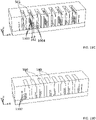
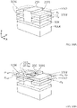
- the figures 59A to 59C show a first example of a device comprising two levels n 1 , n 2 and four transistors distributed over these two levels, for the sake of clarity.
- the number of levels illustrated is not limited to the invention. Three, four or more levels, for example ten, are perfectly possible within the scope of the invention.
- each level n 1 , n 2 comprises a source 1002 extending mainly along y and a drain 1006 extending mainly along y ( figure 59A ).
- the source and drain 1002, 1006 of level n 1 are interconnected by two channels 1001 in the form of wires extending along x.
- the source and drain 1002, 1006 of level n 2 are also interconnected by two channels 1001 in the form of wires extending along x ( figure 59B ).
- the source and drain 1002, 1006 of level n 1 are separated from the source and drain 1002, 1006 of level n 2 by plugs 1004, also called horizontal spacers. These horizontal spacers are for example made of silicon nitride or silicon dioxide. They make it possible to isolate the source and drain 1002, 1006 of a given level n z , for example n 1 , with respect to the lower levels n z+1 , for example n 2 , and/or with respect to the upper levels n z -1 .
- the enclosing grid 250 completely coats the channels 1001 and here has a first side 2501 flush with the sources 1002 and the horizontal spacers 1004, and a second side 2502 flush with the drains 1006 and the horizontal spacers 1004 ( figure 59C ).
- a first fine gate oxide can be inserted between the horizontal spacers 1004 and the first side 2501 and/or the second side 2502 (not illustrated).
- the first side 2501 of the enclosing gate 250 is preferably directly in contact with the sources 1002.
- the second side 2502 of the enclosing gate 250 is preferably directly in contact with the drains 1006.
- the source or sources 1002 of a level n z can each have a length along y, for example L1, different from the lengths along y, for example L2, of the source or sources 1002 of another level n z , for example n 2 .
- the drain(s) 1006 of a level n z can each have a length along y, for example L1, different from the lengths along y, for example L2, of the drain(s) 1006 of another level n z , for example n 2 .
- stepped contacts 33 are formed at one end of the sources 1002.
- the sources 1002 can be common to several transistors of the same level n z .
- stepped contacts 32 are formed at one end of the drains 1006.
- the drains 1006 can be common to several transistors of the same level n z .
- the drain 1006 of level n 1 is connected to four channels 1001a, 1001b, 1001c, 1001d belonging respectively to four distinct transistors of level n 1 .
- the figure 61B illustrates in section the system of the figure 61A .
- Sources 1002 and drain 1006 of level n 1 are isolated from sources 1002 and drain 1006 of level n 2 by horizontal spacers 1004.
- a contact 34 can extend over one side of the drains 1006 and/or sources 1002 (not shown) of different levels n z , so as to electrically connect said drains 1006 and/or sources 1002 in common.
- the drains 1006 extend in the form of wires along x, in extension of the channels 1001.
- vertical contacts in the form of through vias 35 can extend on one side of said drains 1006 in the form of wires, along of different levels n z .
- the drains 1006 extend in the form of wires along x, in extension of the channels 1001 and, as before, vertical contacts in the form of through vias 35 extend on one side of said drains 1006 in the form of wires, along the different levels n z .
- the sources 1002 extend mainly along y and have different lengths for different levels nz .
- source 1002 of level n 1 has a length L1 less than length L2 of source 1002 of level n 2 . This makes it possible to contact the sources 1002 by stepped contacts 33.
- the different transistors of the different levels n z can thus be controlled independently of each other.
- the invention is not limited to the embodiments described but extends to any embodiment falling within the scope of independent claims 1 and 11.
- the present invention covers methods for producing devices microelectronics that do not include memory cells.
- the drains and the sources of the transistors can be inverted, independently of each other.
Landscapes
- Engineering & Computer Science (AREA)
- Manufacturing & Machinery (AREA)
- Metal-Oxide And Bipolar Metal-Oxide Semiconductor Integrated Circuits (AREA)
- Chemical & Material Sciences (AREA)
- Nanotechnology (AREA)
- Semiconductor Memories (AREA)
- Thin Film Transistor (AREA)
Claims (15)
- Verfahren zur Herstellung einer Mikroelektronikvorrichtung, umfassend mindestens zwei Transistoren (101), jeweils umfassend einen Kanal (1001) in Drahtform, der sich hauptsächlich entlang einer ersten Richtung x erstreckt, ein Gitter (250), das den Kanal (1001) umgibt, eine Source (1002) und einen Drain (1006), assoziiert mit dem Kanal (1001), wobei die Transistoren (101) entlang einer dritten Richtung z gestapelt sind und entlang der dritten Richtung z jeweils ein gegebenes Höhenniveau nz, nz = n1...n4 einnehmen,
wobei das Verfahren die folgenden Schritte umfasst:- Bilden, auf einem Substrat, einer Stapelung (E) entlang der dritten Richtung z, umfassend mindestens zwei Schichten (12) aus einem ersten Halbleitermaterial, getrennt durch mindestens eine Opferschicht (11), und ein zweites Halbleitermaterial,- Bilden von Öffnungen (201, 202, 301, 301c, 401) ausgehend von dieser Stapelung (E), die Transistormuster (101M) definieren, wobei die Transistoren (101M) jeweils einen Mittelteil (112a), der sich insbesondere und vorzugsweise hauptsächlich entlang der ersten Richtung x erstreckt, und erste und zweite periphere Teile (312, 112b), die sich beiderseits des Mittelteils (112a) erstrecken, umfasst, wobei der Mittelteil (112a) dazu bestimmt ist, die Kanäle (1001) der Transistoren zu bilden und die ersten und zweiten peripheren Teile (312, 112b) dazu bestimmt sind, jeweils die Sourcen (1002) und die Drains (1006) der Transistoren zu bilden,- Bilden von Opfergittern (150), zum Teil in den Öffnungen (201, 202), gebietsübergreifend auf den Mittelteilen (112a) der Transistormuster (101M) und sich hauptsächlich entlang einer zweiten Richtung y senkrecht zu der ersten Richtung x erstreckend,- Entfernen, ausgehend von den Öffnungen (201, 202), des zweiten Halbleitermaterials der mindestens einen Opferschicht (11) von den Transistormustern (101M),- Füllen, durch ein zweites dielektrisches Material, eines durch die Entfernung zurückgelassenen ersten Raums auf dem Niveau der ersten und zweiten peripheren Teile (312, 112b) der Transistormuster (101M) der mindestens einen Opferschicht (11),- Entfernen der Opfergitter (150),- Füllen, durch ein Gittermaterial, eines durch die Entfernung zurückgelassenen zweiten Raums auf dem Niveau der Mittelteile (112a) der Transistormuster (101M) der mindestens einen Opferschicht (11) derart, dass die einkapselnden Gitter (250), die die Kanäle (1001) der Transistoren (101) von mindestens einem Niveau nz unter den gegebenen Höhenniveaus komplett umgeben, gebildet werden. - Verfahren nach dem vorstehenden Anspruch, wobei die Entfernung der mindestens einen Opferschicht (11) umfasst:- Eine erste Entfernung, konfiguriert, um vor der Entfernung der Opfergitter (150) den ersten Raum auf dem Niveau der ersten und zweiten peripheren Teile (312, 112b) zu bilden, und- Eine zweite Entfernung, konfiguriert, um nach der Entfernung der Opfergitter (150) den zweiten Raum auf dem Niveau der Mittelteile (112a) zu bilden.
- Verfahren nach einem der vorstehenden Ansprüche, wobei für jeden der Transistoren (101) sich mindestens eines unter der Source (1002) und dem Drain (1006) hauptsächlich entlang der zweiten Richtung y erstreckt.
- Verfahren nach einem der vorstehenden Ansprüche, wobei die Opfergitter (150) direkt an den Rändern des mindestens einen unter den ersten und zweiten peripheren Teilen (312, 112b) gebildet werden.
- Verfahren nach einem der vorstehenden Ansprüche, umfassend des Weiteren stufenförmige Ätzungen in einer Sourceleitungszone (3) derart, dass die Sourcen (1002) der unterschiedlichen Niveaus nz, und die Bildung von stufenförmigen Kontakten (33) auf den Sourcen (1002) der unterschiedlichen Niveaus nz erzielt werden.
- Verfahren nach einem der vorstehenden Ansprüche, wobei das erste Halbleitermaterial Silicium ist und das zweite Halbleitermaterial eine Silicium-Germanium-Legierung ist.
- Verfahren nach einem der vorstehenden Ansprüche, wobei das Substrat ein Substrat vom Typ Halbleiter auf Isolator ist, umfassend eine Halbleiterdünnschicht (topSi) und wobei die Halbleiterdünnschicht (topSi) eine unter der Opferschicht (11) und den mindestens zwei Schichten (12) aus einem ersten Halbleitermaterial der Stapelung (E, R) ist.
- Verfahren nach einem der vorstehenden Ansprüche, wobei jede Schicht (topSi, 11, 12) der Stapelung (E, R) eine Dicke zwischen 5 nm und 50 nm aufweist, zum Beispiel in der Größenordnung von 15 nm.
- Verfahren nach einem der vorstehenden Ansprüche, wobei die Entfernung der mindestens einen Opferschicht (11) durch selektive Ätzung des zweiten Halbleitermaterials bezüglich des ersten Halbleitermaterials mit einer Ätzselektivität zwischen dem zweiten Halbleitermaterial und dem ersten Halbleitermaterial von größer als oder gleich 5 : 1 erfolgt.
- Verfahren nach einem der vorstehenden Ansprüche, wobei jeder Mittelteil (112a) von jedem Transistormuster (101M) eine Stapelung von mindestens X Kanälen (1001) umfasst, wobei jeder periphere Teil (312) von jedem Transistormuster (101M) eine Stapelung von mindestens X Sourcen (1002) umfasst und jeder zweite periphere Teil (112b) von jedem Transistormuster (101M) eine Stapelung von mindestens X Drains (1006) umfasst, mit X ≥ 3 und vorzugsweise X ≥ 4 und vorzugsweise X ≥ 10.
- Mikroelektronikvorrichtung, umfassend mindestens zwei Transistoren (101), die jeweils einen Kanal (1001) in Drahtform, der sich hauptsächlich entlang einer ersten Richtung x erstreckt, ein Gitter (250), das den Kanal (1001) umgibt, eine Source (1002) und einen Drain (1006), assoziiert mit dem Kanal (1001), umfassen, wobei die Transistoren (101) entlang einer dritten Richtung z so gestapelt sind, dass der Kanal (1001) von jedem der Transistoren (101) ein gegebenes Höhenniveau nz, nz = n1... n4 entlang der dritten Richtung z einnimmt, und die Source (1002) und der Drain (1006), assoziiert mit dem Kanal (1001), sich einzig auf dem Niveau nz befinden, wobei die Mikroelektronikvorrichtung dadurch gekennzeichnet ist, dass das Gitter (250) von längsgerichteten Abstandshaltern (170c, 170s) umrandet ist, wobei sich die längsgerichteten Abstandshalter (170c, 170s) beiderseits des Gitters (250) hauptsächlich entlang einer zweiten Richtung y erstrecken, senkrecht zu der ersten und dritten Richtung x, z, wobei die längsgerichteten Abstandshalter (170c, 170s) die Source (1002) und den Drain (1006) von jedem Transistor (101) bedecken.
- Mikroelektronikvorrichtung nach dem vorstehenden Anspruch, wobei die Sourcen (1002) der Transistoren untereinander entlang der dritten Richtung z durch mindestens einen Abstandshalter (1004) getrennt sind und/oder die Drains (1006) der Transistoren untereinander entlang der dritten Richtung z durch mindestens einen anderen Abstandshalter (1004) getrennt sind.
- Mikroelektronikvorrichtung nach einem der zwei vorstehenden Ansprüche, wobei die Sourcen (1002) oder die Drains (1006) von unterschiedlichen Niveaus nz untereinander durch mindestens einen gemeinsamen Kontakt (34, 35), der sich entlang der dritten Richtung z erstreckt, am Rand der Sourcen und Drains elektrisch in Kontakt gebracht sind.
- Mikroelektronikvorrichtung nach einem der drei vorstehenden Ansprüche, wobei die Sourcen (1002) und/oder die Drains (1006) von unterschiedlichen Niveaus nz unabhängig voneinander durch stufenförmige Kontakte (33, 32) in Kontakt gebracht sind.
- Mikroelektroniksystem, umfassend eine Vielzahl von Mikroelektronikvorrichtungen nach einem der vier vorstehenden Ansprüche, wobei die Vorrichtungen entlang einer senkrechten Ebene benachbart sind, umfassend die dritte Richtung z, wobei die Sourcen (1002) und/oder die Drains (1006) eines Höhenniveaus nz von zwei benachbarten Vorrichtungen den zwei benachbarten Vorrichtungen gemeinsam sind.
Applications Claiming Priority (1)
| Application Number | Priority Date | Filing Date | Title |
|---|---|---|---|
| FR1915474A FR3105579A1 (fr) | 2019-12-23 | 2019-12-23 | Dispositif comprenant des transistors à grille enrobante et procédé de fabrication d’un tel dispositif |
Publications (2)
| Publication Number | Publication Date |
|---|---|
| EP3843158A1 EP3843158A1 (de) | 2021-06-30 |
| EP3843158B1 true EP3843158B1 (de) | 2022-06-01 |
Family
ID=69903579
Family Applications (1)
| Application Number | Title | Priority Date | Filing Date |
|---|---|---|---|
| EP20216818.3A Active EP3843158B1 (de) | 2019-12-23 | 2020-12-23 | Vorrichtung umfassend transistoren mit rundum-gate und herstellungsverfahren einer solchen vorrichtung |
Country Status (3)
| Country | Link |
|---|---|
| US (1) | US11889704B2 (de) |
| EP (1) | EP3843158B1 (de) |
| FR (1) | FR3105579A1 (de) |
Families Citing this family (3)
| Publication number | Priority date | Publication date | Assignee | Title |
|---|---|---|---|---|
| FR3105578B1 (fr) * | 2019-12-23 | 2021-12-24 | Commissariat Energie Atomique | Mémoire 3D et procédé de fabrication |
| CN116072718B (zh) * | 2021-11-01 | 2024-08-20 | 中国科学院微电子研究所 | 环栅自旋量子器件、半导体器件及制备方法 |
| US12193239B2 (en) * | 2022-04-08 | 2025-01-07 | Taiwan Semiconductor Manufacturing Company, Ltd. | Semiconductor memory device and method for manufacturing the same |
Family Cites Families (18)
| Publication number | Priority date | Publication date | Assignee | Title |
|---|---|---|---|---|
| KR100978911B1 (ko) | 2008-02-28 | 2010-08-31 | 삼성전자주식회사 | 반도체 장치 및 그의 형성방법 |
| US8084308B2 (en) * | 2009-05-21 | 2011-12-27 | International Business Machines Corporation | Single gate inverter nanowire mesh |
| US9892972B2 (en) | 2009-10-12 | 2018-02-13 | Monolithic 3D Inc. | 3D semiconductor device and structure |
| US8026521B1 (en) * | 2010-10-11 | 2011-09-27 | Monolithic 3D Inc. | Semiconductor device and structure |
| JP2013026289A (ja) * | 2011-07-15 | 2013-02-04 | Toshiba Corp | 不揮発性半導体記憶装置及びその製造方法 |
| JP2013065638A (ja) | 2011-09-15 | 2013-04-11 | Elpida Memory Inc | 半導体装置 |
| KR20130068144A (ko) * | 2011-12-15 | 2013-06-25 | 에스케이하이닉스 주식회사 | 적층형 메모리 장치 |
| KR20140026894A (ko) * | 2012-08-23 | 2014-03-06 | 에스케이하이닉스 주식회사 | 3차원 적층형 메모리 장치 |
| US11956952B2 (en) * | 2015-08-23 | 2024-04-09 | Monolithic 3D Inc. | Semiconductor memory device and structure |
| US9859338B2 (en) * | 2016-03-21 | 2018-01-02 | Winbond Electronics Corp. | Three-dimensional resistive memory |
| US10290546B2 (en) * | 2016-11-29 | 2019-05-14 | Taiwan Semiconductor Manufacturing Co., Ltd. | Threshold voltage adjustment for a gate-all-around semiconductor structure |
| US10453752B2 (en) * | 2017-09-18 | 2019-10-22 | Taiwan Semiconductor Manufacturing Co., Ltd. | Method of manufacturing a gate-all-around semiconductor device |
| US10236217B1 (en) | 2017-11-02 | 2019-03-19 | International Business Machines Corporation | Stacked field-effect transistors (FETs) with shared and non-shared gates |
| US10312350B1 (en) * | 2017-11-28 | 2019-06-04 | International Business Machines Corporation | Nanosheet with changing SiGe percentage for SiGe lateral recess |
| US10439049B2 (en) * | 2017-12-19 | 2019-10-08 | International Business Machines Corporation | Nanosheet device with close source drain proximity |
| US10504900B2 (en) * | 2018-04-23 | 2019-12-10 | International Business Machines Corporation | Enhanced field Resistive RAM integrated with nanosheet technology |
| US11107904B2 (en) * | 2018-10-23 | 2021-08-31 | Taiwan Semiconductor Manufacturing Co., Ltd. | Inner spacer formation in multi-gate transistors |
| US10818666B2 (en) * | 2019-03-04 | 2020-10-27 | Micron Technology, Inc. | Gate noble metal nanoparticles |
-
2019
- 2019-12-23 FR FR1915474A patent/FR3105579A1/fr not_active Withdrawn
-
2020
- 2020-12-23 EP EP20216818.3A patent/EP3843158B1/de active Active
- 2020-12-23 US US17/132,127 patent/US11889704B2/en active Active
Also Published As
| Publication number | Publication date |
|---|---|
| EP3843158A1 (de) | 2021-06-30 |
| US11889704B2 (en) | 2024-01-30 |
| US20210296398A1 (en) | 2021-09-23 |
| FR3105579A1 (fr) | 2021-06-25 |
Similar Documents
| Publication | Publication Date | Title |
|---|---|---|
| US10741581B2 (en) | Fabrication method for a 3-dimensional NOR memory array | |
| EP2304794B1 (de) | Struktur und verfahren zur herstellung einer mikroelektronischen 3d-nand-flash-speichervorrichtung | |
| EP3843158B1 (de) | Vorrichtung umfassend transistoren mit rundum-gate und herstellungsverfahren einer solchen vorrichtung | |
| EP2381471B1 (de) | Herstellung eines Speichers mit zwei unabhängigen selbstausrichtenden Gates | |
| FR3060839A1 (fr) | Procede de realisation d'un dispositif semi-conducteur a nanofil et espaceurs externe et interne alignes | |
| EP4092750B1 (de) | 1t1r-speicher mit 3d-struktur | |
| FR3043837A1 (fr) | Procede de realisation de transistor a nanofil semi-conducteur et comprenant une grille et des espaceurs auto-alignes | |
| FR2960657A1 (fr) | Procede de lithographie a dedoublement de pas | |
| EP3151296B1 (de) | Verfahren zur herstellung einer resistiven speicherzelle | |
| EP0351316A1 (de) | Verfahren zur Herstellung einer integrierten Speicher-Zelle | |
| FR2917896A1 (fr) | Transistor a effet de champ a contacts electriques alternes. | |
| FR3003691A1 (fr) | Finfet avec grille arriere | |
| EP3843143B1 (de) | 3d-speicher und dessen herstellungsverfahren | |
| FR2899381A1 (fr) | Procede de realisation d'un transistor a effet de champ a grilles auto-alignees | |
| EP3079178B1 (de) | Herstellungsverfahren eines integrierten schaltkreises, in den ein fet-transistor und ein oxram-speicherpunkt integriert sind | |
| EP2613342B1 (de) | Verfahren zur Herstellung einer nicht-flüchtigen Speicherzelle mit Doppel-Gate | |
| FR2830124A1 (fr) | Memoire vive | |
| FR2963161A1 (fr) | Procede de realisation d’un circuit integre | |
| EP0468901B1 (de) | Verfahren zur Herstellung eines EPROM-Speichers mit unterschiedlichen Source- und Drain-Strukturen | |
| EP3038160B1 (de) | Transistor, der einen kanal umfasst, der einer scherspannung ausgesetzt wird, und sein herstellungsverfahren | |
| FR3125915A1 (fr) | Procede de gravure selective isotrope de silicium | |
| EP4576992B1 (de) | Quantenvorrichtung mit gestapelten bits und ohne diagonalkopplung | |
| EP4391082B1 (de) | Verfahren zur herstellung einer halbleiteranordnung mit einem rückgitter | |
| EP4576980A1 (de) | Ferroelektrische speicheranordnung und verfahren zu ihrer herstellung | |
| EP1494287A1 (de) | DRAM-Bauteil mit zwei Speicherzellen und Verfahrung zu seiner Herstellung |
Legal Events
| Date | Code | Title | Description |
|---|---|---|---|
| PUAI | Public reference made under article 153(3) epc to a published international application that has entered the european phase |
Free format text: ORIGINAL CODE: 0009012 |
|
| STAA | Information on the status of an ep patent application or granted ep patent |
Free format text: STATUS: REQUEST FOR EXAMINATION WAS MADE |
|
| 17P | Request for examination filed |
Effective date: 20201223 |
|
| AK | Designated contracting states |
Kind code of ref document: A1 Designated state(s): AL AT BE BG CH CY CZ DE DK EE ES FI FR GB GR HR HU IE IS IT LI LT LU LV MC MK MT NL NO PL PT RO RS SE SI SK SM TR |
|
| REG | Reference to a national code |
Ref country code: DE Ref legal event code: R079 Ref document number: 602020003387 Country of ref document: DE Free format text: PREVIOUS MAIN CLASS: H01L0029423000 Ipc: H01L0021336000 |
|
| GRAP | Despatch of communication of intention to grant a patent |
Free format text: ORIGINAL CODE: EPIDOSNIGR1 |
|
| STAA | Information on the status of an ep patent application or granted ep patent |
Free format text: STATUS: GRANT OF PATENT IS INTENDED |
|
| RIC1 | Information provided on ipc code assigned before grant |
Ipc: H01L 45/00 20060101ALN20211206BHEP Ipc: H01L 27/24 20060101ALI20211206BHEP Ipc: H01L 29/06 20060101ALI20211206BHEP Ipc: H01L 29/786 20060101ALI20211206BHEP Ipc: H01L 29/423 20060101ALI20211206BHEP Ipc: H01L 21/336 20060101AFI20211206BHEP |
|
| RIC1 | Information provided on ipc code assigned before grant |
Ipc: H01L 45/00 20060101ALN20211213BHEP Ipc: H01L 27/24 20060101ALI20211213BHEP Ipc: H01L 29/06 20060101ALI20211213BHEP Ipc: H01L 29/786 20060101ALI20211213BHEP Ipc: H01L 29/423 20060101ALI20211213BHEP Ipc: H01L 21/336 20060101AFI20211213BHEP |
|
| INTG | Intention to grant announced |
Effective date: 20220104 |
|
| GRAS | Grant fee paid |
Free format text: ORIGINAL CODE: EPIDOSNIGR3 |
|
| GRAA | (expected) grant |
Free format text: ORIGINAL CODE: 0009210 |
|
| STAA | Information on the status of an ep patent application or granted ep patent |
Free format text: STATUS: THE PATENT HAS BEEN GRANTED |
|
| AK | Designated contracting states |
Kind code of ref document: B1 Designated state(s): AL AT BE BG CH CY CZ DE DK EE ES FI FR GB GR HR HU IE IS IT LI LT LU LV MC MK MT NL NO PL PT RO RS SE SI SK SM TR |
|
| REG | Reference to a national code |
Ref country code: GB Ref legal event code: FG4D Free format text: NOT ENGLISH |
|
| REG | Reference to a national code |
Ref country code: AT Ref legal event code: REF Ref document number: 1495975 Country of ref document: AT Kind code of ref document: T Effective date: 20220615 Ref country code: CH Ref legal event code: EP |
|
| REG | Reference to a national code |
Ref country code: IE Ref legal event code: FG4D Free format text: LANGUAGE OF EP DOCUMENT: FRENCH |
|
| REG | Reference to a national code |
Ref country code: DE Ref legal event code: R096 Ref document number: 602020003387 Country of ref document: DE |
|
| REG | Reference to a national code |
Ref country code: LT Ref legal event code: MG9D |
|
| REG | Reference to a national code |
Ref country code: NL Ref legal event code: MP Effective date: 20220601 |
|
| PG25 | Lapsed in a contracting state [announced via postgrant information from national office to epo] |
Ref country code: SE Free format text: LAPSE BECAUSE OF FAILURE TO SUBMIT A TRANSLATION OF THE DESCRIPTION OR TO PAY THE FEE WITHIN THE PRESCRIBED TIME-LIMIT Effective date: 20220601 Ref country code: NO Free format text: LAPSE BECAUSE OF FAILURE TO SUBMIT A TRANSLATION OF THE DESCRIPTION OR TO PAY THE FEE WITHIN THE PRESCRIBED TIME-LIMIT Effective date: 20220901 Ref country code: LT Free format text: LAPSE BECAUSE OF FAILURE TO SUBMIT A TRANSLATION OF THE DESCRIPTION OR TO PAY THE FEE WITHIN THE PRESCRIBED TIME-LIMIT Effective date: 20220601 Ref country code: HR Free format text: LAPSE BECAUSE OF FAILURE TO SUBMIT A TRANSLATION OF THE DESCRIPTION OR TO PAY THE FEE WITHIN THE PRESCRIBED TIME-LIMIT Effective date: 20220601 Ref country code: GR Free format text: LAPSE BECAUSE OF FAILURE TO SUBMIT A TRANSLATION OF THE DESCRIPTION OR TO PAY THE FEE WITHIN THE PRESCRIBED TIME-LIMIT Effective date: 20220902 Ref country code: FI Free format text: LAPSE BECAUSE OF FAILURE TO SUBMIT A TRANSLATION OF THE DESCRIPTION OR TO PAY THE FEE WITHIN THE PRESCRIBED TIME-LIMIT Effective date: 20220601 Ref country code: BG Free format text: LAPSE BECAUSE OF FAILURE TO SUBMIT A TRANSLATION OF THE DESCRIPTION OR TO PAY THE FEE WITHIN THE PRESCRIBED TIME-LIMIT Effective date: 20220901 |
|
| REG | Reference to a national code |
Ref country code: AT Ref legal event code: MK05 Ref document number: 1495975 Country of ref document: AT Kind code of ref document: T Effective date: 20220601 |
|
| PG25 | Lapsed in a contracting state [announced via postgrant information from national office to epo] |
Ref country code: RS Free format text: LAPSE BECAUSE OF FAILURE TO SUBMIT A TRANSLATION OF THE DESCRIPTION OR TO PAY THE FEE WITHIN THE PRESCRIBED TIME-LIMIT Effective date: 20220601 Ref country code: PL Free format text: LAPSE BECAUSE OF FAILURE TO SUBMIT A TRANSLATION OF THE DESCRIPTION OR TO PAY THE FEE WITHIN THE PRESCRIBED TIME-LIMIT Effective date: 20220601 Ref country code: LV Free format text: LAPSE BECAUSE OF FAILURE TO SUBMIT A TRANSLATION OF THE DESCRIPTION OR TO PAY THE FEE WITHIN THE PRESCRIBED TIME-LIMIT Effective date: 20220601 |
|
| PG25 | Lapsed in a contracting state [announced via postgrant information from national office to epo] |
Ref country code: NL Free format text: LAPSE BECAUSE OF FAILURE TO SUBMIT A TRANSLATION OF THE DESCRIPTION OR TO PAY THE FEE WITHIN THE PRESCRIBED TIME-LIMIT Effective date: 20220601 |
|
| PG25 | Lapsed in a contracting state [announced via postgrant information from national office to epo] |
Ref country code: SM Free format text: LAPSE BECAUSE OF FAILURE TO SUBMIT A TRANSLATION OF THE DESCRIPTION OR TO PAY THE FEE WITHIN THE PRESCRIBED TIME-LIMIT Effective date: 20220601 Ref country code: SK Free format text: LAPSE BECAUSE OF FAILURE TO SUBMIT A TRANSLATION OF THE DESCRIPTION OR TO PAY THE FEE WITHIN THE PRESCRIBED TIME-LIMIT Effective date: 20220601 Ref country code: RO Free format text: LAPSE BECAUSE OF FAILURE TO SUBMIT A TRANSLATION OF THE DESCRIPTION OR TO PAY THE FEE WITHIN THE PRESCRIBED TIME-LIMIT Effective date: 20220601 Ref country code: PT Free format text: LAPSE BECAUSE OF FAILURE TO SUBMIT A TRANSLATION OF THE DESCRIPTION OR TO PAY THE FEE WITHIN THE PRESCRIBED TIME-LIMIT Effective date: 20221003 Ref country code: ES Free format text: LAPSE BECAUSE OF FAILURE TO SUBMIT A TRANSLATION OF THE DESCRIPTION OR TO PAY THE FEE WITHIN THE PRESCRIBED TIME-LIMIT Effective date: 20220601 Ref country code: EE Free format text: LAPSE BECAUSE OF FAILURE TO SUBMIT A TRANSLATION OF THE DESCRIPTION OR TO PAY THE FEE WITHIN THE PRESCRIBED TIME-LIMIT Effective date: 20220601 Ref country code: CZ Free format text: LAPSE BECAUSE OF FAILURE TO SUBMIT A TRANSLATION OF THE DESCRIPTION OR TO PAY THE FEE WITHIN THE PRESCRIBED TIME-LIMIT Effective date: 20220601 Ref country code: AT Free format text: LAPSE BECAUSE OF FAILURE TO SUBMIT A TRANSLATION OF THE DESCRIPTION OR TO PAY THE FEE WITHIN THE PRESCRIBED TIME-LIMIT Effective date: 20220601 |
|
| PG25 | Lapsed in a contracting state [announced via postgrant information from national office to epo] |
Ref country code: IS Free format text: LAPSE BECAUSE OF FAILURE TO SUBMIT A TRANSLATION OF THE DESCRIPTION OR TO PAY THE FEE WITHIN THE PRESCRIBED TIME-LIMIT Effective date: 20221001 |
|
| REG | Reference to a national code |
Ref country code: DE Ref legal event code: R097 Ref document number: 602020003387 Country of ref document: DE |
|
| PG25 | Lapsed in a contracting state [announced via postgrant information from national office to epo] |
Ref country code: AL Free format text: LAPSE BECAUSE OF FAILURE TO SUBMIT A TRANSLATION OF THE DESCRIPTION OR TO PAY THE FEE WITHIN THE PRESCRIBED TIME-LIMIT Effective date: 20220601 |
|
| PLBE | No opposition filed within time limit |
Free format text: ORIGINAL CODE: 0009261 |
|
| STAA | Information on the status of an ep patent application or granted ep patent |
Free format text: STATUS: NO OPPOSITION FILED WITHIN TIME LIMIT |
|
| PG25 | Lapsed in a contracting state [announced via postgrant information from national office to epo] |
Ref country code: DK Free format text: LAPSE BECAUSE OF FAILURE TO SUBMIT A TRANSLATION OF THE DESCRIPTION OR TO PAY THE FEE WITHIN THE PRESCRIBED TIME-LIMIT Effective date: 20220601 |
|
| 26N | No opposition filed |
Effective date: 20230302 |
|
| PG25 | Lapsed in a contracting state [announced via postgrant information from national office to epo] |
Ref country code: SI Free format text: LAPSE BECAUSE OF FAILURE TO SUBMIT A TRANSLATION OF THE DESCRIPTION OR TO PAY THE FEE WITHIN THE PRESCRIBED TIME-LIMIT Effective date: 20220601 |
|
| REG | Reference to a national code |
Ref country code: BE Ref legal event code: MM Effective date: 20221231 |
|
| PG25 | Lapsed in a contracting state [announced via postgrant information from national office to epo] |
Ref country code: LU Free format text: LAPSE BECAUSE OF NON-PAYMENT OF DUE FEES Effective date: 20221223 |
|
| PG25 | Lapsed in a contracting state [announced via postgrant information from national office to epo] |
Ref country code: IE Free format text: LAPSE BECAUSE OF NON-PAYMENT OF DUE FEES Effective date: 20221223 |
|
| PG25 | Lapsed in a contracting state [announced via postgrant information from national office to epo] |
Ref country code: BE Free format text: LAPSE BECAUSE OF NON-PAYMENT OF DUE FEES Effective date: 20221231 |
|
| PG25 | Lapsed in a contracting state [announced via postgrant information from national office to epo] |
Ref country code: IT Free format text: LAPSE BECAUSE OF FAILURE TO SUBMIT A TRANSLATION OF THE DESCRIPTION OR TO PAY THE FEE WITHIN THE PRESCRIBED TIME-LIMIT Effective date: 20220601 |
|
| PG25 | Lapsed in a contracting state [announced via postgrant information from national office to epo] |
Ref country code: CY Free format text: LAPSE BECAUSE OF FAILURE TO SUBMIT A TRANSLATION OF THE DESCRIPTION OR TO PAY THE FEE WITHIN THE PRESCRIBED TIME-LIMIT Effective date: 20220601 |
|
| PG25 | Lapsed in a contracting state [announced via postgrant information from national office to epo] |
Ref country code: MK Free format text: LAPSE BECAUSE OF FAILURE TO SUBMIT A TRANSLATION OF THE DESCRIPTION OR TO PAY THE FEE WITHIN THE PRESCRIBED TIME-LIMIT Effective date: 20220601 |
|
| PG25 | Lapsed in a contracting state [announced via postgrant information from national office to epo] |
Ref country code: MC Free format text: LAPSE BECAUSE OF FAILURE TO SUBMIT A TRANSLATION OF THE DESCRIPTION OR TO PAY THE FEE WITHIN THE PRESCRIBED TIME-LIMIT Effective date: 20220601 |
|
| PG25 | Lapsed in a contracting state [announced via postgrant information from national office to epo] |
Ref country code: TR Free format text: LAPSE BECAUSE OF FAILURE TO SUBMIT A TRANSLATION OF THE DESCRIPTION OR TO PAY THE FEE WITHIN THE PRESCRIBED TIME-LIMIT Effective date: 20220601 Ref country code: MC Free format text: LAPSE BECAUSE OF FAILURE TO SUBMIT A TRANSLATION OF THE DESCRIPTION OR TO PAY THE FEE WITHIN THE PRESCRIBED TIME-LIMIT Effective date: 20220601 |
|
| REG | Reference to a national code |
Ref country code: CH Ref legal event code: PL |
|
| PG25 | Lapsed in a contracting state [announced via postgrant information from national office to epo] |
Ref country code: MT Free format text: LAPSE BECAUSE OF FAILURE TO SUBMIT A TRANSLATION OF THE DESCRIPTION OR TO PAY THE FEE WITHIN THE PRESCRIBED TIME-LIMIT Effective date: 20220601 |
|
| PG25 | Lapsed in a contracting state [announced via postgrant information from national office to epo] |
Ref country code: CH Free format text: LAPSE BECAUSE OF NON-PAYMENT OF DUE FEES Effective date: 20231231 |
|
| PG25 | Lapsed in a contracting state [announced via postgrant information from national office to epo] |
Ref country code: CH Free format text: LAPSE BECAUSE OF NON-PAYMENT OF DUE FEES Effective date: 20231231 |
|
| PG25 | Lapsed in a contracting state [announced via postgrant information from national office to epo] |
Ref country code: BG Free format text: LAPSE BECAUSE OF FAILURE TO SUBMIT A TRANSLATION OF THE DESCRIPTION OR TO PAY THE FEE WITHIN THE PRESCRIBED TIME-LIMIT Effective date: 20220601 |
|
| REG | Reference to a national code |
Ref country code: DE Ref legal event code: R079 Ref document number: 602020003387 Country of ref document: DE Free format text: PREVIOUS MAIN CLASS: H01L0021336000 Ipc: H10D0030010000 |
|
| PG25 | Lapsed in a contracting state [announced via postgrant information from national office to epo] |
Ref country code: BG Free format text: LAPSE BECAUSE OF FAILURE TO SUBMIT A TRANSLATION OF THE DESCRIPTION OR TO PAY THE FEE WITHIN THE PRESCRIBED TIME-LIMIT Effective date: 20220601 |
|
| PG25 | Lapsed in a contracting state [announced via postgrant information from national office to epo] |
Ref country code: HU Free format text: LAPSE BECAUSE OF FAILURE TO SUBMIT A TRANSLATION OF THE DESCRIPTION OR TO PAY THE FEE WITHIN THE PRESCRIBED TIME-LIMIT; INVALID AB INITIO Effective date: 20201223 |
|
| PGFP | Annual fee paid to national office [announced via postgrant information from national office to epo] |
Ref country code: GB Payment date: 20251229 Year of fee payment: 6 |
|
| PGFP | Annual fee paid to national office [announced via postgrant information from national office to epo] |
Ref country code: FR Payment date: 20251222 Year of fee payment: 6 |
|
| PGFP | Annual fee paid to national office [announced via postgrant information from national office to epo] |
Ref country code: DE Payment date: 20251222 Year of fee payment: 6 |