EP3845510A1 - Corps assemblé en cuivre/céramique, carte de circuit imprimé isolée, et procédé de production de corps assemblé en cuivre/céramique, et procédé de fabrication de carte de circuit imprimé isolée - Google Patents
Corps assemblé en cuivre/céramique, carte de circuit imprimé isolée, et procédé de production de corps assemblé en cuivre/céramique, et procédé de fabrication de carte de circuit imprimé isolée Download PDFInfo
- Publication number
- EP3845510A1 EP3845510A1 EP19854223.5A EP19854223A EP3845510A1 EP 3845510 A1 EP3845510 A1 EP 3845510A1 EP 19854223 A EP19854223 A EP 19854223A EP 3845510 A1 EP3845510 A1 EP 3845510A1
- Authority
- EP
- European Patent Office
- Prior art keywords
- copper
- ceramic
- ceramic substrate
- bonded
- bonding
- Prior art date
- Legal status (The legal status is an assumption and is not a legal conclusion. Google has not performed a legal analysis and makes no representation as to the accuracy of the status listed.)
- Withdrawn
Links
Images



Classifications
-
- C—CHEMISTRY; METALLURGY
- C04—CEMENTS; CONCRETE; ARTIFICIAL STONE; CERAMICS; REFRACTORIES
- C04B—LIME, MAGNESIA; SLAG; CEMENTS; COMPOSITIONS THEREOF, e.g. MORTARS, CONCRETE OR LIKE BUILDING MATERIALS; ARTIFICIAL STONE; CERAMICS; REFRACTORIES; TREATMENT OF NATURAL STONE
- C04B37/00—Joining burned ceramic articles with other burned ceramic articles or other articles by heating
- C04B37/02—Joining burned ceramic articles with other burned ceramic articles or other articles by heating with metallic articles
- C04B37/023—Joining burned ceramic articles with other burned ceramic articles or other articles by heating with metallic articles characterised by the interlayer used
-
- B—PERFORMING OPERATIONS; TRANSPORTING
- B23—MACHINE TOOLS; METAL-WORKING NOT OTHERWISE PROVIDED FOR
- B23K—SOLDERING OR UNSOLDERING; WELDING; CLADDING OR PLATING BY SOLDERING OR WELDING; CUTTING BY APPLYING HEAT LOCALLY, e.g. FLAME CUTTING; WORKING BY LASER BEAM
- B23K20/00—Non-electric welding by applying impact or other pressure, with or without the application of heat, e.g. cladding or plating
- B23K20/02—Non-electric welding by applying impact or other pressure, with or without the application of heat, e.g. cladding or plating by means of a press ; Diffusion bonding
- B23K20/023—Thermo-compression bonding
- B23K20/026—Thermo-compression bonding with diffusion of soldering material
-
- B—PERFORMING OPERATIONS; TRANSPORTING
- B23—MACHINE TOOLS; METAL-WORKING NOT OTHERWISE PROVIDED FOR
- B23K—SOLDERING OR UNSOLDERING; WELDING; CLADDING OR PLATING BY SOLDERING OR WELDING; CUTTING BY APPLYING HEAT LOCALLY, e.g. FLAME CUTTING; WORKING BY LASER BEAM
- B23K20/00—Non-electric welding by applying impact or other pressure, with or without the application of heat, e.g. cladding or plating
-
- B—PERFORMING OPERATIONS; TRANSPORTING
- B23—MACHINE TOOLS; METAL-WORKING NOT OTHERWISE PROVIDED FOR
- B23K—SOLDERING OR UNSOLDERING; WELDING; CLADDING OR PLATING BY SOLDERING OR WELDING; CUTTING BY APPLYING HEAT LOCALLY, e.g. FLAME CUTTING; WORKING BY LASER BEAM
- B23K20/00—Non-electric welding by applying impact or other pressure, with or without the application of heat, e.g. cladding or plating
- B23K20/16—Non-electric welding by applying impact or other pressure, with or without the application of heat, e.g. cladding or plating with interposition of special material to facilitate connection of the parts, e.g. material for absorbing or producing gas
-
- C—CHEMISTRY; METALLURGY
- C04—CEMENTS; CONCRETE; ARTIFICIAL STONE; CERAMICS; REFRACTORIES
- C04B—LIME, MAGNESIA; SLAG; CEMENTS; COMPOSITIONS THEREOF, e.g. MORTARS, CONCRETE OR LIKE BUILDING MATERIALS; ARTIFICIAL STONE; CERAMICS; REFRACTORIES; TREATMENT OF NATURAL STONE
- C04B35/00—Shaped ceramic products characterised by their composition; Ceramics compositions; Processing powders of inorganic compounds preparatory to the manufacturing of ceramic products
- C04B35/01—Shaped ceramic products characterised by their composition; Ceramics compositions; Processing powders of inorganic compounds preparatory to the manufacturing of ceramic products based on oxide ceramics
- C04B35/10—Shaped ceramic products characterised by their composition; Ceramics compositions; Processing powders of inorganic compounds preparatory to the manufacturing of ceramic products based on oxide ceramics based on aluminium oxide
-
- C—CHEMISTRY; METALLURGY
- C04—CEMENTS; CONCRETE; ARTIFICIAL STONE; CERAMICS; REFRACTORIES
- C04B—LIME, MAGNESIA; SLAG; CEMENTS; COMPOSITIONS THEREOF, e.g. MORTARS, CONCRETE OR LIKE BUILDING MATERIALS; ARTIFICIAL STONE; CERAMICS; REFRACTORIES; TREATMENT OF NATURAL STONE
- C04B35/00—Shaped ceramic products characterised by their composition; Ceramics compositions; Processing powders of inorganic compounds preparatory to the manufacturing of ceramic products
- C04B35/622—Forming processes; Processing powders of inorganic compounds preparatory to the manufacturing of ceramic products
- C04B35/64—Burning or sintering processes
- C04B35/645—Pressure sintering
-
- C—CHEMISTRY; METALLURGY
- C04—CEMENTS; CONCRETE; ARTIFICIAL STONE; CERAMICS; REFRACTORIES
- C04B—LIME, MAGNESIA; SLAG; CEMENTS; COMPOSITIONS THEREOF, e.g. MORTARS, CONCRETE OR LIKE BUILDING MATERIALS; ARTIFICIAL STONE; CERAMICS; REFRACTORIES; TREATMENT OF NATURAL STONE
- C04B37/00—Joining burned ceramic articles with other burned ceramic articles or other articles by heating
- C04B37/02—Joining burned ceramic articles with other burned ceramic articles or other articles by heating with metallic articles
- C04B37/023—Joining burned ceramic articles with other burned ceramic articles or other articles by heating with metallic articles characterised by the interlayer used
- C04B37/026—Joining burned ceramic articles with other burned ceramic articles or other articles by heating with metallic articles characterised by the interlayer used consisting of metals or metal salts
-
- H—ELECTRICITY
- H05—ELECTRIC TECHNIQUES NOT OTHERWISE PROVIDED FOR
- H05K—PRINTED CIRCUITS; CASINGS OR CONSTRUCTIONAL DETAILS OF ELECTRIC APPARATUS; MANUFACTURE OF ASSEMBLAGES OF ELECTRICAL COMPONENTS
- H05K3/00—Apparatus or processes for manufacturing printed circuits
- H05K3/38—Improvement of the adhesion between the insulating substrate and the metal
- H05K3/388—Improvement of the adhesion between the insulating substrate and the metal by the use of a metallic or inorganic thin film adhesion layer
-
- B—PERFORMING OPERATIONS; TRANSPORTING
- B23—MACHINE TOOLS; METAL-WORKING NOT OTHERWISE PROVIDED FOR
- B23K—SOLDERING OR UNSOLDERING; WELDING; CLADDING OR PLATING BY SOLDERING OR WELDING; CUTTING BY APPLYING HEAT LOCALLY, e.g. FLAME CUTTING; WORKING BY LASER BEAM
- B23K2103/00—Materials to be soldered, welded or cut
- B23K2103/08—Non-ferrous metals or alloys
- B23K2103/12—Copper or alloys thereof
-
- B—PERFORMING OPERATIONS; TRANSPORTING
- B23—MACHINE TOOLS; METAL-WORKING NOT OTHERWISE PROVIDED FOR
- B23K—SOLDERING OR UNSOLDERING; WELDING; CLADDING OR PLATING BY SOLDERING OR WELDING; CUTTING BY APPLYING HEAT LOCALLY, e.g. FLAME CUTTING; WORKING BY LASER BEAM
- B23K2103/00—Materials to be soldered, welded or cut
- B23K2103/50—Inorganic materials other than metals or composite materials
- B23K2103/52—Ceramics
-
- C—CHEMISTRY; METALLURGY
- C04—CEMENTS; CONCRETE; ARTIFICIAL STONE; CERAMICS; REFRACTORIES
- C04B—LIME, MAGNESIA; SLAG; CEMENTS; COMPOSITIONS THEREOF, e.g. MORTARS, CONCRETE OR LIKE BUILDING MATERIALS; ARTIFICIAL STONE; CERAMICS; REFRACTORIES; TREATMENT OF NATURAL STONE
- C04B2235/00—Aspects relating to ceramic starting mixtures or sintered ceramic products
- C04B2235/65—Aspects relating to heat treatments of ceramic bodies such as green ceramics or pre-sintered ceramics, e.g. burning, sintering or melting processes
- C04B2235/656—Aspects relating to heat treatments of ceramic bodies such as green ceramics or pre-sintered ceramics, e.g. burning, sintering or melting processes characterised by specific heating conditions during heat treatment
-
- C—CHEMISTRY; METALLURGY
- C04—CEMENTS; CONCRETE; ARTIFICIAL STONE; CERAMICS; REFRACTORIES
- C04B—LIME, MAGNESIA; SLAG; CEMENTS; COMPOSITIONS THEREOF, e.g. MORTARS, CONCRETE OR LIKE BUILDING MATERIALS; ARTIFICIAL STONE; CERAMICS; REFRACTORIES; TREATMENT OF NATURAL STONE
- C04B2235/00—Aspects relating to ceramic starting mixtures or sintered ceramic products
- C04B2235/65—Aspects relating to heat treatments of ceramic bodies such as green ceramics or pre-sintered ceramics, e.g. burning, sintering or melting processes
- C04B2235/656—Aspects relating to heat treatments of ceramic bodies such as green ceramics or pre-sintered ceramics, e.g. burning, sintering or melting processes characterised by specific heating conditions during heat treatment
- C04B2235/6562—Heating rate
-
- C—CHEMISTRY; METALLURGY
- C04—CEMENTS; CONCRETE; ARTIFICIAL STONE; CERAMICS; REFRACTORIES
- C04B—LIME, MAGNESIA; SLAG; CEMENTS; COMPOSITIONS THEREOF, e.g. MORTARS, CONCRETE OR LIKE BUILDING MATERIALS; ARTIFICIAL STONE; CERAMICS; REFRACTORIES; TREATMENT OF NATURAL STONE
- C04B2235/00—Aspects relating to ceramic starting mixtures or sintered ceramic products
- C04B2235/65—Aspects relating to heat treatments of ceramic bodies such as green ceramics or pre-sintered ceramics, e.g. burning, sintering or melting processes
- C04B2235/656—Aspects relating to heat treatments of ceramic bodies such as green ceramics or pre-sintered ceramics, e.g. burning, sintering or melting processes characterised by specific heating conditions during heat treatment
- C04B2235/6567—Treatment time
-
- C—CHEMISTRY; METALLURGY
- C04—CEMENTS; CONCRETE; ARTIFICIAL STONE; CERAMICS; REFRACTORIES
- C04B—LIME, MAGNESIA; SLAG; CEMENTS; COMPOSITIONS THEREOF, e.g. MORTARS, CONCRETE OR LIKE BUILDING MATERIALS; ARTIFICIAL STONE; CERAMICS; REFRACTORIES; TREATMENT OF NATURAL STONE
- C04B2235/00—Aspects relating to ceramic starting mixtures or sintered ceramic products
- C04B2235/65—Aspects relating to heat treatments of ceramic bodies such as green ceramics or pre-sintered ceramics, e.g. burning, sintering or melting processes
- C04B2235/658—Atmosphere during thermal treatment
- C04B2235/6581—Total pressure below 1 atmosphere, e.g. vacuum
-
- C—CHEMISTRY; METALLURGY
- C04—CEMENTS; CONCRETE; ARTIFICIAL STONE; CERAMICS; REFRACTORIES
- C04B—LIME, MAGNESIA; SLAG; CEMENTS; COMPOSITIONS THEREOF, e.g. MORTARS, CONCRETE OR LIKE BUILDING MATERIALS; ARTIFICIAL STONE; CERAMICS; REFRACTORIES; TREATMENT OF NATURAL STONE
- C04B2237/00—Aspects relating to ceramic laminates or to joining of ceramic articles with other articles by heating
- C04B2237/02—Aspects relating to interlayers, e.g. used to join ceramic articles with other articles by heating
- C04B2237/04—Ceramic interlayers
- C04B2237/06—Oxidic interlayers
-
- C—CHEMISTRY; METALLURGY
- C04—CEMENTS; CONCRETE; ARTIFICIAL STONE; CERAMICS; REFRACTORIES
- C04B—LIME, MAGNESIA; SLAG; CEMENTS; COMPOSITIONS THEREOF, e.g. MORTARS, CONCRETE OR LIKE BUILDING MATERIALS; ARTIFICIAL STONE; CERAMICS; REFRACTORIES; TREATMENT OF NATURAL STONE
- C04B2237/00—Aspects relating to ceramic laminates or to joining of ceramic articles with other articles by heating
- C04B2237/02—Aspects relating to interlayers, e.g. used to join ceramic articles with other articles by heating
- C04B2237/12—Metallic interlayers
-
- C—CHEMISTRY; METALLURGY
- C04—CEMENTS; CONCRETE; ARTIFICIAL STONE; CERAMICS; REFRACTORIES
- C04B—LIME, MAGNESIA; SLAG; CEMENTS; COMPOSITIONS THEREOF, e.g. MORTARS, CONCRETE OR LIKE BUILDING MATERIALS; ARTIFICIAL STONE; CERAMICS; REFRACTORIES; TREATMENT OF NATURAL STONE
- C04B2237/00—Aspects relating to ceramic laminates or to joining of ceramic articles with other articles by heating
- C04B2237/02—Aspects relating to interlayers, e.g. used to join ceramic articles with other articles by heating
- C04B2237/12—Metallic interlayers
- C04B2237/124—Metallic interlayers based on copper
-
- C—CHEMISTRY; METALLURGY
- C04—CEMENTS; CONCRETE; ARTIFICIAL STONE; CERAMICS; REFRACTORIES
- C04B—LIME, MAGNESIA; SLAG; CEMENTS; COMPOSITIONS THEREOF, e.g. MORTARS, CONCRETE OR LIKE BUILDING MATERIALS; ARTIFICIAL STONE; CERAMICS; REFRACTORIES; TREATMENT OF NATURAL STONE
- C04B2237/00—Aspects relating to ceramic laminates or to joining of ceramic articles with other articles by heating
- C04B2237/02—Aspects relating to interlayers, e.g. used to join ceramic articles with other articles by heating
- C04B2237/12—Metallic interlayers
- C04B2237/125—Metallic interlayers based on noble metals, e.g. silver
-
- C—CHEMISTRY; METALLURGY
- C04—CEMENTS; CONCRETE; ARTIFICIAL STONE; CERAMICS; REFRACTORIES
- C04B—LIME, MAGNESIA; SLAG; CEMENTS; COMPOSITIONS THEREOF, e.g. MORTARS, CONCRETE OR LIKE BUILDING MATERIALS; ARTIFICIAL STONE; CERAMICS; REFRACTORIES; TREATMENT OF NATURAL STONE
- C04B2237/00—Aspects relating to ceramic laminates or to joining of ceramic articles with other articles by heating
- C04B2237/02—Aspects relating to interlayers, e.g. used to join ceramic articles with other articles by heating
- C04B2237/12—Metallic interlayers
- C04B2237/126—Metallic interlayers wherein the active component for bonding is not the largest fraction of the interlayer
-
- C—CHEMISTRY; METALLURGY
- C04—CEMENTS; CONCRETE; ARTIFICIAL STONE; CERAMICS; REFRACTORIES
- C04B—LIME, MAGNESIA; SLAG; CEMENTS; COMPOSITIONS THEREOF, e.g. MORTARS, CONCRETE OR LIKE BUILDING MATERIALS; ARTIFICIAL STONE; CERAMICS; REFRACTORIES; TREATMENT OF NATURAL STONE
- C04B2237/00—Aspects relating to ceramic laminates or to joining of ceramic articles with other articles by heating
- C04B2237/02—Aspects relating to interlayers, e.g. used to join ceramic articles with other articles by heating
- C04B2237/12—Metallic interlayers
- C04B2237/126—Metallic interlayers wherein the active component for bonding is not the largest fraction of the interlayer
- C04B2237/127—The active component for bonding being a refractory metal
-
- C—CHEMISTRY; METALLURGY
- C04—CEMENTS; CONCRETE; ARTIFICIAL STONE; CERAMICS; REFRACTORIES
- C04B—LIME, MAGNESIA; SLAG; CEMENTS; COMPOSITIONS THEREOF, e.g. MORTARS, CONCRETE OR LIKE BUILDING MATERIALS; ARTIFICIAL STONE; CERAMICS; REFRACTORIES; TREATMENT OF NATURAL STONE
- C04B2237/00—Aspects relating to ceramic laminates or to joining of ceramic articles with other articles by heating
- C04B2237/30—Composition of layers of ceramic laminates or of ceramic or metallic articles to be joined by heating, e.g. Si substrates
- C04B2237/32—Ceramic
- C04B2237/34—Oxidic
- C04B2237/343—Alumina or aluminates
-
- C—CHEMISTRY; METALLURGY
- C04—CEMENTS; CONCRETE; ARTIFICIAL STONE; CERAMICS; REFRACTORIES
- C04B—LIME, MAGNESIA; SLAG; CEMENTS; COMPOSITIONS THEREOF, e.g. MORTARS, CONCRETE OR LIKE BUILDING MATERIALS; ARTIFICIAL STONE; CERAMICS; REFRACTORIES; TREATMENT OF NATURAL STONE
- C04B2237/00—Aspects relating to ceramic laminates or to joining of ceramic articles with other articles by heating
- C04B2237/30—Composition of layers of ceramic laminates or of ceramic or metallic articles to be joined by heating, e.g. Si substrates
- C04B2237/40—Metallic
- C04B2237/407—Copper
-
- C—CHEMISTRY; METALLURGY
- C04—CEMENTS; CONCRETE; ARTIFICIAL STONE; CERAMICS; REFRACTORIES
- C04B—LIME, MAGNESIA; SLAG; CEMENTS; COMPOSITIONS THEREOF, e.g. MORTARS, CONCRETE OR LIKE BUILDING MATERIALS; ARTIFICIAL STONE; CERAMICS; REFRACTORIES; TREATMENT OF NATURAL STONE
- C04B2237/00—Aspects relating to ceramic laminates or to joining of ceramic articles with other articles by heating
- C04B2237/50—Processing aspects relating to ceramic laminates or to the joining of ceramic articles with other articles by heating
- C04B2237/60—Forming at the joining interface or in the joining layer specific reaction phases or zones, e.g. diffusion of reactive species from the interlayer to the substrate or from a substrate to the joining interface, carbide forming at the joining interface
-
- C—CHEMISTRY; METALLURGY
- C04—CEMENTS; CONCRETE; ARTIFICIAL STONE; CERAMICS; REFRACTORIES
- C04B—LIME, MAGNESIA; SLAG; CEMENTS; COMPOSITIONS THEREOF, e.g. MORTARS, CONCRETE OR LIKE BUILDING MATERIALS; ARTIFICIAL STONE; CERAMICS; REFRACTORIES; TREATMENT OF NATURAL STONE
- C04B2237/00—Aspects relating to ceramic laminates or to joining of ceramic articles with other articles by heating
- C04B2237/50—Processing aspects relating to ceramic laminates or to the joining of ceramic articles with other articles by heating
- C04B2237/70—Forming laminates or joined articles comprising layers of a specific, unusual thickness
- C04B2237/704—Forming laminates or joined articles comprising layers of a specific, unusual thickness of one or more of the ceramic layers or articles
-
- C—CHEMISTRY; METALLURGY
- C04—CEMENTS; CONCRETE; ARTIFICIAL STONE; CERAMICS; REFRACTORIES
- C04B—LIME, MAGNESIA; SLAG; CEMENTS; COMPOSITIONS THEREOF, e.g. MORTARS, CONCRETE OR LIKE BUILDING MATERIALS; ARTIFICIAL STONE; CERAMICS; REFRACTORIES; TREATMENT OF NATURAL STONE
- C04B2237/00—Aspects relating to ceramic laminates or to joining of ceramic articles with other articles by heating
- C04B2237/50—Processing aspects relating to ceramic laminates or to the joining of ceramic articles with other articles by heating
- C04B2237/70—Forming laminates or joined articles comprising layers of a specific, unusual thickness
- C04B2237/706—Forming laminates or joined articles comprising layers of a specific, unusual thickness of one or more of the metallic layers or articles
-
- C—CHEMISTRY; METALLURGY
- C04—CEMENTS; CONCRETE; ARTIFICIAL STONE; CERAMICS; REFRACTORIES
- C04B—LIME, MAGNESIA; SLAG; CEMENTS; COMPOSITIONS THEREOF, e.g. MORTARS, CONCRETE OR LIKE BUILDING MATERIALS; ARTIFICIAL STONE; CERAMICS; REFRACTORIES; TREATMENT OF NATURAL STONE
- C04B2237/00—Aspects relating to ceramic laminates or to joining of ceramic articles with other articles by heating
- C04B2237/50—Processing aspects relating to ceramic laminates or to the joining of ceramic articles with other articles by heating
- C04B2237/70—Forming laminates or joined articles comprising layers of a specific, unusual thickness
- C04B2237/708—Forming laminates or joined articles comprising layers of a specific, unusual thickness of one or more of the interlayers
-
- C—CHEMISTRY; METALLURGY
- C04—CEMENTS; CONCRETE; ARTIFICIAL STONE; CERAMICS; REFRACTORIES
- C04B—LIME, MAGNESIA; SLAG; CEMENTS; COMPOSITIONS THEREOF, e.g. MORTARS, CONCRETE OR LIKE BUILDING MATERIALS; ARTIFICIAL STONE; CERAMICS; REFRACTORIES; TREATMENT OF NATURAL STONE
- C04B2237/00—Aspects relating to ceramic laminates or to joining of ceramic articles with other articles by heating
- C04B2237/50—Processing aspects relating to ceramic laminates or to the joining of ceramic articles with other articles by heating
- C04B2237/72—Forming laminates or joined articles comprising at least two interlayers directly next to each other
-
- H—ELECTRICITY
- H05—ELECTRIC TECHNIQUES NOT OTHERWISE PROVIDED FOR
- H05K—PRINTED CIRCUITS; CASINGS OR CONSTRUCTIONAL DETAILS OF ELECTRIC APPARATUS; MANUFACTURE OF ASSEMBLAGES OF ELECTRICAL COMPONENTS
- H05K1/00—Printed circuits
- H05K1/02—Details
- H05K1/03—Use of materials for the substrate
-
- H—ELECTRICITY
- H05—ELECTRIC TECHNIQUES NOT OTHERWISE PROVIDED FOR
- H05K—PRINTED CIRCUITS; CASINGS OR CONSTRUCTIONAL DETAILS OF ELECTRIC APPARATUS; MANUFACTURE OF ASSEMBLAGES OF ELECTRICAL COMPONENTS
- H05K1/00—Printed circuits
- H05K1/02—Details
- H05K1/03—Use of materials for the substrate
- H05K1/0306—Inorganic insulating substrates, e.g. ceramic, glass
-
- H—ELECTRICITY
- H05—ELECTRIC TECHNIQUES NOT OTHERWISE PROVIDED FOR
- H05K—PRINTED CIRCUITS; CASINGS OR CONSTRUCTIONAL DETAILS OF ELECTRIC APPARATUS; MANUFACTURE OF ASSEMBLAGES OF ELECTRICAL COMPONENTS
- H05K3/00—Apparatus or processes for manufacturing printed circuits
- H05K3/0058—Laminating printed circuit boards onto other substrates, e.g. metallic substrates
- H05K3/0061—Laminating printed circuit boards onto other substrates, e.g. metallic substrates onto a metallic substrate, e.g. a heat sink
Definitions
- This invention relates to a copper/ceramic bonded body in which a copper member made of copper or a copper alloy and a ceramic member made of an aluminum oxide are bonded to each other, an insulating circuit substrate, a copper/ceramic bonded body production method, and an insulating circuit substrate production method.
- a power module, an LED module, and a thermoelectric module have a structure in which a power semiconductor element, an LED element, or a thermoelectric element is bonded to an insulating circuit substrate in which a circuit layer made of a conductive material is formed on one surface of an insulating layer.
- a power semiconductor element for large power control which is used to control wind power generation, an electric vehicle, a hybrid vehicle, and the like, generates a large amount of heat during operation. Therefore, as a substrate having such a power semiconductor element mounted thereon, for example, an insulating circuit substrate provided with a ceramic substrate made of an aluminum oxide or the like, and a circuit layer formed by bonding a metal sheet having excellent conductivity to one surface of the ceramic substrate has been widely used in the related art. As an insulating circuit substrate, one having a metal layer formed by bonding a metal sheet to the other surface of the ceramic substrate is also provided.
- Patent Document 1 proposes an insulating circuit substrate in which a first metal sheet and a second metal sheet respectively constituting a circuit layer and a metal layer are formed of a copper sheet, and the copper sheets are directly bonded to a ceramic substrate by a DBC method.
- the copper sheets and the ceramic substrate are bonded by generating a liquid phase at the interfaces between the copper sheets and the ceramic substrate using a eutectic reaction of copper and copper oxides.
- Patent Document 2 proposes an insulating circuit substrate in which a circuit layer and a metal layer are formed by bonding copper sheets to one surface and the other surface of a ceramic substrate.
- the copper sheets are disposed on one surface and the other surface of the ceramic substrate with a Ag-Cu-Ti-based brazing material interposed therebetween, and the copper sheets are bonded thereto by performing a heating treatment (so-called active metal brazing method).
- active metal brazing method since the brazing material containing Ti as an active metal is used, the wettability between the molten brazing material and the ceramic substrate is improved, and the ceramic substrate and the copper sheets are reliably bonded to each other.
- Patent Document 3 proposes, as a brazing material for bonding, which is used when a copper sheet and a ceramic substrate are bonded to each other in a high-temperature nitrogen gas atmosphere, a paste containing a powder made of a Cu-Mg-Ti alloy.
- a configuration in which bonding is achieved by heating at 560°C to 800°C in a nitrogen gas atmosphere is provided, and Mg in the Cu-Mg-Ti alloy sublimates and does not remain at the bonded interface, while titanium nitride (TiN) is not substantially formed.
- the bonding temperature needs to be set to 1065°C or higher (the eutectic point temperature of copper and copper oxides or higher), so that there is concern that the ceramic substrate may deteriorate during bonding.
- the bonding is performed in a nitrogen gas atmosphere or the like, there is a problem in that atmospheric gas remains at the bonded interface and partial discharge is likely to occur.
- Patent Document 3 in a case where bonding is performed in a nitrogen gas atmosphere using a brazing material for bonding, which is formed of the paste containing a powder made of a Cu-Mg-Ti alloy, gas remains at the bonded interface, and there is a problem in that partial discharge easily occurs. In addition, there is concern that organic matter contained in the paste remains at the bonded interface and may result in insufficient bonding. Furthermore, an intermetallic compound phase containing Ti is generated in the vicinity of the bonding surface of the ceramic substrate, and there is concern that breaking may occur in the ceramic substrate during high-temperature operation.
- the present invention has been made in view of the above-described circumstances, and an objective thereof is to provide a copper/ceramic bonded body in which a copper member and a ceramic member are reliably bonded to each other, excellent migration resistance is achieved, and the occurrence of ceramic breaking during high-temperature operation can be suppressed, an insulating circuit substrate, a production method of the copper/ceramic bonded body, and a production method of the insulating circuit substrate.
- a copper/ceramic bonded body of the present invention is a copper/ceramic bonded body, including: a copper member made of copper or a copper alloy; and a ceramic member made of an aluminum oxide, wherein the copper member and the ceramic member are bonded to each other, a magnesium oxide layer is provided on a ceramic member side of a bonded interface between the copper member and the ceramic member, and a Mg solid solution layer is provided between the magnesium oxide layer and the copper member and contains Mg in a state of a solid solution in a Cu primary phase.
- the magnesium oxide layer is formed on the ceramic member side of the bonded interface between the copper member made of copper or a copper alloy and the ceramic member made of an aluminum oxide.
- the magnesium oxide layer is formed by the reaction between magnesium (Mg) disposed between the ceramic member and the copper member and oxygen (O) in the ceramic member, and thus the ceramic member sufficiently reacts.
- Mg solid solution layer containing Mg in a state of a solid solution in the Cu primary phase is formed between the magnesium oxide layer and the copper member, Mg disposed between the ceramic member and the copper member is sufficiently diffused on the copper member side of the bonded interface between the copper member and the ceramic member.
- the copper/ceramic bonded body in which the interfacial reaction sufficiently proceeds at the bonded interface between the copper member and the ceramic member and the copper member and the ceramic member are reliably bonded to each other can be obtained.
- Ti, Zr, Nb, and Hf are not present at the bonded interface between the Cu member and the ceramic member, a nitride phase of Ti, Zr, Nb, and Hf and an intermetallic compound phase containing Ti, Zr, Nb, and Hf are not generated, and breaking of the ceramic member can be suppressed even during high-temperature operation.
- an area ratio of an intermetallic compound phase be 15% or less.
- the area ratio of the intermetallic compound phase in the region from the bonding surface of the ceramic member to 50 ⁇ m toward the copper member side is 15% or less, there are not a large number of hard and brittle intermetallic compound phases in the vicinity of the bonding surface of the ceramic member, and it becomes possible to reliably suppress breaking of the ceramic member during high-temperature operation.
- An insulating circuit substrate of the present invention is an insulating circuit substrate, including: a copper sheet made of copper or a copper alloy ; and a ceramic substrate made of an aluminum oxide, wherein, the copper sheet is bonded to a surface of the ceramic substrate, a magnesium oxide layer is provided on a ceramic substrate side of an interface between the copper sheet and the ceramic substrate, and a Mg solid solution layer is provided between the magnesium oxide layer and the copper sheet and contains Mg in a state of a solid solution in a Cu primary phase.
- the copper sheet and the ceramic substrate are reliably bonded to each other, and excellent migration resistance is achieved, so that the insulating circuit substrate can be used with high reliability even under high-voltage conditions.
- an area ratio of an intermetallic compound phase be 15% or less.
- the area ratio of the intermetallic compound phase in the region from the bonding surface of the ceramic substrate to 50 ⁇ m toward the copper sheet side is 15% or less, there are not a large number of hard and brittle intermetallic compound phases in the vicinity of the bonding surface of the ceramic substrate, and it becomes possible to reliably suppress breaking of the ceramic substrate during high-temperature operation.
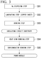
- a production method of a copper/ceramic bonded body of the present invention is a production method of a copper/ceramic bonded body for producing the above-described copper/ceramic bonded body, the production method including: a Mg-disposing step of disposing Mg between the copper member and the ceramic member; a laminating step of laminating the copper member and the ceramic member with Mg interposed therebetween; and a bonding step of performing a heating treatment on the copper member and the ceramic member laminated with Mg interposed therebetween in a state of being pressed in a laminating direction under a vacuum atmosphere to bond the copper member and the ceramic member to each other, in which, in the Mg-disposing step, an amount of Mg is in a range of 0.17 mg/cm 2 or more and 3.48 mg/cm 2 or less.
- the amount of Mg is in a range of 0.17 mg/cm 2 or more and 3.48 mg/cm 2 or less, a liquid phase necessary for the interfacial reaction can be sufficiently obtained. Therefore, it becomes possible to obtain the copper/ceramic bonded body in which the copper member and the ceramic member are reliably bonded to each other.
- Ti, Zr, Nb, and Hf are not used for bonding, a nitride phase of Ti, Zr, Nb, and Hf and an intermetallic compound phase containing Ti, Zr, Nb, and Hf are not present in the vicinity of the bonding surface of the ceramic member, and the copper/ceramic bonded body capable of suppressing breaking of the ceramic member during high-temperature operation can be obtained.
- a pressing load be in a range of 0.049 MPa or more and 3.4 MPa or less, and a heating temperature be in a range of 500°C or higher and 850°C or lower.
- the pressing load in the bonding step is in a range of 0.049 MPa or more and 3.4 MPa or less, the ceramic member, the copper member, and Mg can be brought into close contact, so that the interfacial reactions therebetween during heating can be promoted.
- the heating temperature in the bonding step is equal to or higher than 500°C, which is higher than the eutectic temperature of Cu and Mg, a liquid phase can be sufficiently generated at the bonded interface.
- the heating temperature in the bonding step is 850°C or lower, the excessive generation of the liquid phase can be suppressed. Furthermore, the thermal load on the ceramic member is reduced, so that the deterioration of the ceramic member can be suppressed.
- a production method of an insulating circuit substrate of the present invention is a production method of an insulating circuit substrate for producing the above-described insulating circuit substrate, the production method including: a Mg-disposing step of disposing Mg between the copper sheet and the ceramic substrate; a laminating step of laminating the copper sheet and the ceramic substrate with Mg interposed therebetween; and a bonding step of performing a heating treatment on the copper sheet and the ceramic substrate laminated with Mg interposed therebetween in a state of being pressed in a laminating direction under a vacuum atmosphere to bond the copper sheet and the ceramic substrate to each other, in which, in the Mg-disposing step, an amount of Mg is in a range of 0.17 mg/cm 2 or more and 3.48 mg/cm 2 or less.
- the amount of Mg is in a range of 0.17 mg/cm 2 or more and 3.48 mg/cm 2 or less, a liquid phase necessary for the interfacial reaction can be sufficiently obtained. Therefore, it becomes possible to obtain the insulating circuit substrate in which the copper sheet and the ceramic substrate are reliably bonded to each other.
- a nitride phase of Ti, Zr, Nb, and Hf and an intermetallic compound phase containing Ti, Zr, Nb, and Hf are not present in the vicinity of the bonding surface of the ceramic substrate, and the insulating circuit substrate capable of suppressing breaking of the ceramic substrate during high-temperature operation can be obtained.
- the insulating circuit substrate excellent in migration resistance can be obtained.
- a pressing load be in a range of 0.049 MPa or more and 3.4 MPa or less, and a heating temperature be in a range of 500°C or higher and 850°C or lower.
- the pressing load in the bonding step is in a range of 0.049 MPa or more and 3.4 MPa or less, the ceramic substrate, the copper sheet, and Mg can be brought into close contact, so that the interfacial reactions therebetween during heating can be promoted.
- the heating temperature in the bonding step is equal to or higher than 500°C, which is higher than the eutectic temperature of Cu and Mg, a liquid phase can be sufficiently generated at the bonded interface.
- the heating temperature in the bonding step is 850°C or lower, the excessive generation of the liquid phase can be suppressed. Furthermore, the thermal load on the ceramic substrate is reduced, so that the deterioration of the ceramic substrate can be suppressed.
- the present invention it becomes possible to provide a copper/ceramic bonded body in which a copper member and a ceramic member are reliably bonded to each other, excellent migration resistance is achieved, and the occurrence of ceramic breaking during high-temperature operation can be suppressed, an insulating circuit substrate, a production method of the copper/ceramic bonded body, and a production method of the insulating circuit substrate.
- a copper/ceramic bonded body according to the present embodiment is an insulating circuit substrate 10 configured by bonding a ceramic substrate 11 which is a ceramic member to a copper sheet 22 (circuit layer 12) and to a copper sheet 23 (metal layer 13), which are copper members.
- Fig. 1 illustrates the insulating circuit substrate 10 according to the embodiment of the present invention and a power module 1 using the insulating circuit substrate 10.
- the power module 1 includes the insulating circuit substrate 10, a semiconductor element 3 bonded to one side (upper side in Fig. 1 ) of the insulating circuit substrate 10 with a first solder layer 2 interposed therebetween, and a heat sink 51 bonded to the other side (lower side in Fig. 1 ) of the insulating circuit substrate 10 with a second solder layer 8 interposed therebetween.
- the insulating circuit substrate 10 includes the ceramic substrate 11, the circuit layer 12 disposed on one surface (upper surface in Fig. 1 ) of the ceramic substrate 11, and the metal layer 13 disposed on the other surface (lower surface in Fig. 1 ) of the ceramic substrate 11.
- the ceramic substrate 11 prevents the electrical connection between the circuit layer 12 and the metal layer 13, and is made of alumina, which is a kind of aluminum oxide, in the present embodiment.
- the thickness of the ceramic substrate 11 is set to be in a range of 0.2 mm or more and 1.5 mm or less, and in the present embodiment, the thickness of the ceramic substrate 11 is preferably 0.635 mm.
- the circuit layer 12 is formed by bonding the copper sheet 22 made of copper or a copper alloy to one surface of the ceramic substrate 11.
- a rolled sheet of oxygen-free copper is used as the copper sheet 22 constituting the circuit layer 12.
- a circuit pattern is formed on the circuit layer 12, and one surface thereof (upper surface in Fig. 1 ) becomes a mounting surface on which the semiconductor element 3 is mounted.
- the thickness of the circuit layer 12 is set to be in a range of 0.1 mm or more and 1.0 mm or less, and in the present embodiment, the thickness of the circuit layer 12 is preferably 0.6 mm.
- the metal layer 13 is formed by bonding the copper sheet 23 made of copper or a copper alloy to the other surface of the ceramic substrate 11.
- a rolled sheet of oxygen-free copper is used as the copper sheet 23 constituting the metal layer 13.
- the thickness of the metal layer 13 is set to be in a range of 0.1 mm or more and 1.0 mm or less, and in the present embodiment, the thickness of the metal layer 13 is preferably 0.6 mm.
- the heat sink 51 is for cooling the above-mentioned insulating circuit substrate 10, and in the present embodiment, is a heat-dissipating sheet made of a material having good thermal conductivity.
- the heat sink 51 is made of copper or a copper alloy excellent in thermal conductivity.
- the heat sink 51 and the metal layer 13 of the insulating circuit substrate 10 are bonded to each other with the second solder layer 8 interposed therebetween.
- the ceramic substrate 11 and the circuit layer 12 (copper sheet 22), and the ceramic substrate 11 and the metal layer 13 (copper sheet 23) are bonded to each other with a Mg film 25 interposed therebetween as illustrated in Fig. 4 .
- a structure in which a magnesium oxide layer 31 formed on the ceramic substrate 11 side of the bonded interface and a Mg solid solution layer 32 in which Mg is in a state of a solid solution in a Cu primary phase are laminated is provided.
- the magnesium oxide layer 31 is made of, for example, MgO.
- the thickness of the magnesium oxide layer 31 is in a range of 0.05 ⁇ m or more and 1.0 ⁇ m or less, and preferably in a range of 0.1 ⁇ m or more and 0.5 ⁇ m or less. It is presumed that the magnesium oxide layer 31 is formed by the reaction of oxygen (O) of the oxide formed on the surface of the ceramic substrate 11 and magnesium (Mg) of the Mg film 25.
- the amount of Mg in the Mg solid solution layer 32 is in a range of 0.01 at% or more and 3 at% or less.
- the thickness of the Mg solid solution layer 32 is in a range of 0.1 ⁇ m or more and 150 ⁇ m or less, and preferably in a range of 0.1 ⁇ m or more and 80 ⁇ m or less.
- the area ratio of an intermetallic compound phase in a region from the bonding surface of the ceramic substrate 11 to 50 ⁇ m toward the copper sheet 22 (circuit layer 12) and the copper sheet 23 (metal layer 13) side be 15% or less.
- a Cu-Mg intermetallic compound phase containing Cu and Mg may be dispersed inside the Mg solid solution layer 32.
- Examples of the Cu-Mg intermetallic compound phase include Cu 2 Mg and CuMg2.
- Mg is disposed between the copper sheet 22 which is to become the circuit layer 12 and the ceramic substrate 11 and between the copper sheet 23 which is to become the metal layer 13 and the ceramic substrate 11.
- the Mg film 25 is formed by vapor deposition of Mg.
- the amount of Mg to be disposed is in a range of 0.17 mg/cm 2 or more and 3.48 mg/cm 2 or less.
- the copper sheet 22 and the ceramic substrate 11 are laminated with the Mg film 25 interposed therebetween, and the ceramic substrate 11 and the copper sheet 23 are laminated with the Mg film 25 interposed therebetween.
- the copper sheet 22, the ceramic substrate 11, and the copper sheet 23 which are laminated are pressed in a laminating direction and are loaded into a vacuum furnace and heated such that the copper sheet 22, the ceramic substrate 11, and the copper sheet 23 are bonded together.
- the pressing load in the bonding step S03 is preferably in a range of 0.049 MPa or more and 3.4 MPa or less.
- the heating temperature in the bonding step S03 is preferably in a range of 500°C or higher and 850°C or lower.
- the degree of vacuum in the bonding step S03 is preferably in a range of 1 ⁇ 10 -6 Pa or more and 5 ⁇ 10 -2 Pa or less.
- the retention time at the heating temperature is preferably in a range of 5 minutes or longer and 180 minutes or shorter.
- the temperature-lowering rate when the temperature is lowered from the heating temperature (bonding temperature) to 480°C is not particularly limited, but is preferably 20°C/min or less, and more preferably 15°C/min or less.
- the lower limit of the temperature-lowering rate is not particularly limited, but may be 2.5°C/min or more, or 5°C/min or more.
- the insulating circuit substrate 10 according to the present embodiment is produced by the Mg-disposing step S01, the laminating step S02, and the bonding step S03.
- the heat sink 51 is bonded to the other surface side of the metal layer 13 of the insulating circuit substrate 10.
- the insulating circuit substrate 10 and the heat sink 51 are laminated with the solder material interposed therebetween and are loaded into a heating furnace such that the insulating circuit substrate 10 and the heat sink 51 are soldered to each other with the second solder layer 8 interposed therebetween.
- the semiconductor element 3 is bonded to one surface of the circuit layer 12 of the insulating circuit substrate 10 by soldering.
- the power module 1 illustrated in Fig. 1 is produced by the above steps.
- the copper sheet 22 (circuit layer 12) and the copper sheet 23 (metal layer 13) made of oxygen-free copper and the ceramic substrate 11 made of an aluminum oxide (alumina) are bonded to each other with the Mg film 25 interposed therebetween, and the magnesium oxide layer 31 is formed on the ceramic substrate 11 side between the ceramic substrate 11 and the circuit layer 12 (copper sheet 22) and between the ceramic substrate 11 and the metal layer 13 (copper sheet 23).
- the magnesium oxide layer 31 is formed by the reaction between Mg interposed between the copper sheet 22 (circuit layer 12) and the copper sheet 23 (metal layer 13) and the ceramic substrate 11 and oxygen in the ceramic substrate 11, and thus the ceramic substrate 11 sufficiently reacts.
- an interfacial reaction proceeds sufficiently at the bonded interfaces between the copper sheet 22 (circuit layer 12) and the copper sheet 23 (metal layer 13) and the ceramic substrate 11, so that the insulating circuit substrate 10 (copper/ceramic bonded body) in which the copper sheet 22 (circuit layer 12) and the copper sheet 23 (metal layer 13) and the ceramic substrate 11 are reliably bonded can be obtained.
- Ti, Zr, Nb, and Hf are not present at the bonded interfaces between the copper sheet 22 (circuit layer 12) and the copper sheet 23 (metal layer 13) and the ceramic substrate 11, a nitride phase of Ti, Zr, Nb, and Hf and an intermetallic compound phase containing Ti, Zr, Nb, and Hf are not generated, and breaking of the ceramic substrate 11 can be suppressed even during high-temperature operation.
- the total amount of Ti, Zr, Nb, and Hf at the bonded interfaces between the copper sheet 22 (circuit layer 12) and the copper sheet 23 (metal layer 13) and the ceramic substrate 11 is preferably 0.3 mass% or less, and preferably 0.1 mass% or less.
- the amount of Ag at the bonded interfaces between the copper sheet 22 (circuit layer 12) and the copper sheet 23 (metal layer 13) and the ceramic substrate 11 is preferably 0.2 mass% or less, and more preferably 0.1 mass% or less.
- the area ratio of the intermetallic compound phase in the region from the bonding surface of the ceramic substrate 11 to 50 ⁇ m toward the copper sheet 22 (circuit layer 12) and the copper sheet 23 (metal layer 13) side is 15% or less, there are not a large number of hard and brittle intermetallic compound phases in the vicinity of the bonding surface of the ceramic substrate 11, and it becomes possible to reliably suppress breaking of the ceramic substrate 11 during high-temperature operation.
- the area ratio of the intermetallic compound phase in the region from the bonding surface of the ceramic substrate 11 to 50 ⁇ m toward the copper sheet 22 (circuit layer 12) and the copper sheet 23 (metal layer 13) side is preferably 10% or less, and more preferably 8% or less.
- the laminating step S02 of laminating the copper sheets 22 and 23 and the ceramic substrate 11 with the Mg film 25 interposed therebetween, and the bonding step S03 of performing the heating treatment on the copper sheet 22, the ceramic substrate 11, and the copper sheet 23 which are laminated in a state of being pressed in the laminating direction under a vacuum atmosphere to bond the copper sheet 22, the ceramic substrate 11, and the copper sheet 23 together are provided, no gas or no residue of organic matter remains at the bonded interface.
- the insulating circuit substrate 10 (copper/ceramic bonded body) in which the copper sheets 22 and 23 and the ceramic substrate 11 are reliably bonded can be obtained.
- a nitride phase of Ti, Zr, Nb, and Hf and an intermetallic compound phase containing Ti, Zr, Nb, and Hf are not present in the vicinity of the bonding surface of the ceramic substrate 11, and the insulating circuit substrate 10 (copper/ceramic bonded body) capable of suppressing breaking of the ceramic substrate 11 during high-temperature operation can be obtained.
- the insulating circuit substrate 10 (copper/ceramic bonded body) excellent in migration resistance can be obtained.
- the amount of Mg is less than 0.17 mg/cm 2 , the amount of the generated liquid phase is insufficient, and there is concern that the bonding rate may decrease. In a case where the amount of Mg exceeds 3.48 mg/cm 2 , the amount of the generated liquid phase becomes excessive, the liquid phase may leak from the bonded interface, and there is concern that a bonded body having a predetermined shape may not be produced. Furthermore, the Cu-Mg intermetallic compound phase may be excessively generated, and there is concern that breaking may occur in the ceramic substrate 11.
- the amount of Mg is in a range of 0.17 mg/cm 2 or more and 3.48 mg/cm 2 or less.
- the lower limit of the amount of Mg is preferably 0.24 mg/cm 2 or more, and more preferably 0.32 mg/cm 2 or more.
- the upper limit of the amount of Mg is preferably 2.38 mg/cm 2 or less, and more preferably 1.58 mg/cm 2 or less.
- the pressing load in the bonding step S03 is 0.049 MPa or more, the ceramic substrate 11, the copper sheets 22 and 23, and the Mg film 25 can be brought into close contact, so that the interfacial reactions therebetween during heating can be promoted. Since the pressing load in the bonding step S03 is 3.4 MPa or less, breaking and the like in the ceramic substrate 11 in the bonding step S03 can be suppressed.
- the lower limit of the pressing load in the bonding step S03 is preferably 0.098 MPa or more, and more preferably 0.294 MPa or more.
- the upper limit of the pressing load in the bonding step S03 is preferably 1.96 MPa or less, and more preferably 0.98 MPa or less.
- the heating temperature in the bonding step S03 is equal to or higher than 500°C, which is higher than the eutectic temperature of Cu and Mg, a liquid phase can be sufficiently generated at the bonded interface.
- the heating temperature in the bonding step S03 is 850°C or lower, the excessive generation of the liquid phase can be suppressed. Furthermore, the thermal load on the ceramic substrate 11 is reduced, so that the deterioration of the ceramic substrate 11 can be suppressed.
- the lower limit of the heating temperature in the bonding step S03 is preferably 600°C or higher, and more preferably 680°C or higher.
- the upper limit of the heating temperature in the bonding step S03 is preferably 800°C or lower, and more preferably 760°C or lower.
- the degree of vacuum in the bonding step S03 is in a range of 1 ⁇ 10 -6 Pa or more and 5 ⁇ 10 -2 Pa or less, the oxidation of the Mg film 25 can be suppressed, and it becomes possible to reliably bond the ceramic substrate 11 and the copper sheets 22 and 23.
- the lower limit of the degree of vacuum in the bonding step S03 is preferably 1 ⁇ 10 -4 Pa or more, and more preferably 1 ⁇ 10 -3 Pa or more.
- the upper limit of the degree of vacuum in the bonding step S03 is preferably 1 ⁇ 10 -2 Pa or less, and more preferably 5 ⁇ 10 -3 Pa or less.
- the retention time at the heating temperature in the bonding step S03 is in a range of 5 minutes or longer and 180 minutes or shorter, a liquid phase can be sufficiently formed, and it becomes possible to reliably bond the ceramic substrate 11 and the copper sheets 22 and 23.
- the lower limit of the retention time at the heating temperature in the bonding step S03 is preferably 10 minutes or longer, and more preferably 30 minutes or longer.
- the upper limit of the retention time at the heating temperature in the bonding step S03 is preferably 150 minutes or shorter, and more preferably 120 minutes or shorter.
- the copper sheet which constitutes the circuit layer or the metal layer is described as the rolled sheet of oxygen-free copper, the copper sheet is not limited thereto, and may also be made of another kind of copper or copper alloy.
- circuit layer and the metal layer are described as being constituted by the copper sheets, the circuit layer and the metal layer are not limited thereto. As long as at least one of the circuit layer and the metal layer is constituted by a copper sheet, the other may be constituted by another metal sheet such as an aluminum sheet.
- the Mg film is not limited thereto, and the Mg film may be formed by another method, or a Mg foil may be disposed. Alternatively, a clad material of Cu and Mg may be disposed.
- a Mg paste and a Cu-Mg paste may be applied.
- a Cu paste and a Mg paste may be laminated and disposed.
- the Mg paste may be disposed on either the copper sheet side or the ceramic substrate side.
- MgH 2 may be disposed as Mg.
- the heat sink is exemplified by the heat-dissipating sheet, the heat sink is not limited thereto, and there is no particular limitation on the structure of the heat sink. For example, one having a passage through which a refrigerant flows or one having a cooling fin may be used.
- a composite material for example, AlSiC
- aluminum or an aluminum alloy can also be used.
- a buffer layer made of aluminum or an aluminum alloy or a composite material (for example, AlSiC) containing aluminum may be provided between the top sheet part or heat-dissipating sheet of the heat sink and the metal layer.
- an LED module may be configured by mounting an LED element on the insulating circuit substrate, or a thermoelectric module may be configured by mounting a thermoelectric element on the circuit layer of the insulating circuit substrate.
- a copper/ceramic bonded body was formed by laminating copper sheets (oxygen-free copper, 37 mm square, thickness 0.15 mm) in which Mg was disposed as shown in Table 1, on both surfaces of a 40 mm square ceramic substrate made of an aluminum oxide (alumina) and bonding the laminated sheets under bonding conditions shown in Table 1.
- the thickness of the ceramic substrate was 0.635 mm.
- the degree of vacuum of the vacuum furnace at the time of bonding was 5 ⁇ 10 -3 Pa.
- an active brazing material of Ag-28 mass% Cu-5 mass% Ti was disposed between the ceramic substrate and the copper sheet so that the amount of Ag was 5.2 mg/cm 2 .
- the temperature-lowering rate was controlled to be a rate of 5°C/min.
- the temperature-lowering rate is controlled by the partial pressure of a gas during gas cooling (whether or not circulation is performed by a cooling fan).
- the bonded interface was observed, and a magnesium oxide layer, a Mg solid solution layer, and a Cu-Mg intermetallic compound phase were checked.
- the initial bonding rate of the copper/ceramic bonded body, breaking of the ceramic substrate after thermal cycles, and migration properties were evaluated as follows.
- the bonded interface between the copper sheet and the ceramic substrate was observed using a transmission electron microscope (Titan ChemiSTEM manufactured by FEI Company) at an accelerating voltage of 200 kV and a magnification of 40,000 times, and in the element mapping obtained, a case where a region where Mg and O coexisted was present was evaluated as a magnesium oxide layer "present".
- a region (400 ⁇ m ⁇ 600 ⁇ m) including the bonded interface was observed under the conditions of a magnification of 2,000 times and an accelerating voltage of 15 kV using an EPMA apparatus (JXA-8539F manufactured by JEOL Ltd.), quantitative analysis was performed on a range of 10 points or more and 20 points or less depending on the thickness of the copper sheet at intervals of 10 ⁇ m from the surface of the ceramic substrate toward the copper sheet side, and a region having a Mg concentration of 0.01 at% or more was regarded as a Mg solid solution layer.
- an element map of Mg of the region (400 ⁇ m ⁇ 600 ⁇ m) including the bonded interface was acquired under the conditions of a magnification of 2,000 times and an accelerating voltage of 15 kV using an electron micro analyzer (JXA-8539F manufactured by JEOL Ltd.), and a region satisfying that the Cu concentration as a five-point average of quantitative analysis in the region where the presence of Mg was confirmed was 5 at% or more and the Mg concentration was 30 at% or more and 70 at% or less was regarded as a Cu-Mg intermetallic compound phase.
- the area ratio (%) of the intermetallic compound phase in the region from the bonding surface of the ceramic substrate to 50 ⁇ m toward the copper sheet side was calculated.
- the bonding rate between the copper sheet and the ceramic substrate was obtained using the following equation using an ultrasonic flaw detector (FineSAT200 manufactured by Hitachi Power Solutions Co., Ltd.).
- the initial bonding area was the area to be bonded before bonding, that is, the area of the bonding surface of the copper sheet.
- peeling was indicated by a white portion in the bonding part, and thus the area of the white portion was regarded as a peeled area.
- Initial bonding rate initial bonding area ⁇ peeled area / ( initial bonding area )
- TSA-72ES thermal shock tester
- the electric resistance between circuit patterns was measured after being left for 2,000 hours under the conditions of a distance between the circuit patterns separated by insulation in a circuit layer of 0.5 mm, a temperature of 85°C, a humidity of 85%RH, and a voltage of DC50V.
- a case where the resistance value was 1 ⁇ 10 6 ⁇ or less was determined as a short-circuit (migration had occurred), and the migration was evaluated as "B".
- the electric resistance between the circuit patterns was measured.
- a case where the resistance value was greater than 1 ⁇ 10 6 ⁇ was determined as the absence of migration, and the migration was evaluated as "A".
- Example 3 The evaluation results are shown in Table 2. In addition, the observation results of Example 3 are shown in Fig. 5 .
- [Table 1] Mg-disposing step Bonding step Amount of Mg mg/cm 2 Load MPa Temperature °C Time min Example 1 0.21 0.098 650 150 Example 2 1.11 3.4 720 120 Example 3 0.17 0.049 780 120 Example 4 3.01 0.294 500 30 Example 5 0.32 0.098 720 180 Example 6 0.24 0.294 600 10 Example 7 2.06 3.4 680 30 Example 8 2.38 0.98 810 90 Example 9 0.27 3.4 720 5 Example 10 3.48 3.4 800 60 Example 11 1.58 0.098 760 90 Example 12 0.79 0.294 760 90 Comparative Example 1 0.11 3.4 810 90 Comparative Example 2 5.54 0.049 760 90 Related Art Example (Active brazing material) 0.98 810 90 [Table 2] Observation result of bonded interface Initial bonding rate % Presence or absence of ceramic breaking Migration Magnesium Oxide Layer Mg solid solution
- Copper/ceramic bonded bodies according to Examples 21 to 32 were produced in the same manner as the copper/ceramic bonded bodies produced in Examples 1 to 12, and regarding the obtained copper/ceramic bonded bodies, the area ratio of Cu 2 Mg and an ultrasonic bonded interface were evaluated as follows.
- the area ratio (%) of Cu 2 Mg was defined and calculated by the following calculation formula.
- Area ratio % of Cu 2 Mg area of Cu 2 Mg / area of Cu 2 Mg + area of CuMg 2 ⁇ 100
- Rea of Cu 2 Mg was a region in which the Mg concentration was 30 at% or more and less than 60 at%, and "area of CuMg2" was a region in which the Mg concentration was 60 at% or more and less than 70 at%.
- Example 21 1.11 3.4 720 120 5 Present Present Present 6.3 93.7 97.5 A
- Example 22 1.11 3.4 720 120 7 Present Present 6.9 92.4 98.3 A
- Example 23 1.11 3.4 720 120 12 Present Present Present 6.5 85.3 98.1 A
- Example 24 1.11 3.4 720 120 24 Present Present 6.5 62.9 98.3 B
- Example 25 2.38 0.98 810 90 5 Present Present Present 6.9 92.7 99.2 A
- Example 26 2.38 0.98 810 90 10 Present Present Present Present Present 6.1 90.0 99.4 A
- Example 27 2.38 0.98 810 90 20 Present Present Present Present 6.6 70.3 97.8 A
- Example 28 2.38 0.98 810 90 35 Present Present Present 6.7 51.4 98.2 C
- Example 29 3.48 3.4 800 60 2.5 Present Present Present 10.0 97.5 98.6 A
- Example 30 3.48 3.4 800 60 5 Present Present Present 9.8 98.5 97.5 A
- Example 31 3.48 3.4 800 60 15 Present Present Present 9.3 79.8 98.
- the value of the area ratio of Cu 2 Mg and the bonding properties of ultrasonic bonding changed depending on the temperature-lowering rate after the bonding step S03.
- the temperature-lowering rate is preferably 20°C/min or less, and more preferably 15°C/min or less.
- the area ratio of Cu 2 Mg is preferably 70% or more, more preferably 80% or more, and even more preferably 90% or more.
- Copper/ceramic bonded bodies according to Examples 41 to 52 were produced in the same manner as the copper/ceramic bonded bodies produced in Examples 1 to 12, and regarding the obtained copper/ceramic bonded bodies, the thickness of the magnesium oxide layer and the number of cycles at which ceramic breaking had occurred were evaluated as follows.
- the bonded interface between the copper sheet and the ceramic substrate was observed using a transmission electron microscope (Titan ChemiSTEM manufactured by FEI Company) at an accelerating voltage of 200 kV and a magnification of 20,000 times, and in the element mapping obtained, a case where a region where Mg and O coexisted was identified as a magnesium oxide layer.
- the magnesium oxide layer may contain any of magnesia (MgO) and spinel (MgAl 2 O 4 ).
- the thickness of the magnesium oxide layer was calculated by dividing the area of the magnesium oxide layer by the observation width in the observation visual field.
- thermal shock tester (TSA-72ES manufactured by ESPEC Corp.) a thermal cycle test was conducted by performing 300 cycles, where one cycle is 10 minutes at -50°C and 10 minutes at 175°C, in a gas phase.
- the presence or absence of breaking in the ceramic substrate was checked every 10 cycles.
- the presence or absence of ceramic breaking was determined from an interface inspection using the ultrasonic flaw detector (FineSAT200 manufactured by Hitachi Power Solutions Co., Ltd.).
- FineSAT200 manufactured by Hitachi Power Solutions Co., Ltd.
- Table 4 "> 300" indicates that no breaking was confirmed after 300 cycles.
- the magnesium oxide layer is preferably in a range of 0.05 ⁇ m or more and 2.00 ⁇ m or less, more preferably in a range of 0.05 ⁇ m or more and 0.80 ⁇ m or less, and even more preferably 0.05 ⁇ m or more and 0.07 ⁇ m or less.
- the present invention it becomes possible to provide a copper/ceramic bonded body in which a copper member and a ceramic member are reliably bonded to each other, excellent migration resistance is achieved, and the occurrence of ceramic breaking during high-temperature operation can be suppressed, an insulating circuit substrate, a production method of the copper/ceramic bonded body, and a production method of the insulating circuit substrate.
Landscapes
- Engineering & Computer Science (AREA)
- Chemical & Material Sciences (AREA)
- Ceramic Engineering (AREA)
- Materials Engineering (AREA)
- Structural Engineering (AREA)
- Organic Chemistry (AREA)
- Manufacturing & Machinery (AREA)
- Mechanical Engineering (AREA)
- Microelectronics & Electronic Packaging (AREA)
- Inorganic Chemistry (AREA)
- Ceramic Products (AREA)
- Cooling Or The Like Of Semiconductors Or Solid State Devices (AREA)
- Manufacturing Of Printed Wiring (AREA)
- Pressure Welding/Diffusion-Bonding (AREA)
- Structure Of Printed Boards (AREA)
- Laminated Bodies (AREA)
Applications Claiming Priority (2)
| Application Number | Priority Date | Filing Date | Title |
|---|---|---|---|
| JP2018159663 | 2018-08-28 | ||
| PCT/JP2019/033427 WO2020045386A1 (fr) | 2018-08-28 | 2019-08-27 | Corps assemblé en cuivre/céramique, carte de circuit imprimé isolée, et procédé de production de corps assemblé en cuivre/céramique, et procédé de fabrication de carte de circuit imprimé isolée |
Publications (2)
| Publication Number | Publication Date |
|---|---|
| EP3845510A1 true EP3845510A1 (fr) | 2021-07-07 |
| EP3845510A4 EP3845510A4 (fr) | 2022-06-08 |
Family
ID=69643027
Family Applications (1)
| Application Number | Title | Priority Date | Filing Date |
|---|---|---|---|
| EP19854223.5A Withdrawn EP3845510A4 (fr) | 2018-08-28 | 2019-08-27 | Corps assemblé en cuivre/céramique, carte de circuit imprimé isolée, et procédé de production de corps assemblé en cuivre/céramique, et procédé de fabrication de carte de circuit imprimé isolée |
Country Status (7)
| Country | Link |
|---|---|
| US (1) | US12037294B2 (fr) |
| EP (1) | EP3845510A4 (fr) |
| JP (1) | JP7136212B2 (fr) |
| KR (1) | KR20210044791A (fr) |
| CN (1) | CN112638843B (fr) |
| TW (2) | TW202144311A (fr) |
| WO (2) | WO2020044590A1 (fr) |
Families Citing this family (10)
| Publication number | Priority date | Publication date | Assignee | Title |
|---|---|---|---|---|
| JP7119268B2 (ja) * | 2020-05-27 | 2022-08-17 | 三菱マテリアル株式会社 | 銅/セラミックス接合体、および、絶縁回路基板 |
| US11866372B2 (en) | 2020-05-28 | 2024-01-09 | Saudi Arabian Oil Company | Bn) drilling tools made of wurtzite boron nitride (W-BN) |
| CN116783019A (zh) * | 2020-06-02 | 2023-09-19 | 沙特阿拉伯石油公司 | 生产无催化剂pdc刀具 |
| IT202000016840A1 (it) * | 2020-07-10 | 2022-01-10 | St Microelectronics Srl | Dispositivo mosfet incapsulato ad alta tensione e dotato di clip di connessione e relativo procedimento di fabbricazione |
| US12024470B2 (en) | 2021-02-08 | 2024-07-02 | Saudi Arabian Oil Company | Fabrication of downhole drilling tools |
| WO2022230220A1 (fr) | 2021-04-28 | 2022-11-03 | 富士電機株式会社 | Dispositif à semi-conducteurs |
| JP7694291B2 (ja) * | 2021-09-21 | 2025-06-18 | 三菱マテリアル株式会社 | 銅/セラミックス接合体、および、絶縁回路基板 |
| JP7647471B2 (ja) * | 2021-09-21 | 2025-03-18 | 三菱マテリアル株式会社 | 銅/セラミックス接合体、および、絶縁回路基板 |
| TWI841253B (zh) * | 2023-02-22 | 2024-05-01 | 碁曄科技股份有限公司 | 活性金屬焊接陶瓷基板之製備方法 |
| KR102908800B1 (ko) * | 2023-07-24 | 2026-01-07 | (주)코스텍시스 | 회로기판의 제조방법 및 회로기판 |
Family Cites Families (39)
| Publication number | Priority date | Publication date | Assignee | Title |
|---|---|---|---|---|
| JPS60131875A (ja) | 1983-12-20 | 1985-07-13 | 三菱重工業株式会社 | セラミツクと金属の接合法 |
| US4639388A (en) * | 1985-02-12 | 1987-01-27 | Chromalloy American Corporation | Ceramic-metal composites |
| JPS63220987A (ja) | 1987-03-06 | 1988-09-14 | Natl Res Inst For Metals | アルミニウム及びアルミナセラミツクスの拡散接合法 |
| JPH02307875A (ja) * | 1989-05-18 | 1990-12-21 | Aisin Seiki Co Ltd | セラミツクスと金属の接合方法 |
| JPH03112874A (ja) * | 1989-09-26 | 1991-05-14 | Matsushita Electric Works Ltd | セラミック基体と銅の接合方法 |
| JPH04162756A (ja) | 1990-10-26 | 1992-06-08 | Toshiba Corp | 半導体モジュール |
| JP3211856B2 (ja) | 1994-11-02 | 2001-09-25 | 電気化学工業株式会社 | 回路基板 |
| JP3866320B2 (ja) | 1995-02-09 | 2007-01-10 | 日本碍子株式会社 | 接合体、および接合体の製造方法 |
| JPH09153567A (ja) * | 1995-09-28 | 1997-06-10 | Toshiba Corp | 高熱伝導性窒化珪素回路基板および半導体装置 |
| FR2751640B1 (fr) | 1996-07-23 | 1998-08-28 | Commissariat Energie Atomique | Composition et procede de brasage reactif de materiaux ceramiques contenant de l'alumine |
| DE19953670A1 (de) | 1999-11-08 | 2001-05-23 | Euromat Gmbh | Lotlegierung |
| US6989200B2 (en) | 2003-10-30 | 2006-01-24 | Alfred E. Mann Foundation For Scientific Research | Ceramic to noble metal braze and method of manufacture |
| JP4375730B2 (ja) | 2004-04-23 | 2009-12-02 | 本田技研工業株式会社 | 銅とセラミックス又は炭素基銅複合材料との接合用ろう材及び同接合方法 |
| CN101391901B (zh) | 2008-11-07 | 2010-08-11 | 哈尔滨工业大学 | Al2O3陶瓷与金属材料的钎焊方法 |
| JP5359936B2 (ja) | 2010-03-03 | 2013-12-04 | 三菱マテリアル株式会社 | パワーモジュール用基板、パワーモジュール用基板の製造方法、ヒートシンク付パワーモジュール用基板及びパワーモジュール |
| JP5577980B2 (ja) | 2010-09-16 | 2014-08-27 | 三菱マテリアル株式会社 | ヒートシンク付パワーモジュール用基板、パワーモジュール及びヒートシンク付パワーモジュール用基板の製造方法 |
| KR101548091B1 (ko) * | 2011-07-28 | 2015-08-27 | 가부시끼가이샤 도시바 | 산화물계 세라믹스 회로 기판의 제조 방법 및 산화물계 세라믹스 회로 기판 |
| JP2013071873A (ja) | 2011-09-28 | 2013-04-22 | Nhk Spring Co Ltd | 接合体 |
| CN102489805B (zh) | 2011-11-11 | 2014-06-04 | 西安交通大学 | 在铝基复合材料钎缝中能获得原位强化相的钎料设计方法及适于铸铝基体的Al-Cu-Ti系活性钎料 |
| CN102554385B (zh) | 2011-12-13 | 2013-09-04 | 河南科技大学 | 一种金属陶瓷复合衬板的钎焊铸接工艺 |
| JP5910166B2 (ja) * | 2012-02-29 | 2016-04-27 | 三菱マテリアル株式会社 | パワーモジュール用基板の製造方法 |
| JP6111764B2 (ja) | 2013-03-18 | 2017-04-12 | 三菱マテリアル株式会社 | パワーモジュール用基板の製造方法 |
| JP6038698B2 (ja) | 2013-03-22 | 2016-12-07 | 日本碍子株式会社 | セラミックス部材及び半導体製造装置用部材 |
| CN103231181A (zh) | 2013-03-28 | 2013-08-07 | 杭州碳诺光伏材料有限公司 | 低成本、环保型氧化物陶瓷靶材与铜背板焊接的研究 |
| KR101758586B1 (ko) | 2014-02-12 | 2017-07-14 | 미쓰비시 마테리알 가부시키가이샤 | 구리/세라믹스 접합체 및 파워 모듈용 기판 |
| US9735085B2 (en) * | 2014-03-20 | 2017-08-15 | Mitsubishi Materials Corporation | Bonded body, power module substrate, power module and method for producing bonded body |
| JP2015224151A (ja) * | 2014-05-27 | 2015-12-14 | Ngkエレクトロデバイス株式会社 | Cu/セラミック基板 |
| WO2016039060A1 (fr) * | 2014-09-10 | 2016-03-17 | コニカミノルタ株式会社 | Film barrière aux gaz et élément électroluminescent organique |
| CN106687864B (zh) * | 2014-11-26 | 2020-07-03 | 日立化成株式会社 | 感光性树脂组合物、感光性元件、固化物、半导体装置、抗蚀图案的形成方法及电路基材的制造方法 |
| JP6656657B2 (ja) * | 2015-11-06 | 2020-03-04 | 三菱マテリアル株式会社 | セラミックス/アルミニウム接合体、パワーモジュール用基板、及び、パワーモジュール |
| CN105458547B (zh) | 2015-12-28 | 2017-12-15 | 西安交通大学 | 一种适于高体积分数SiC强化的铸铝基复合材料的活性钎料及其制备方法 |
| JP6822247B2 (ja) | 2016-03-25 | 2021-01-27 | 三菱マテリアル株式会社 | ヒートシンク付絶縁回路基板の製造方法 |
| JP6904088B2 (ja) | 2016-06-30 | 2021-07-14 | 三菱マテリアル株式会社 | 銅/セラミックス接合体、及び、絶縁回路基板 |
| JP6658400B2 (ja) * | 2016-08-24 | 2020-03-04 | 三菱マテリアル株式会社 | セラミックス/Al−SiC複合材料接合体の製造方法、及びヒートシンク付パワーモジュール用基板の製造方法 |
| CN106825978B (zh) | 2017-02-24 | 2019-08-27 | 哈尔滨工业大学深圳研究生院 | 一种用于陶瓷与金属焊接的钎料及焊接方法 |
| JP6807060B2 (ja) | 2017-03-23 | 2021-01-06 | 桐生電子開発合同会社 | 血糖値変化量測定装置 |
| JP3211856U (ja) | 2017-05-09 | 2017-08-10 | 株式会社アイエスピー | メジャー付きタオル |
| CN113727838A (zh) * | 2019-04-26 | 2021-11-30 | 柯尼卡美能达株式会社 | 透明电极和具备该透明电极的电子设备 |
| EP4084029A4 (fr) * | 2019-12-25 | 2024-09-18 | Dai Nippon Printing Co., Ltd. | Matériau extérieur pour dispositif de stockage électrique, son procédé de fabrication et dispositif de stockage électrique |
-
2019
- 2019-02-04 WO PCT/JP2019/003834 patent/WO2020044590A1/fr not_active Ceased
- 2019-02-14 TW TW108104875A patent/TW202144311A/zh unknown
- 2019-08-26 TW TW108130463A patent/TWI796514B/zh not_active IP Right Cessation
- 2019-08-27 WO PCT/JP2019/033427 patent/WO2020045386A1/fr not_active Ceased
- 2019-08-27 EP EP19854223.5A patent/EP3845510A4/fr not_active Withdrawn
- 2019-08-27 KR KR1020217004790A patent/KR20210044791A/ko not_active Ceased
- 2019-08-27 US US17/270,133 patent/US12037294B2/en active Active
- 2019-08-27 JP JP2020539467A patent/JP7136212B2/ja active Active
- 2019-08-27 CN CN201980056167.0A patent/CN112638843B/zh active Active
Also Published As
| Publication number | Publication date |
|---|---|
| WO2020045386A1 (fr) | 2020-03-05 |
| TW202144311A (zh) | 2021-12-01 |
| US20210238102A1 (en) | 2021-08-05 |
| CN112638843B (zh) | 2022-11-11 |
| TWI796514B (zh) | 2023-03-21 |
| US12037294B2 (en) | 2024-07-16 |
| EP3845510A4 (fr) | 2022-06-08 |
| CN112638843A (zh) | 2021-04-09 |
| JPWO2020045386A1 (ja) | 2021-08-12 |
| KR20210044791A (ko) | 2021-04-23 |
| WO2020044590A1 (fr) | 2020-03-05 |
| TW202016051A (zh) | 2020-05-01 |
| JP7136212B2 (ja) | 2022-09-13 |
Similar Documents
| Publication | Publication Date | Title |
|---|---|---|
| EP3845510A1 (fr) | Corps assemblé en cuivre/céramique, carte de circuit imprimé isolée, et procédé de production de corps assemblé en cuivre/céramique, et procédé de fabrication de carte de circuit imprimé isolée | |
| EP3845509B1 (fr) | Corps assemblé en cuivre/céramique, carte de circuit imprimé isolée, procédé de production de corps assemblé en cuivre/céramique, et procédé de fabrication de carte de circuit imprimé isolée | |
| EP3590909B1 (fr) | Carte de circuit imprimé isolée à corps assemblé en cuivre/céramique, procédé de production de corps assemblé en cuivre/céramique, et procédé de production de carte de circuit imprimé isolée | |
| EP3744705B1 (fr) | Corps lié cuivre/céramique, carte de circuit imprimé isolante, procédé de production de corps lié cuivre/céramique, et procédé de production de carte de circuit imprimé isolante | |
| EP2980843B1 (fr) | Module d'alimentation | |
| EP4019483A1 (fr) | Ensemble cuivre/céramique, carte de circuit imprimé isolée, procédé de production d'ensemble cuivre/céramique et procédé de production de carte de circuit imprimé isolée | |
| EP3845511B1 (fr) | Corps assemblé en cuivre/céramique, carte de circuit imprimé isolée, procédé de production de corps assemblé en cuivre/céramique, et procédé de fabrication de carte de circuit imprimé isolée | |
| EP3578535A1 (fr) | Conjugué céramique/aluminium, carte de circuit imprimé isolé, module de del, élément céramique, procédé de production de conjugué céramique/aluminium et procédé de production de carte de circuit imprimé isolé | |
| EP3992170A1 (fr) | Corps assemblé cuivre/céramique, carte de circuit imprimé d'isolation, procédé de production de corps assemblé cuivre/céramique, et procédé de fabrication de carte de circuit imprimé d'isolation | |
| EP4053091A1 (fr) | Ensemble cuivre/céramique, carte de circuit imprimé isolée, procédé de production d'ensemble cuivre/céramique et procédé de production de carte de circuit imprimé isolée | |
| JP2021095327A (ja) | 銅/セラミックス接合体、及び、絶縁回路基板 | |
| EP3960722A1 (fr) | Corps assemblé cuivre/céramique, substrat de circuit isolant, procédé de production de corps assemblé cuivre/céramique et procédé de production de substrat de circuit isolant | |
| EP4074678B1 (fr) | Ensemble cuivre/céramique et carte de circuit imprimé isolée |
Legal Events
| Date | Code | Title | Description |
|---|---|---|---|
| STAA | Information on the status of an ep patent application or granted ep patent |
Free format text: STATUS: THE INTERNATIONAL PUBLICATION HAS BEEN MADE |
|
| STAA | Information on the status of an ep patent application or granted ep patent |
Free format text: STATUS: REQUEST FOR EXAMINATION WAS MADE |
|
| PUAI | Public reference made under article 153(3) epc to a published international application that has entered the european phase |
Free format text: ORIGINAL CODE: 0009012 |
|
| 17P | Request for examination filed |
Effective date: 20210222 |
|
| AK | Designated contracting states |
Kind code of ref document: A1 Designated state(s): AL AT BE BG CH CY CZ DE DK EE ES FI FR GB GR HR HU IE IS IT LI LT LU LV MC MK MT NL NO PL PT RO RS SE SI SK SM TR |
|
| DAV | Request for validation of the european patent (deleted) | ||
| DAX | Request for extension of the european patent (deleted) | ||
| A4 | Supplementary search report drawn up and despatched |
Effective date: 20220511 |
|
| RIC1 | Information provided on ipc code assigned before grant |
Ipc: H05K 3/38 20060101ALI20220505BHEP Ipc: C04B 35/645 20060101ALI20220505BHEP Ipc: B23K 20/16 20060101ALI20220505BHEP Ipc: B23K 20/02 20060101ALI20220505BHEP Ipc: H05K 1/03 20060101ALI20220505BHEP Ipc: B23K 20/00 20060101ALI20220505BHEP Ipc: C04B 37/02 20060101AFI20220505BHEP |
|
| GRAP | Despatch of communication of intention to grant a patent |
Free format text: ORIGINAL CODE: EPIDOSNIGR1 |
|
| STAA | Information on the status of an ep patent application or granted ep patent |
Free format text: STATUS: GRANT OF PATENT IS INTENDED |
|
| RIC1 | Information provided on ipc code assigned before grant |
Ipc: H05K 3/38 20060101ALI20221019BHEP Ipc: C04B 35/645 20060101ALI20221019BHEP Ipc: B23K 20/16 20060101ALI20221019BHEP Ipc: B23K 20/02 20060101ALI20221019BHEP Ipc: H05K 1/03 20060101ALI20221019BHEP Ipc: B23K 20/00 20060101ALI20221019BHEP Ipc: C04B 37/02 20060101AFI20221019BHEP |
|
| INTG | Intention to grant announced |
Effective date: 20221110 |
|
| STAA | Information on the status of an ep patent application or granted ep patent |
Free format text: STATUS: THE APPLICATION IS DEEMED TO BE WITHDRAWN |
|
| 18D | Application deemed to be withdrawn |
Effective date: 20230321 |