EP3846213A1 - Substrat d'affichage et son procédé de fabrication, panneau d'affichage et appareil d'affichage - Google Patents
Substrat d'affichage et son procédé de fabrication, panneau d'affichage et appareil d'affichage Download PDFInfo
- Publication number
- EP3846213A1 EP3846213A1 EP19855551.8A EP19855551A EP3846213A1 EP 3846213 A1 EP3846213 A1 EP 3846213A1 EP 19855551 A EP19855551 A EP 19855551A EP 3846213 A1 EP3846213 A1 EP 3846213A1
- Authority
- EP
- European Patent Office
- Prior art keywords
- electrode plate
- display
- layer
- display substrate
- blocking structure
- Prior art date
- Legal status (The legal status is an assumption and is not a legal conclusion. Google has not performed a legal analysis and makes no representation as to the accuracy of the status listed.)
- Granted
Links
Images

Classifications
-
- G—PHYSICS
- G06—COMPUTING OR CALCULATING; COUNTING
- G06F—ELECTRIC DIGITAL DATA PROCESSING
- G06F3/00—Input arrangements for transferring data to be processed into a form capable of being handled by the computer; Output arrangements for transferring data from processing unit to output unit, e.g. interface arrangements
- G06F3/01—Input arrangements or combined input and output arrangements for interaction between user and computer
- G06F3/03—Arrangements for converting the position or the displacement of a member into a coded form
- G06F3/041—Digitisers, e.g. for touch screens or touch pads, characterised by the transducing means
- G06F3/0412—Digitisers structurally integrated in a display
-
- G—PHYSICS
- G06—COMPUTING OR CALCULATING; COUNTING
- G06F—ELECTRIC DIGITAL DATA PROCESSING
- G06F3/00—Input arrangements for transferring data to be processed into a form capable of being handled by the computer; Output arrangements for transferring data from processing unit to output unit, e.g. interface arrangements
- G06F3/01—Input arrangements or combined input and output arrangements for interaction between user and computer
- G06F3/03—Arrangements for converting the position or the displacement of a member into a coded form
- G06F3/041—Digitisers, e.g. for touch screens or touch pads, characterised by the transducing means
- G06F3/044—Digitisers, e.g. for touch screens or touch pads, characterised by the transducing means by capacitive means
-
- G—PHYSICS
- G06—COMPUTING OR CALCULATING; COUNTING
- G06F—ELECTRIC DIGITAL DATA PROCESSING
- G06F3/00—Input arrangements for transferring data to be processed into a form capable of being handled by the computer; Output arrangements for transferring data from processing unit to output unit, e.g. interface arrangements
- G06F3/01—Input arrangements or combined input and output arrangements for interaction between user and computer
- G06F3/03—Arrangements for converting the position or the displacement of a member into a coded form
- G06F3/041—Digitisers, e.g. for touch screens or touch pads, characterised by the transducing means
- G06F3/044—Digitisers, e.g. for touch screens or touch pads, characterised by the transducing means by capacitive means
- G06F3/0443—Digitisers, e.g. for touch screens or touch pads, characterised by the transducing means by capacitive means using a single layer of sensing electrodes
-
- G—PHYSICS
- G06—COMPUTING OR CALCULATING; COUNTING
- G06F—ELECTRIC DIGITAL DATA PROCESSING
- G06F3/00—Input arrangements for transferring data to be processed into a form capable of being handled by the computer; Output arrangements for transferring data from processing unit to output unit, e.g. interface arrangements
- G06F3/01—Input arrangements or combined input and output arrangements for interaction between user and computer
- G06F3/03—Arrangements for converting the position or the displacement of a member into a coded form
- G06F3/041—Digitisers, e.g. for touch screens or touch pads, characterised by the transducing means
- G06F3/044—Digitisers, e.g. for touch screens or touch pads, characterised by the transducing means by capacitive means
- G06F3/0446—Digitisers, e.g. for touch screens or touch pads, characterised by the transducing means by capacitive means using a grid-like structure of electrodes in at least two directions, e.g. using row and column electrodes
-
- H—ELECTRICITY
- H10—SEMICONDUCTOR DEVICES; ELECTRIC SOLID-STATE DEVICES NOT OTHERWISE PROVIDED FOR
- H10K—ORGANIC ELECTRIC SOLID-STATE DEVICES
- H10K50/00—Organic light-emitting devices
- H10K50/80—Constructional details
- H10K50/84—Passivation; Containers; Encapsulations
- H10K50/844—Encapsulations
-
- H—ELECTRICITY
- H10—SEMICONDUCTOR DEVICES; ELECTRIC SOLID-STATE DEVICES NOT OTHERWISE PROVIDED FOR
- H10K—ORGANIC ELECTRIC SOLID-STATE DEVICES
- H10K59/00—Integrated devices, or assemblies of multiple devices, comprising at least one organic light-emitting element covered by group H10K50/00
- H10K59/10—OLED displays
- H10K59/12—Active-matrix OLED [AMOLED] displays
-
- H—ELECTRICITY
- H10—SEMICONDUCTOR DEVICES; ELECTRIC SOLID-STATE DEVICES NOT OTHERWISE PROVIDED FOR
- H10K—ORGANIC ELECTRIC SOLID-STATE DEVICES
- H10K59/00—Integrated devices, or assemblies of multiple devices, comprising at least one organic light-emitting element covered by group H10K50/00
- H10K59/10—OLED displays
- H10K59/12—Active-matrix OLED [AMOLED] displays
- H10K59/121—Active-matrix OLED [AMOLED] displays characterised by the geometry or disposition of pixel elements
- H10K59/1216—Active-matrix OLED [AMOLED] displays characterised by the geometry or disposition of pixel elements the pixel elements being capacitors
-
- H—ELECTRICITY
- H10—SEMICONDUCTOR DEVICES; ELECTRIC SOLID-STATE DEVICES NOT OTHERWISE PROVIDED FOR
- H10K—ORGANIC ELECTRIC SOLID-STATE DEVICES
- H10K59/00—Integrated devices, or assemblies of multiple devices, comprising at least one organic light-emitting element covered by group H10K50/00
- H10K59/40—OLEDs integrated with touch screens
-
- H—ELECTRICITY
- H10—SEMICONDUCTOR DEVICES; ELECTRIC SOLID-STATE DEVICES NOT OTHERWISE PROVIDED FOR
- H10K—ORGANIC ELECTRIC SOLID-STATE DEVICES
- H10K59/00—Integrated devices, or assemblies of multiple devices, comprising at least one organic light-emitting element covered by group H10K50/00
- H10K59/80—Constructional details
- H10K59/87—Passivation; Containers; Encapsulations
- H10K59/873—Encapsulations
- H10K59/8731—Encapsulations multilayered coatings having a repetitive structure, e.g. having multiple organic-inorganic bilayers
-
- H—ELECTRICITY
- H10—SEMICONDUCTOR DEVICES; ELECTRIC SOLID-STATE DEVICES NOT OTHERWISE PROVIDED FOR
- H10K—ORGANIC ELECTRIC SOLID-STATE DEVICES
- H10K71/00—Manufacture or treatment specially adapted for the organic devices covered by this subclass
-
- G—PHYSICS
- G06—COMPUTING OR CALCULATING; COUNTING
- G06F—ELECTRIC DIGITAL DATA PROCESSING
- G06F2203/00—Indexing scheme relating to G06F3/00 - G06F3/048
- G06F2203/041—Indexing scheme relating to G06F3/041 - G06F3/045
- G06F2203/04103—Manufacturing, i.e. details related to manufacturing processes specially suited for touch sensitive devices
-
- G—PHYSICS
- G06—COMPUTING OR CALCULATING; COUNTING
- G06F—ELECTRIC DIGITAL DATA PROCESSING
- G06F2203/00—Indexing scheme relating to G06F3/00 - G06F3/048
- G06F2203/041—Indexing scheme relating to G06F3/041 - G06F3/045
- G06F2203/04111—Cross over in capacitive digitiser, i.e. details of structures for connecting electrodes of the sensing pattern where the connections cross each other, e.g. bridge structures comprising an insulating layer, or vias through substrate
-
- H—ELECTRICITY
- H10—SEMICONDUCTOR DEVICES; ELECTRIC SOLID-STATE DEVICES NOT OTHERWISE PROVIDED FOR
- H10K—ORGANIC ELECTRIC SOLID-STATE DEVICES
- H10K59/00—Integrated devices, or assemblies of multiple devices, comprising at least one organic light-emitting element covered by group H10K50/00
- H10K59/10—OLED displays
- H10K59/12—Active-matrix OLED [AMOLED] displays
- H10K59/1201—Manufacture or treatment
Definitions
- the present disclosure relates to the field of display technologies, and in particular to a display substrate and a method for manufacturing the same, a display panel and a display device.
- a display device with an Organic Light-Emitting Diode (OLED) display substrate is highly sensitive to water and oxygen. Once intruded by water or oxygen, the display device may be damaged, and the display substrate may not operate normally. Generally, the display substrate is provided with an encapsulation layer to protect the display device.
- OLED Organic Light-Emitting Diode
- the encapsulation layer in related technologies usually includes organic layers and inorganic layers that are alternately stacked.
- the material of the organic layer may extend beyond an original position and undesirably extend to a peripheral region of the display substrate (which is usually referred to as overflow).
- overflow a peripheral region of the display substrate
- external water or oxygen easily invades along an overflow channel formed due to the overflow of the organic layer, and causes a damage to the display substrate.
- the detection of water and oxygen invasion due to the overflow of an organic layer is usually complicated.
- a display substrate which includes a base substrate, a display component on the base substrate, and an encapsulation layer covering the display component.
- the encapsulation layer includes an organic layer and an inorganic layer that are stacked, and a detection capacitor is further provided in a peripheral region of the display substrate.
- the detection capacitor includes a first electrode plate on a side of the encapsulation layer close to the base substrate, and a second electrode plate on a side of the encapsulation layer away from the base substrate.
- the display component includes a source-drain metal layer pattern or an anode layer; and the first electrode plate and the source-drain metal layer pattern of the display component are made of a same material and on a same layer, or the first electrode plate and the anode layer of the display component are made of a same material and on a same layer.
- the display substrate further includes a touch electrode on the side of the encapsulation layer away from the base substrate, and the second electrode plate of the detection capacitor and the touch electrode are made of a same material and on a same layer.
- the second electrode plate includes a structure of a Ti layer, an Al layer and the Ti layer that are laminated.
- the display substrate further includes a first blocking structure and a second blocking structure that are in the peripheral region of the display substrate, and an orthographic projection of the detection capacitor onto the base substrate is between the first blocking structure and the second blocking structure.
- the first electrode plate is of a ring shape and around the peripheral region of the display substrate, and a shape of the second electrode plate corresponds to a shape of the first electrode plate.
- the encapsulation layer includes a first inorganic layer, the organic layer, and a second inorganic layer that are sequentially stacked.
- a display panel is further provided according to an embodiment of the present disclosure, which includes the display substrate according to any of the above embodiments.
- a display device is further provided according to an embodiment of the present disclosure, which includes the above display panel.
- a method for manufacturing a display substrate is further provided according to an embodiment of the present disclosure.
- the display substrate includes a base substrate and a display component on the base substrate, and the method includes:
- the display component includes a source-drain metal layer pattern or an anode layer
- forming the first electrode plate of the detection capacitor includes: forming the first electrode plate and the source-drain metal layer pattern of the display component simultaneously through one patterning process; or forming the first electrode plate and the anode layer of the display component simultaneously through one patterning process.
- the display substrate further includes a touch electrode
- forming the second electrode plate of the detection capacitor includes: forming the second electrode plate and the touch electrode simultaneously through one patterning process.
- the display substrate further includes a first blocking structure and a second blocking structure, and orthographic projections of the first electrode plate and second electrode of the detection capacitor onto the base substrate are between the first blocking structure and the second blocking structure.
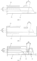
- a display substrate is provided according to an embodiment of the present disclosure, which includes: a base substrate, a display component 110 on the base substrate, and an encapsulation layer 120 covering the display component 110.
- the display component 110 in this embodiment mainly refers to a structure or a functional film layer including, but not limited to, a thin film transistor (TFT) structure, an anode, a cathode, and a light-emitting layer.
- the light-emitting layer may further include a hole transport layer (HTL), an electro luminescent (EL) layer 111, an electron transport layer (ETL).
- HTL hole transport layer
- EL electro luminescent
- ETL electron transport layer
- the above display component 110 may adopt a device structure in the related technologies or other device structures that can be used for displaying or emitting light, which are not further limited and described herein.
- the encapsulation layer 120 may include an organic layer 122 and inorganic layers 121 and 123 that are stacked.
- the encapsulation layer 120 at least includes a first inorganic layer 121, the organic layer 122 and a second inorganic layer 123 that are sequentially stacked.
- the organic layer 122 may adopt an organic ink, and may be formed by an inkjet printing method or other suitable methods that can be used to manufacture the encapsulation layer 120.
- the display substrate further includes a detection capacitor 130 located in a peripheral area of the display substrate.
- a first electrode plate 131 of the detection capacitor 130 is formed on a side of the encapsulation layer 120 close to the base substrate, and a second electrode plate 132 of the detection capacitor 130 is formed on a side of the encapsulation layer 120 far away from the base substrate.
- the peripheral region of the display substrate as shown in FIG. 6 and FIG. 7 refers to an edge position between an effective display area (AA) 160 of the display substrate and a frame 170 of the display substrate.
- the detection capacitor 130 is arranged in the peripheral region, and is configured to determine whether an organic layer in the encapsulation layer of the display substrate overflows to the peripheral region.
- the detection capacitor 130 is provided to detect whether an overflow phenomenon occurs to the organic layer 122 of the encapsulation layer 120.
- the detection capacitor 130 includes the first electrode plate 131 and the second electrode plate 132, and the first electrode plate 131 and the second electrode plate 132 are respectively arranged on two sides of the encapsulation layer 120 at the peripheral region of the display substrate.
- the substance between the first electrode plate 131 and the second electrode plate 132 is an inorganic material of the encapsulation layer 120.
- the substance between the first electrode plate 131 and the second electrode plate 132 is an organic material and an inorganic material of the encapsulation layer 120; and further, if oxygen and water have intruded along the overflow channel, the substance between the first electrode plate 131 and the second electrode plate 132 further includes the water and the oxygen.
- the substance located between the first electrode plate 131 and the second electrode plate 132 serves as an electrolyte of the detection capacitor 130.
- the change of the electrolyte may cause a capacitance between the first electrode plate 131 and the second electrode plate 132 to change.
- a display substrate that is determined to have no overflow phenomenon in the organic layer 122 may be selected, and a capacitance value of the detection capacitor 130 is measured as a reference capacitance value under a normal condition; or in a case that electrolytes between the first electrode plate 131 and the second electrode plate 132 are an inorganic material of the encapsulation layer 120, a capacitance value of the detection capacitor 130 is obtained by theoretical calculation and is taken as a reference capacitance value.
- the organic layer 122 of the display substrate has an overflow phenomenon; and when it is detected that a difference between a capacitance value of a detection capacitor 130 of a certain display substrate and the reference capacitance value is within an allowable range (for example, less than or equal to a threshold value), the display substrate may be deemed in a normal state.
- a detection capacitor 130 is provided on the edge of the encapsulation layer 120.
- the electrolytes between the first electrode plate 131 and the second electrode plate 132 are inorganic materials of the encapsulation layer 120. If the organic layer 122 overflows, the electrolytes between the first electrode plate 131 and the second electrode plate 132 are the organic material and inorganic material of the encapsulation layer 120, which results in a deviation in the capacitance value between the first electrode plate 131 and the second electrode plate 132, as compared with the reference capacitance value, so that the overflow of the organic layer 122 can be detected.
- the first electrode plate 131 may be an electrode plate separately formed through an additional patterning process.
- the first electrode plate 131 is manufactured before the encapsulation layer 120 is formed.
- the first electrode plate 131 is formed with a same material and on a same layer as a source-drain metal layer pattern or an anode layer of the display component 110, that is, forming a pattern of the first electrode plate 131 when forming the drain-source metal layer or the anode layer pattern of the display component 110.
- the production process can be simplified, as compared to manufacturing the first electrode plate 131 exclusively through an additional patterning process.
- the second electrode plate 132 in an embodiment may also be an electrode plate separately formed through an additional patterning process. For example, after the encapsulation layer 120 is formed, the second electrode plate 132 is formed at a position corresponding to the first electrode plate 131, so that a position where the organic layer 122 may overflow is between the first electrode plate 131 and the second electrode plate 132.
- the first electrode plate 131 and the second electrode plate 132 of the detection capacitor 130 may be made of a suitable conductive material, such as a capacitor electrode plate made of a metal material.
- the first electrode plate 131 and the second electrode plate 132 may be electrode plates made of aluminum.
- the above technical solution is applied to a display substrate with a FMLOC structure.
- the display substrate with the FMLOC structure refers to a display substrate further provided with a touch sensor on a thin film encapsulation layer (TFE) 120.
- TFE thin film encapsulation layer
- the touch sensor of the display substrate further includes a touch electrode 150 on the encapsulation layer 120, and the second electrode plate 132 of the detection capacitor 130 may be arranged on the same layer and made of the same material as the touch electrode 150.
- the pattern of the second electrode plate 132 may be formed at the same time, which can also have the effect of simplifying the production process.
- a material of the second electrode plate 132 is the same as that of the touch electrode 150, which, for example, may be a Ti-Al-Ti (titanium-aluminum-titanium) metal laminated structure.
- Each inorganic layer is usually made of an oxide of silicon.
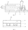
- the touch electrode 150 may be configured to include first electrodes 211 and second electrodes 221, where an extending direction of the first electrodes 211 is perpendicular to an extending direction of the second electrodes 221, and touch detection is achieved through a mutual capacitance structure formed between the first electrodes and the second electrodes.
- metal bridges 222 are configured to connect the second electrodes 221 that are separated apart from each other in the lateral direction (a horizontal direction shown in FIG. 5 ).
- the first electrodes 211 and the second electrodes 221 may be disposed on the same layer.
- At least one of the first electrode 211 or the second electrode 221 may be a structure of a Ti metal layer, an Al metal layer and the Ti metal layer that are laminated.
- the touch electrode 150 may further include passivation layers 210 and 220 that are disposed on both sides of the electrode layer, respectively.
- the second electrode plate 132 may be arranged in the same layer and made of the same material as the first electrodes 211, or may be arranged in the same layer and made of the same material as the metal bridges 222.
- a blocking structure is provided at the edge of the encapsulation layer. It should be appreciated that the closer to the edge of the encapsulation layer 120 is, the smaller the thickness of each inorganic layer is, and it is easier for the organic layer 122 to overflow. In general, the blocking structure is disposed at the edge of the encapsulation layer 120.
- the display substrate in an embodiment further includes a first blocking structure 141 and a second blocking structure 142 located at the edge of the encapsulation layer 120.
- an orthographic projection of the detection capacitor 130 onto the base substrate is between the first blocking structure 141 and the second blocking structure 142.
- the above configuration that the orthographic projection of the detection capacitor 130 onto the base substrate is between the first blocking structure 141 and the second blocking structure 142 helps to provide reliable auxiliary determination when determining the encapsulation quality of the display substrate.
- the orthographic projection of the detection capacitor 130 onto the base substrate may also be located between the effective display area (AA) 160 of the display substrate and the above first blocking structure 141; or the orthographic projection of the detection capacitor 130 onto the base substrate may also be located between the frame 170 of the display substrate and the above second blocking structure 142.
- a position of the detection capacitor 130 arranged in the peripheral region of the base substrate can be designed according to actual needs, which is not specifically limited in the present disclosure.
- the possibility that the organic layer 122 overflows can be reduced.
- the electrolytes between the first electrode plate 131 and the second electrode plate 132 include the inorganic material of the encapsulation layer 120.
- the electrolytes between the first electrode plate 131 and the second electrode plate 132 include an organic material of the encapsulation layer 120.
- a difference between a capacitance value of the detection capacitor 130 between the first blocking structure 141 and the second blocking structure 142 and a predetermined reference capacitance value exceeds a threshold value, it may be considered that the organic layer 122 overflows, and it can be considered that the difference is not caused by other interference factors or errors, which can improve the accuracy and reliability of detection results.
- the detection capacitor 130 is disposed between the effective display area (AA area) 160 and the frame 170.
- the detection capacitor 130 may be disposed between the first blocking structure 141 and the second blocking structure 142.
- each detection capacitor 130 may be arranged at intervals along the edge of the encapsulation layer 120. For example, each detection capacitor 130 is disposed at a certain distance from an adjacent detection capacitor to detect whether the organic layer 122 overflows.
- only one detection capacitor 130 may be provided.
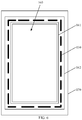
- the detection capacitor 130 has a ring shape, and the detection capacitor 130 surrounds the encapsulation layer 120 along an edge of the encapsulation layer 120.
- the first electrode plate 131 in this embodiment is disposed along the edge of the encapsulation layer 120 and surrounds the encapsulation layer.
- the first electrode plate 131 is actually a ring-shaped plate structure as a whole, and the second electrode plate 132 is arranged at a position corresponding to the first electrode plate 131, so that the above-mentioned detection capacitor 130 is formed between the first electrode plate 131 and the second electrode plate 132.
- An embodiment of the present disclosure further provides a display panel including the display substrate according to any of the above embodiments. Since the display panel in this embodiment includes the display substrate according to any of the above embodiments, at least all the technical effects described above can be achieved, and details are not described herein again.
- An embodiment of the present disclosure further provides a display device including the above display panel. Therefore, at least all the technical effects mentioned above can also be achieved, which are not be repeated herein.
- the display device may include at least one of: a mobile phone, a tablet computer, an e-book reader, an MP3 player, an MP4 player, a digital camera, a laptop portable computer, a vehicle-mounted computer, a desktop computer, a set-top box, a smart television (TV), or a wearable device.
- the present disclosure further provides a method for manufacturing a display substrate.
- the display substrate includes a base substrate and a display component formed on the base substrate, and the manufacturing method includes:
- any display substrate in the above embodiments is given as an example, and in this embodiment, for the step of forming the encapsulation layer 120, any steps that can be used to form the encapsulation layer 120 can be referred to, which is not further limited herein.
- the first electrode plate 131 of the detection capacitor 130 is formed before the encapsulation layer 120 is formed, and the second electrode plate 132 of the detection capacitor 130 is formed after the encapsulation layer 120 is formed.
- the first electrode plate 131 and the second electrode plate 132 are located at edges of the encapsulation layer 120. During implementation, a position of the first electrode plate 131 is determined according to a position where the encapsulation layer 120 needs to be formed, and a pattern of the first electrode plate 131 is formed at the position. After the encapsulation layer 120 is formed, a pattern of the second electrode plate 132 is further formed. Positions and shapes of the first electrode plate 131 and the second electrode plate 132 should correspond to each other, so that a detection capacitor 130 is formed between the first electrode plate 131 and the second electrode plate 132.
- the organic layer 122 does not overflow, inorganic materials are between the first electrode plate 131 and the second electrode plate 132. If the organic layer 122 overflows, organic materials and inorganic materials are between the first electrode plate 131 and the second electrode plate 132, which may result in a change of a capacitance between the first electrode plate 131 and the second electrode plate 132. Therefore, the overflow of the organic layer 122 can be detected.
- the first electrode plate 131 and the second electrode plate 132 are disposed in such a manner that orthographic projections of the first electrode plate 131 and the second electrode plate 132 onto the base substrate are between the first blocking structure 141 and the second blocking structure 142.
- the possibility that the organic layer 122 overflows can be reduced.
- the organic layer 122 does not overflow, a material of the organic layer 122, water and oxygen do not exist in a region between the first blocking structure 141 and the second blocking structure 142.
- a difference between a capacitance value of the detection capacitor 130 between the first blocking structure 141 and the second blocking structure 142 and a predetermined reference capacitance value exceeds a threshold value, it may be considered that the organic layer 122 overflows, and it can be considered that the difference is not caused by other interference factors or errors, which can improve the accuracy and reliability of the detection results.
- the step of forming the first electrode plate 131 of the detection capacitor 130 includes: forming the first electrode plate 131 and the source-drain metal layer pattern of the display component 110 at a same time through one patterning process; or forming the first electrode plate 131 and the anode layer of the display component 110 at a same time through one patterning process.
- the step of forming the second electrode plate 132 of the detection capacitor 130 includes: forming the second electrode plate 132 and the touch electrode 150 at a same time through one patterning process.
- the first electrode plate 131 and the second electrode plate 132 may be formed separately, and may also be formed respectively through a single patterning process when forming the source-drain metal layer pattern or the anode layer, and through a single patterning process when forming the touch electrode 150, which is good to simplify production processes.
Landscapes
- Engineering & Computer Science (AREA)
- Theoretical Computer Science (AREA)
- General Engineering & Computer Science (AREA)
- Physics & Mathematics (AREA)
- General Physics & Mathematics (AREA)
- Human Computer Interaction (AREA)
- Chemical & Material Sciences (AREA)
- Inorganic Chemistry (AREA)
- Microelectronics & Electronic Packaging (AREA)
- Manufacturing & Machinery (AREA)
- Optics & Photonics (AREA)
- Geometry (AREA)
- Electroluminescent Light Sources (AREA)
- Devices For Indicating Variable Information By Combining Individual Elements (AREA)
Applications Claiming Priority (2)
| Application Number | Priority Date | Filing Date | Title |
|---|---|---|---|
| CN201810980319.3A CN109119445B (zh) | 2018-08-27 | 2018-08-27 | 一种显示基板及其制作方法、显示面板和显示装置 |
| PCT/CN2019/102752 WO2020043079A1 (fr) | 2018-08-27 | 2019-08-27 | Substrat d'affichage et son procédé de fabrication, panneau d'affichage et appareil d'affichage |
Publications (3)
| Publication Number | Publication Date |
|---|---|
| EP3846213A1 true EP3846213A1 (fr) | 2021-07-07 |
| EP3846213A4 EP3846213A4 (fr) | 2022-05-18 |
| EP3846213B1 EP3846213B1 (fr) | 2024-02-14 |
Family
ID=64860180
Family Applications (1)
| Application Number | Title | Priority Date | Filing Date |
|---|---|---|---|
| EP19855551.8A Active EP3846213B1 (fr) | 2018-08-27 | 2019-08-27 | Substrat d'affichage et son procédé de fabrication, panneau d'affichage et appareil d'affichage |
Country Status (4)
| Country | Link |
|---|---|
| US (1) | US11367758B2 (fr) |
| EP (1) | EP3846213B1 (fr) |
| CN (1) | CN109119445B (fr) |
| WO (1) | WO2020043079A1 (fr) |
Families Citing this family (6)
| Publication number | Priority date | Publication date | Assignee | Title |
|---|---|---|---|---|
| CN109119445B (zh) | 2018-08-27 | 2021-09-14 | 京东方科技集团股份有限公司 | 一种显示基板及其制作方法、显示面板和显示装置 |
| KR102724230B1 (ko) * | 2018-12-03 | 2024-11-01 | 삼성디스플레이 주식회사 | 유기 발광 표시 장치 |
| CN109786581B (zh) * | 2019-02-28 | 2021-09-24 | 昆山国显光电有限公司 | 显示面板和显示面板的制备方法 |
| CN111584552A (zh) * | 2020-05-06 | 2020-08-25 | 华为技术有限公司 | 显示面板、显示屏和电子设备 |
| CN112186017B (zh) * | 2020-09-30 | 2022-12-02 | 京东方科技集团股份有限公司 | 显示面板及制作方法、显示设备 |
| EP4459445A4 (fr) | 2022-08-29 | 2025-07-02 | Boe Technology Group Co Ltd | Écran d'affichage et dispositif d'affichage |
Family Cites Families (15)
| Publication number | Priority date | Publication date | Assignee | Title |
|---|---|---|---|---|
| KR20150017991A (ko) | 2013-08-08 | 2015-02-23 | 삼성디스플레이 주식회사 | 봉지막을 구비하는 표시장치 및 봉지막 검사 방법 |
| JP2015056335A (ja) * | 2013-09-13 | 2015-03-23 | セイコーエプソン株式会社 | 電気光学装置、電子機器及び電気光学装置の製造方法 |
| KR102162912B1 (ko) * | 2013-12-06 | 2020-10-07 | 엘지디스플레이 주식회사 | 터치패널을 구비한 유기전계 발광장치 및 그 제조방법 |
| KR102362189B1 (ko) | 2015-04-16 | 2022-02-11 | 삼성디스플레이 주식회사 | 유기 발광 표시 장치 |
| CN104900681B (zh) | 2015-06-09 | 2019-02-05 | 上海天马有机发光显示技术有限公司 | 有机发光显示面板及其形成方法 |
| CN105895827B (zh) * | 2016-06-28 | 2017-11-07 | 京东方科技集团股份有限公司 | 一种有机发光显示器件及其封装方法、显示装置 |
| KR101979444B1 (ko) | 2016-07-29 | 2019-05-17 | 삼성디스플레이 주식회사 | 표시장치 |
| KR102553910B1 (ko) * | 2016-08-31 | 2023-07-07 | 엘지디스플레이 주식회사 | 표시장치와 그의 검사방법 |
| KR102671040B1 (ko) * | 2016-10-10 | 2024-06-03 | 삼성디스플레이 주식회사 | 디스플레이 장치 |
| CN106505089B (zh) * | 2016-10-31 | 2019-11-05 | 上海天马微电子有限公司 | 显示器件 |
| KR102793060B1 (ko) | 2016-12-16 | 2025-04-08 | 엘지디스플레이 주식회사 | 표시 장치 및 그 제조 방법 |
| CN107491209B (zh) * | 2017-08-11 | 2020-10-09 | 上海天马微电子有限公司 | 触控显示装置 |
| CN107742635B (zh) | 2017-09-27 | 2020-07-03 | 京东方科技集团股份有限公司 | 一种显示面板及其制备方法 |
| CN108061983B (zh) * | 2018-01-03 | 2020-07-14 | 京东方科技集团股份有限公司 | 配向膜边界到显示区的距离的测量方法及测量装置 |
| CN109119445B (zh) * | 2018-08-27 | 2021-09-14 | 京东方科技集团股份有限公司 | 一种显示基板及其制作方法、显示面板和显示装置 |
-
2018
- 2018-08-27 CN CN201810980319.3A patent/CN109119445B/zh active Active
-
2019
- 2019-08-27 EP EP19855551.8A patent/EP3846213B1/fr active Active
- 2019-08-27 US US16/643,362 patent/US11367758B2/en active Active
- 2019-08-27 WO PCT/CN2019/102752 patent/WO2020043079A1/fr not_active Ceased
Also Published As
| Publication number | Publication date |
|---|---|
| EP3846213A4 (fr) | 2022-05-18 |
| EP3846213B1 (fr) | 2024-02-14 |
| US20210074771A1 (en) | 2021-03-11 |
| US11367758B2 (en) | 2022-06-21 |
| CN109119445B (zh) | 2021-09-14 |
| WO2020043079A1 (fr) | 2020-03-05 |
| CN109119445A (zh) | 2019-01-01 |
Similar Documents
| Publication | Publication Date | Title |
|---|---|---|
| US11367758B2 (en) | Display substrate and method for manufacturing the same, display panel and display device | |
| US12010905B2 (en) | Display apparatus including a substrate having a hole | |
| US10872932B2 (en) | Organic electroluminescent display substrate, method for manufacturing the same and display device | |
| US11563076B2 (en) | Display panel and preparation method thereof and display apparatus | |
| US10761660B2 (en) | Touch display device having touch display panel capable of preventing short circuit of adjacent tough lines | |
| US11417719B2 (en) | Organic light-emitting diode display panel with anode layer on signal trace in non-display area | |
| US11882716B2 (en) | Display panel, method for manufacturing same, and display apparatus | |
| US20210359069A1 (en) | Display substrate and display device | |
| US20150333115A1 (en) | Flexible display substrate and a manufacturing method thereof, as well as a flexible display device | |
| US10553814B2 (en) | Array substrate, display panel, display device, method for manufacturing array substrate and method for manufacturing display panel | |
| US20150261365A1 (en) | Display device | |
| US10180742B2 (en) | Display panel, method for fabricating the same, and display apparatus | |
| US10243027B2 (en) | Display panel, fabricating method thereof, and display apparatus | |
| US12501812B2 (en) | Displaying base plate and displaying device | |
| US20250185465A1 (en) | Display panel, display apparatus, and method for manufacturing display panel | |
| US20200066813A1 (en) | Electroluminescent display panel, manufacturing method thereof and display device | |
| US10220607B2 (en) | Screen mask assembly | |
| US20170194600A1 (en) | Packaging method of oled device, package structure and display apparatus | |
| CN115802795B (zh) | 一种显示面板及显示装置 | |
| US11437546B2 (en) | Display panel and display module | |
| US20230165072A1 (en) | Display panel and manufacturing method thereof, and display device | |
| US20240049567A1 (en) | Oled display panel and electronic device | |
| US11195900B2 (en) | Array substrate with protrusion patterns and method of fabricating same | |
| KR20220072947A (ko) | 표시 장치 및 이의 제조 방법 | |
| CN110620105B (zh) | 阵列基板及其制造方法、阵列基板的图案偏移的检测方法 |
Legal Events
| Date | Code | Title | Description |
|---|---|---|---|
| STAA | Information on the status of an ep patent application or granted ep patent |
Free format text: STATUS: THE INTERNATIONAL PUBLICATION HAS BEEN MADE |
|
| STAA | Information on the status of an ep patent application or granted ep patent |
Free format text: STATUS: REQUEST FOR EXAMINATION WAS MADE |
|
| PUAI | Public reference made under article 153(3) epc to a published international application that has entered the european phase |
Free format text: ORIGINAL CODE: 0009012 |
|
| 17P | Request for examination filed |
Effective date: 20200309 |
|
| AK | Designated contracting states |
Kind code of ref document: A1 Designated state(s): AL AT BE BG CH CY CZ DE DK EE ES FI FR GB GR HR HU IE IS IT LI LT LU LV MC MK MT NL NO PL PT RO RS SE SI SK SM TR |
|
| DAV | Request for validation of the european patent (deleted) | ||
| DAX | Request for extension of the european patent (deleted) | ||
| A4 | Supplementary search report drawn up and despatched |
Effective date: 20220420 |
|
| RIC1 | Information provided on ipc code assigned before grant |
Ipc: H01L 51/56 20060101ALI20220412BHEP Ipc: H01L 51/52 20060101ALI20220412BHEP Ipc: H01L 21/66 20060101ALI20220412BHEP Ipc: H01L 27/32 20060101AFI20220412BHEP |
|
| REG | Reference to a national code |
Ref legal event code: R079 Ipc: H10K0059121000 Ref country code: DE Ref document number: 602019046663 Country of ref document: DE Free format text: PREVIOUS MAIN CLASS: H01L0027320000 |
|
| RIC1 | Information provided on ipc code assigned before grant |
Ipc: H10K 59/40 20230101ALI20230921BHEP Ipc: H10K 59/80 20230101ALI20230921BHEP Ipc: H10K 59/121 20230101AFI20230921BHEP |
|
| GRAP | Despatch of communication of intention to grant a patent |
Free format text: ORIGINAL CODE: EPIDOSNIGR1 |
|
| STAA | Information on the status of an ep patent application or granted ep patent |
Free format text: STATUS: GRANT OF PATENT IS INTENDED |
|
| RIC1 | Information provided on ipc code assigned before grant |
Ipc: G06F 3/044 20060101ALI20231027BHEP Ipc: G06F 3/041 20060101ALI20231027BHEP Ipc: H10K 59/40 20230101ALI20231027BHEP Ipc: H10K 59/80 20230101ALI20231027BHEP Ipc: H10K 59/121 20230101AFI20231027BHEP |
|
| INTG | Intention to grant announced |
Effective date: 20231117 |
|
| GRAS | Grant fee paid |
Free format text: ORIGINAL CODE: EPIDOSNIGR3 |
|
| GRAA | (expected) grant |
Free format text: ORIGINAL CODE: 0009210 |
|
| STAA | Information on the status of an ep patent application or granted ep patent |
Free format text: STATUS: THE PATENT HAS BEEN GRANTED |
|
| AK | Designated contracting states |
Kind code of ref document: B1 Designated state(s): AL AT BE BG CH CY CZ DE DK EE ES FI FR GB GR HR HU IE IS IT LI LT LU LV MC MK MT NL NO PL PT RO RS SE SI SK SM TR |
|
| REG | Reference to a national code |
Ref country code: GB Ref legal event code: FG4D |
|
| REG | Reference to a national code |
Ref country code: CH Ref legal event code: EP |
|
| REG | Reference to a national code |
Ref country code: DE Ref legal event code: R096 Ref document number: 602019046663 Country of ref document: DE |
|
| REG | Reference to a national code |
Ref country code: IE Ref legal event code: FG4D |
|
| REG | Reference to a national code |
Ref country code: LT Ref legal event code: MG9D |
|
| REG | Reference to a national code |
Ref country code: NL Ref legal event code: MP Effective date: 20240214 |
|
| PG25 | Lapsed in a contracting state [announced via postgrant information from national office to epo] |
Ref country code: IS Free format text: LAPSE BECAUSE OF FAILURE TO SUBMIT A TRANSLATION OF THE DESCRIPTION OR TO PAY THE FEE WITHIN THE PRESCRIBED TIME-LIMIT Effective date: 20240614 |
|
| PG25 | Lapsed in a contracting state [announced via postgrant information from national office to epo] |
Ref country code: LT Free format text: LAPSE BECAUSE OF FAILURE TO SUBMIT A TRANSLATION OF THE DESCRIPTION OR TO PAY THE FEE WITHIN THE PRESCRIBED TIME-LIMIT Effective date: 20240214 |
|
| PG25 | Lapsed in a contracting state [announced via postgrant information from national office to epo] |
Ref country code: GR Free format text: LAPSE BECAUSE OF FAILURE TO SUBMIT A TRANSLATION OF THE DESCRIPTION OR TO PAY THE FEE WITHIN THE PRESCRIBED TIME-LIMIT Effective date: 20240515 |
|
| REG | Reference to a national code |
Ref country code: AT Ref legal event code: MK05 Ref document number: 1658204 Country of ref document: AT Kind code of ref document: T Effective date: 20240214 |
|
| PG25 | Lapsed in a contracting state [announced via postgrant information from national office to epo] |
Ref country code: RS Free format text: LAPSE BECAUSE OF FAILURE TO SUBMIT A TRANSLATION OF THE DESCRIPTION OR TO PAY THE FEE WITHIN THE PRESCRIBED TIME-LIMIT Effective date: 20240514 Ref country code: NL Free format text: LAPSE BECAUSE OF FAILURE TO SUBMIT A TRANSLATION OF THE DESCRIPTION OR TO PAY THE FEE WITHIN THE PRESCRIBED TIME-LIMIT Effective date: 20240214 Ref country code: HR Free format text: LAPSE BECAUSE OF FAILURE TO SUBMIT A TRANSLATION OF THE DESCRIPTION OR TO PAY THE FEE WITHIN THE PRESCRIBED TIME-LIMIT Effective date: 20240214 |
|
| PG25 | Lapsed in a contracting state [announced via postgrant information from national office to epo] |
Ref country code: ES Free format text: LAPSE BECAUSE OF FAILURE TO SUBMIT A TRANSLATION OF THE DESCRIPTION OR TO PAY THE FEE WITHIN THE PRESCRIBED TIME-LIMIT Effective date: 20240214 |
|
| PG25 | Lapsed in a contracting state [announced via postgrant information from national office to epo] |
Ref country code: AT Free format text: LAPSE BECAUSE OF FAILURE TO SUBMIT A TRANSLATION OF THE DESCRIPTION OR TO PAY THE FEE WITHIN THE PRESCRIBED TIME-LIMIT Effective date: 20240214 |
|
| PG25 | Lapsed in a contracting state [announced via postgrant information from national office to epo] |
Ref country code: RS Free format text: LAPSE BECAUSE OF FAILURE TO SUBMIT A TRANSLATION OF THE DESCRIPTION OR TO PAY THE FEE WITHIN THE PRESCRIBED TIME-LIMIT Effective date: 20240514 Ref country code: NO Free format text: LAPSE BECAUSE OF FAILURE TO SUBMIT A TRANSLATION OF THE DESCRIPTION OR TO PAY THE FEE WITHIN THE PRESCRIBED TIME-LIMIT Effective date: 20240514 Ref country code: NL Free format text: LAPSE BECAUSE OF FAILURE TO SUBMIT A TRANSLATION OF THE DESCRIPTION OR TO PAY THE FEE WITHIN THE PRESCRIBED TIME-LIMIT Effective date: 20240214 Ref country code: LT Free format text: LAPSE BECAUSE OF FAILURE TO SUBMIT A TRANSLATION OF THE DESCRIPTION OR TO PAY THE FEE WITHIN THE PRESCRIBED TIME-LIMIT Effective date: 20240214 Ref country code: IS Free format text: LAPSE BECAUSE OF FAILURE TO SUBMIT A TRANSLATION OF THE DESCRIPTION OR TO PAY THE FEE WITHIN THE PRESCRIBED TIME-LIMIT Effective date: 20240614 Ref country code: HR Free format text: LAPSE BECAUSE OF FAILURE TO SUBMIT A TRANSLATION OF THE DESCRIPTION OR TO PAY THE FEE WITHIN THE PRESCRIBED TIME-LIMIT Effective date: 20240214 Ref country code: GR Free format text: LAPSE BECAUSE OF FAILURE TO SUBMIT A TRANSLATION OF THE DESCRIPTION OR TO PAY THE FEE WITHIN THE PRESCRIBED TIME-LIMIT Effective date: 20240515 Ref country code: FI Free format text: LAPSE BECAUSE OF FAILURE TO SUBMIT A TRANSLATION OF THE DESCRIPTION OR TO PAY THE FEE WITHIN THE PRESCRIBED TIME-LIMIT Effective date: 20240214 Ref country code: ES Free format text: LAPSE BECAUSE OF FAILURE TO SUBMIT A TRANSLATION OF THE DESCRIPTION OR TO PAY THE FEE WITHIN THE PRESCRIBED TIME-LIMIT Effective date: 20240214 Ref country code: BG Free format text: LAPSE BECAUSE OF FAILURE TO SUBMIT A TRANSLATION OF THE DESCRIPTION OR TO PAY THE FEE WITHIN THE PRESCRIBED TIME-LIMIT Effective date: 20240214 Ref country code: AT Free format text: LAPSE BECAUSE OF FAILURE TO SUBMIT A TRANSLATION OF THE DESCRIPTION OR TO PAY THE FEE WITHIN THE PRESCRIBED TIME-LIMIT Effective date: 20240214 |
|
| PG25 | Lapsed in a contracting state [announced via postgrant information from national office to epo] |
Ref country code: PT Free format text: LAPSE BECAUSE OF FAILURE TO SUBMIT A TRANSLATION OF THE DESCRIPTION OR TO PAY THE FEE WITHIN THE PRESCRIBED TIME-LIMIT Effective date: 20240614 Ref country code: PL Free format text: LAPSE BECAUSE OF FAILURE TO SUBMIT A TRANSLATION OF THE DESCRIPTION OR TO PAY THE FEE WITHIN THE PRESCRIBED TIME-LIMIT Effective date: 20240214 |
|
| PG25 | Lapsed in a contracting state [announced via postgrant information from national office to epo] |
Ref country code: SE Free format text: LAPSE BECAUSE OF FAILURE TO SUBMIT A TRANSLATION OF THE DESCRIPTION OR TO PAY THE FEE WITHIN THE PRESCRIBED TIME-LIMIT Effective date: 20240214 Ref country code: PT Free format text: LAPSE BECAUSE OF FAILURE TO SUBMIT A TRANSLATION OF THE DESCRIPTION OR TO PAY THE FEE WITHIN THE PRESCRIBED TIME-LIMIT Effective date: 20240614 Ref country code: PL Free format text: LAPSE BECAUSE OF FAILURE TO SUBMIT A TRANSLATION OF THE DESCRIPTION OR TO PAY THE FEE WITHIN THE PRESCRIBED TIME-LIMIT Effective date: 20240214 Ref country code: LV Free format text: LAPSE BECAUSE OF FAILURE TO SUBMIT A TRANSLATION OF THE DESCRIPTION OR TO PAY THE FEE WITHIN THE PRESCRIBED TIME-LIMIT Effective date: 20240214 |
|
| PG25 | Lapsed in a contracting state [announced via postgrant information from national office to epo] |
Ref country code: DK Free format text: LAPSE BECAUSE OF FAILURE TO SUBMIT A TRANSLATION OF THE DESCRIPTION OR TO PAY THE FEE WITHIN THE PRESCRIBED TIME-LIMIT Effective date: 20240214 |
|
| PG25 | Lapsed in a contracting state [announced via postgrant information from national office to epo] |
Ref country code: SM Free format text: LAPSE BECAUSE OF FAILURE TO SUBMIT A TRANSLATION OF THE DESCRIPTION OR TO PAY THE FEE WITHIN THE PRESCRIBED TIME-LIMIT Effective date: 20240214 |
|
| PG25 | Lapsed in a contracting state [announced via postgrant information from national office to epo] |
Ref country code: CZ Free format text: LAPSE BECAUSE OF FAILURE TO SUBMIT A TRANSLATION OF THE DESCRIPTION OR TO PAY THE FEE WITHIN THE PRESCRIBED TIME-LIMIT Effective date: 20240214 Ref country code: EE Free format text: LAPSE BECAUSE OF FAILURE TO SUBMIT A TRANSLATION OF THE DESCRIPTION OR TO PAY THE FEE WITHIN THE PRESCRIBED TIME-LIMIT Effective date: 20240214 |
|
| PG25 | Lapsed in a contracting state [announced via postgrant information from national office to epo] |
Ref country code: SK Free format text: LAPSE BECAUSE OF FAILURE TO SUBMIT A TRANSLATION OF THE DESCRIPTION OR TO PAY THE FEE WITHIN THE PRESCRIBED TIME-LIMIT Effective date: 20240214 |
|
| PG25 | Lapsed in a contracting state [announced via postgrant information from national office to epo] |
Ref country code: SM Free format text: LAPSE BECAUSE OF FAILURE TO SUBMIT A TRANSLATION OF THE DESCRIPTION OR TO PAY THE FEE WITHIN THE PRESCRIBED TIME-LIMIT Effective date: 20240214 Ref country code: SK Free format text: LAPSE BECAUSE OF FAILURE TO SUBMIT A TRANSLATION OF THE DESCRIPTION OR TO PAY THE FEE WITHIN THE PRESCRIBED TIME-LIMIT Effective date: 20240214 Ref country code: RO Free format text: LAPSE BECAUSE OF FAILURE TO SUBMIT A TRANSLATION OF THE DESCRIPTION OR TO PAY THE FEE WITHIN THE PRESCRIBED TIME-LIMIT Effective date: 20240214 Ref country code: EE Free format text: LAPSE BECAUSE OF FAILURE TO SUBMIT A TRANSLATION OF THE DESCRIPTION OR TO PAY THE FEE WITHIN THE PRESCRIBED TIME-LIMIT Effective date: 20240214 Ref country code: DK Free format text: LAPSE BECAUSE OF FAILURE TO SUBMIT A TRANSLATION OF THE DESCRIPTION OR TO PAY THE FEE WITHIN THE PRESCRIBED TIME-LIMIT Effective date: 20240214 Ref country code: CZ Free format text: LAPSE BECAUSE OF FAILURE TO SUBMIT A TRANSLATION OF THE DESCRIPTION OR TO PAY THE FEE WITHIN THE PRESCRIBED TIME-LIMIT Effective date: 20240214 |
|
| REG | Reference to a national code |
Ref country code: DE Ref legal event code: R097 Ref document number: 602019046663 Country of ref document: DE |
|
| PG25 | Lapsed in a contracting state [announced via postgrant information from national office to epo] |
Ref country code: IT Free format text: LAPSE BECAUSE OF FAILURE TO SUBMIT A TRANSLATION OF THE DESCRIPTION OR TO PAY THE FEE WITHIN THE PRESCRIBED TIME-LIMIT Effective date: 20240214 |
|
| PLBE | No opposition filed within time limit |
Free format text: ORIGINAL CODE: 0009261 |
|
| STAA | Information on the status of an ep patent application or granted ep patent |
Free format text: STATUS: NO OPPOSITION FILED WITHIN TIME LIMIT |
|
| PG25 | Lapsed in a contracting state [announced via postgrant information from national office to epo] |
Ref country code: IT Free format text: LAPSE BECAUSE OF FAILURE TO SUBMIT A TRANSLATION OF THE DESCRIPTION OR TO PAY THE FEE WITHIN THE PRESCRIBED TIME-LIMIT Effective date: 20240214 |
|
| 26N | No opposition filed |
Effective date: 20241115 |
|
| REG | Reference to a national code |
Ref country code: CH Ref legal event code: PL |
|
| PG25 | Lapsed in a contracting state [announced via postgrant information from national office to epo] |
Ref country code: LU Free format text: LAPSE BECAUSE OF NON-PAYMENT OF DUE FEES Effective date: 20240827 |
|
| PG25 | Lapsed in a contracting state [announced via postgrant information from national office to epo] |
Ref country code: SI Free format text: LAPSE BECAUSE OF FAILURE TO SUBMIT A TRANSLATION OF THE DESCRIPTION OR TO PAY THE FEE WITHIN THE PRESCRIBED TIME-LIMIT Effective date: 20240214 Ref country code: CH Free format text: LAPSE BECAUSE OF NON-PAYMENT OF DUE FEES Effective date: 20240831 Ref country code: MC Free format text: LAPSE BECAUSE OF FAILURE TO SUBMIT A TRANSLATION OF THE DESCRIPTION OR TO PAY THE FEE WITHIN THE PRESCRIBED TIME-LIMIT Effective date: 20240214 |
|
| REG | Reference to a national code |
Ref country code: BE Ref legal event code: MM Effective date: 20240831 |
|
| PG25 | Lapsed in a contracting state [announced via postgrant information from national office to epo] |
Ref country code: BE Free format text: LAPSE BECAUSE OF NON-PAYMENT OF DUE FEES Effective date: 20240831 |
|
| PG25 | Lapsed in a contracting state [announced via postgrant information from national office to epo] |
Ref country code: FR Free format text: LAPSE BECAUSE OF NON-PAYMENT OF DUE FEES Effective date: 20240831 |
|
| PG25 | Lapsed in a contracting state [announced via postgrant information from national office to epo] |
Ref country code: IE Free format text: LAPSE BECAUSE OF NON-PAYMENT OF DUE FEES Effective date: 20240827 |
|
| PGFP | Annual fee paid to national office [announced via postgrant information from national office to epo] |
Ref country code: DE Payment date: 20250820 Year of fee payment: 7 |
|
| PGFP | Annual fee paid to national office [announced via postgrant information from national office to epo] |
Ref country code: GB Payment date: 20250820 Year of fee payment: 7 |
|
| PG25 | Lapsed in a contracting state [announced via postgrant information from national office to epo] |
Ref country code: CY Free format text: LAPSE BECAUSE OF FAILURE TO SUBMIT A TRANSLATION OF THE DESCRIPTION OR TO PAY THE FEE WITHIN THE PRESCRIBED TIME-LIMIT; INVALID AB INITIO Effective date: 20190827 |
|
| PG25 | Lapsed in a contracting state [announced via postgrant information from national office to epo] |
Ref country code: HU Free format text: LAPSE BECAUSE OF FAILURE TO SUBMIT A TRANSLATION OF THE DESCRIPTION OR TO PAY THE FEE WITHIN THE PRESCRIBED TIME-LIMIT; INVALID AB INITIO Effective date: 20190827 |