EP3847533B1 - Module de capteur d'empreinte digitale optique et procédé de fonctionnement d'un module de d'empreinte digitale optique - Google Patents
Module de capteur d'empreinte digitale optique et procédé de fonctionnement d'un module de d'empreinte digitale optique Download PDFInfo
- Publication number
- EP3847533B1 EP3847533B1 EP18932346.2A EP18932346A EP3847533B1 EP 3847533 B1 EP3847533 B1 EP 3847533B1 EP 18932346 A EP18932346 A EP 18932346A EP 3847533 B1 EP3847533 B1 EP 3847533B1
- Authority
- EP
- European Patent Office
- Prior art keywords
- imaging device
- electrically conductive
- image sensor
- biometric imaging
- conductive structure
- Prior art date
- Legal status (The legal status is an assumption and is not a legal conclusion. Google has not performed a legal analysis and makes no representation as to the accuracy of the status listed.)
- Active
Links
Images




Classifications
-
- G—PHYSICS
- G06—COMPUTING OR CALCULATING; COUNTING
- G06F—ELECTRIC DIGITAL DATA PROCESSING
- G06F3/00—Input arrangements for transferring data to be processed into a form capable of being handled by the computer; Output arrangements for transferring data from processing unit to output unit, e.g. interface arrangements
- G06F3/01—Input arrangements or combined input and output arrangements for interaction between user and computer
- G06F3/03—Arrangements for converting the position or the displacement of a member into a coded form
- G06F3/041—Digitisers, e.g. for touch screens or touch pads, characterised by the transducing means
- G06F3/044—Digitisers, e.g. for touch screens or touch pads, characterised by the transducing means by capacitive means
- G06F3/0447—Position sensing using the local deformation of sensor cells
-
- G—PHYSICS
- G06—COMPUTING OR CALCULATING; COUNTING
- G06F—ELECTRIC DIGITAL DATA PROCESSING
- G06F1/00—Details not covered by groups G06F3/00 - G06F13/00 and G06F21/00
- G06F1/16—Constructional details or arrangements
- G06F1/1613—Constructional details or arrangements for portable computers
- G06F1/1626—Constructional details or arrangements for portable computers with a single-body enclosure integrating a flat display, e.g. Personal Digital Assistants [PDAs]
-
- G—PHYSICS
- G06—COMPUTING OR CALCULATING; COUNTING
- G06F—ELECTRIC DIGITAL DATA PROCESSING
- G06F1/00—Details not covered by groups G06F3/00 - G06F13/00 and G06F21/00
- G06F1/16—Constructional details or arrangements
- G06F1/1613—Constructional details or arrangements for portable computers
- G06F1/1633—Constructional details or arrangements of portable computers not specific to the type of enclosures covered by groups G06F1/1615 - G06F1/1626
- G06F1/1637—Details related to the display arrangement, including those related to the mounting of the display in the housing
-
- G—PHYSICS
- G06—COMPUTING OR CALCULATING; COUNTING
- G06F—ELECTRIC DIGITAL DATA PROCESSING
- G06F1/00—Details not covered by groups G06F3/00 - G06F13/00 and G06F21/00
- G06F1/16—Constructional details or arrangements
- G06F1/1613—Constructional details or arrangements for portable computers
- G06F1/1633—Constructional details or arrangements of portable computers not specific to the type of enclosures covered by groups G06F1/1615 - G06F1/1626
- G06F1/1684—Constructional details or arrangements related to integrated I/O peripherals not covered by groups G06F1/1635 - G06F1/1675
-
- G—PHYSICS
- G06—COMPUTING OR CALCULATING; COUNTING
- G06F—ELECTRIC DIGITAL DATA PROCESSING
- G06F3/00—Input arrangements for transferring data to be processed into a form capable of being handled by the computer; Output arrangements for transferring data from processing unit to output unit, e.g. interface arrangements
- G06F3/01—Input arrangements or combined input and output arrangements for interaction between user and computer
- G06F3/03—Arrangements for converting the position or the displacement of a member into a coded form
- G06F3/041—Digitisers, e.g. for touch screens or touch pads, characterised by the transducing means
- G06F3/044—Digitisers, e.g. for touch screens or touch pads, characterised by the transducing means by capacitive means
- G06F3/0445—Digitisers, e.g. for touch screens or touch pads, characterised by the transducing means by capacitive means using two or more layers of sensing electrodes, e.g. using two layers of electrodes separated by a dielectric layer
-
- H—ELECTRICITY
- H03—ELECTRONIC CIRCUITRY
- H03K—PULSE TECHNIQUE
- H03K17/00—Electronic switching or gating, i.e. not by contact-making and –breaking
- H03K17/94—Electronic switching or gating, i.e. not by contact-making and –breaking characterised by the way in which the control signals are generated
- H03K17/96—Touch switches
- H03K17/9625—Touch switches using a force resistance transducer
-
- G—PHYSICS
- G06—COMPUTING OR CALCULATING; COUNTING
- G06F—ELECTRIC DIGITAL DATA PROCESSING
- G06F21/00—Security arrangements for protecting computers, components thereof, programs or data against unauthorised activity
- G06F21/30—Authentication, i.e. establishing the identity or authorisation of security principals
- G06F21/31—User authentication
- G06F21/32—User authentication using biometric data, e.g. fingerprints, iris scans or voiceprints
Definitions
- the present invention relates to an optical fingerprint sensor and to a method for operating an optical fingerprint sensor.
- the invention relates to the integration of an optical fingerprint sensor with a display panel.
- Biometric systems are widely used as means for increasing the convenience and security of personal electronic devices, such as mobile phones etc. Fingerprint sensing systems, in particular, are now included in a large proportion of all newly released consumer electronic devices, such as mobile phones.
- Optical fingerprint sensors have been known for some time and may be a feasible alternative to e.g. capacitive fingerprint sensors in certain applications.
- Optical fingerprint sensors may for example be based on the pinhole imaging principle and/or may employ micro-channels, i.e. collimators or microlenses to focus incoming light onto an image sensor.
- Optical fingerprint sensors in particular have shown promise for display integration where an optical fingerprint sensor can be attached to the bottom side of an at least partially transparent display panel.
- WO 2018/155851 A1 describes an electronic device comprising a biometric sensor disposed in a display. It is further described that a pressure sensor module can be disposed in the surrounding region of the biometric sensor module under the display module in a second printed circuit board.
- an object of the present invention to provide an improved optical biometric imaging device integrated with a display panel.
- the described biometric imaging device is primarily intended for fingerprint recognition, but may also be used to capture other biometric features such as a palmprint and the like.
- an optical biometric imaging device according to claim 1.
- the outer surface of the biometric imaging device can be assumed to be the surface of a display panel under which the image sensor is arranged.
- the image sensor is configured to capture an image of an object such as a finger in contact with the outer surface with sufficient resolution for capturing a fingerprint to be used for identification authentication etc.
- the display panel is arranged on top of and at a distance from the image sensor means that there is no direct contact between the display panel and the image sensor, and furthermore that the distance is selected so that the display panel is allowed to flex a certain amount without making contact with any part of the image sensor.
- the display panel may for example flex as a result of a user pressing down on the display panel during normal use of a device such as a smartphone in which the display panel may be integrated.
- the first electrically conductive structure is separated from the second electrically conductive structure such that the two structures form the plates of a parallel plate capacitor arranged with an insulator therebetween.
- the insulator is here provided by the air gap between the first and second electrically insulating structures, allowing the distance between the structures to change with the flex of the display panel.
- the capacitive readout circuitry is coupled to the first and second electrically conductive structures in order to determine a capacitance therebetween.
- the capacitive readout circuitry may for example be integrated with the image sensor circuitry. However, it is also possible to provide the capacitive readout circuitry as separate circuitry arranged in the vicinity of the image sensor.
- the present invention is based on the realization that it is advantageous to arrange an image sensor of a biometric imaging device separate from the display panel to simplify the manufacturing of the device in which the biometric imaging device is arranged.
- the image sensor when the image sensor is physically separated from the bottom surface of the display panel, the distance between a finger in contact with the outer surface of the display panel and the image sensor may change depending on the amount of force applied to the surface. Accordingly, by forming a capacitor between the bottom surface of the display panel and the image sensor, the distance between the finger and the image sensor can be accurately determined, which in turn allows the image sensor to be adjusted to the distance for a specific image acquisition.
- a further advantage of determining the capacitance as described is that an accidental light touch on the surface can be distinguished from an intentional contact. This may for example be advantageous if the biometric imaging device is in a sleep mode and where a surface touch is used to wake up the device, where it can be ensured that the biometric imaging device and/or the display panel only wakes up if the outer surface is contacted with sufficient force.
- the optical biometric imaging device may further comprise a frame, wherein a cover glass of the display panel is arranged to rest on the frame and the image sensor is arranged within the frame.
- the frame may for example be a rectangular frame encircling an inner volume where the image sensor is located.
- the frame may also consist of several individual sections.
- the cover glass will thus have larger surface area than the active parts of the display panel such that the display panel exhibits a T-shaped cross-section such that the cover glass can be arranged in mechanical contact with the frame.
- the optical biometric imaging device may further comprise a carrier, wherein the photodetector pixel array is arranged on the carrier and the first electrically conductive structure is arranged on the carrier adjacent to the photodetector pixel array.
- the optical biometric imaging device may further comprise a spacer arranged on the carrier adjacent to the first electrically conductive structure.
- the spacer can be used to prevent the bottom surface of the display panel from making contact with the image sensor in case of excessive force on the display panel.
- the spacer may also be configured to prevent the first electrically conductive structure from making contact with the second electrically conductive structure, which could potentially cause damage to the electrically conductive structures and to the capacitance readout circuitry.
- the optical biometric imaging device may further comprise a spacer arranged between the carrier and the first electrically conductive structure.
- the distance between the first electrically conductive structure and the second electrically conductive structure can be easily controlled by controlling the height of the spacer.
- the optical biometric imaging device may comprise a plurality of said first electrically conductive structures. It is thereby possible to determine the distance between the image sensor and the display panel at a plurality of locations.
- the display panel may comprise a plurality of said second electrically conductive structures.
- There may for example be one electrically conductive structure on the display panel for each corresponding electrically conductive structure on the image sensor.
- the deformation of the display panel can be assumed to depend on the location or locations where force is applied and also on the magnitude of the applied force. Thereby, it may for example be possible to determine if one or more objects are in contact with the surface and the size of an object in contact with the surface may also be estimated.
- the frame may comprise a floor portion, thereby forming a U-shaped bracket.
- the frame can thereby be seen as a box having five sides and where the display panel is arranged as a lid on the top side of the box.
- the optical biometric imaging device including the image sensor and display panel can be formed as a single module ready for integration in a consumer device.
- a seal can be arranged between the frame and the display panel, e.g. between the frame and a cover glass of the display panel in order to protect both the image sensor and active layers of the display panel.
- the image sensor is arranged on the floor portion of the bracket, which simplifies the configuration since the image sensor can be attached to the floor of the frame by means of an adhesive.
- the floor portion may comprise a recess and the image sensor may be arranged in the recess of the floor portion. Thereby, it may be easier to correctly align the image sensor in relation to the frame.
- the floor portion may comprise a through-opening and, the image sensor is arranged in the through-opening of the floor portion.
- the image sensor is arranged in the through-opening of the floor portion.
- the floor portion may comprise a through-opening and the image sensor may be arranged below the through-opening of the floor portion.
- the biometric imaging device can be used also in applications where the space between the display and the floor of the frame is not sufficiently large for accommodating the image sensor.
- a method for detecting a force on a surface of an optical biometric imaging device configured to capture an image of an object in contact with an outer surface of the biometric imaging device
- the biometric imaging device comprising: an image sensor comprising a photodetector pixel array and image sensor circuitry configured to capture an image of an object in contact with an outer surface of the imaging device; the image sensor comprising a first electrically conductive structure arranged on a top surface of the image sensor and adjacent to an active sensing area of the photodetector pixel array; a display panel arranged on top of and at a distance from the image sensor; the display panel comprising a second electrically conductive structure on a bottom side of the display arranged to face the first electrically conductive structure of the image sensor; and capacitive readout circuitry arranged and configured to detect a capacitance between the first electrically conductive structure and the second electrically conductive structure; the method comprising detecting a change in capacitance between the first and second electrical
- the method may further comprise determining a force on the outer surface of the imaging device based on a known relation between the capacitance and the distance between the first and second electrically conductive structures.
- the method further comprises determining a demagnification factor of the biometric imaging device based on a known relation between the capacitance and the distance between the first and second electrically conductive structures.
- optical biometric imaging device and method for using such a device according to the present invention are mainly described with reference to an optical fingerprint sensing device integrated in a display panel of a handheld device such as a smartphone. It should however be noted that the described imaging device equally well may be provided as a stand-alone device to be integrated in different applications where biometric imaging is desirable.
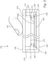
- Fig. 1 schematically illustrates a smartphone 100 comprising an optical biometric imaging device 102 integrated in the display panel of the smartphone 100.
- the optical biometric imaging device 102 is configured to capture an image of an object 104 in contact with an outer surface 106 of the biometric imaging device 102.
- the object 104 in contact with the outer surface 106 is here illustrated as a finger 104 in contact with the surface 106 of the display panel.
- the described device 102 may also be used to capture palmprints.
- Fig. 2 schematically illustrates a biometric imaging device comprising an image sensor 200 which in turn comprises a photodetector pixel array 202 and image sensor circuitry (not shown) configured to capture an image of the object 104 in contact with the outer surface 106 of the imaging device 102.
- the image sensor circuitry may be circuitry integrated in the image sensor 200, external circuitry, or a combination thereof.
- External circuitry for controlling the image sensor 200 may for example include a microprocessor, microcontroller, programmable digital signal processor or another programmable device.
- the image sensor 200 further comprises a first electrically conductive structure 206 arranged adjacent to an active sensing area 208 of the photodetector pixel array 202.
- the photodetector pixel array 202 is arranged on a carrier 204 and the electrically conductive structure 206 is arranged on the carrier 204 adjacent to the photodetector pixel array 202. It is in principle also possible to place the electrically conductive structure 206 on the photodetector pixel array 202, with the caveat that the electrically conductive structure 206 would block light from reaching the pixels directly below the structure 206.
- the optical biometric imaging device 102 further comprises a display panel 210 arranged on top of and at a distance from the image sensor 200, the display panel comprises a second electrically conductive structure 212 on a bottom side 214 of the display panel.
- the bottom side 214 is defined as the side of the display panel 210 facing the image sensor 200.
- the second electrically conductive structure 212 is arranged to face the first electrically conductive structure of the image sensor 206 such that a capacitive coupling between the first and second electrically conductive structures 206, 212 can be detected.
- the light illuminating the finger 104 originates from the display panel 210 arranged above the image sensor 200. Light emitted by light emitting elements of the display panel 210 is reflected by the finger 104 and redirected towards the image sensor 200 in order for the image sensor 200 to capture an image of the finger 104 with sufficient resolution for resolving the fingerprint of the finger 104.
- the optical biometric imaging device may further comprise a frame 216, wherein a cover glass 218 of the display panel 210 is arranged to rest on the frame 216 and wherein the image sensor 200 is arranged within the frame 216.
- the main function of the frame 216 is to carry the display panel 210, and many different configurations of the frame are possible.
- the frame 216 may for example be continuous, semi continuous or consist of individual support structures. It should be noted that the correct distance between the image sensor 200 and the display panel 210 may be achieved in many different ways, also without a frame 216, for example by suitably attaching the display panel 210 and the image sensor 200 to the device 100 in which the biometric imaging device 102 is arranged. It should further be noted that the figures are not drawn to scale, and that the purpose of the figures is to convey principal features of various embodiments of the invention.
- the frame 216 illustrated in Fig. 2 further comprises a floor portion 220. Thereby, a cross section of the frame 216 forms a U-shaped bracket.
- the illustrated frame 216 can thus be seen as a box without a lid, where the image sensor 200 is arranged on the floor 220 of the frame 216.
- the optical biometric imaging device 102 further comprises capacitive readout circuitry (not shown) arranged and configured to detect a capacitance between the first electrically conductive structure 206 and the second electrically conductive structure 212.
- the detected capacitance is proportional to the distance between the first and second electrically conductive structures 206, 212, and a vertical movement of the bottom surface 214 of the display panel 210 can thus be detected by monitoring the capacitance.
- the capacitive readout circuitry may be circuitry integrated in the image sensor 200, external circuitry, or a combination thereof. External circuitry for controlling the capacitive readout may for example include a microprocessor, microcontroller, programmable digital signal processor or another programmable device.
- the first and second electrically conductive structures 206, 212 face each other to form a parallel plate capacitor with an air gap as the dielectric layer.
- the first and second electrically conductive structures 206, 212 may for example be formed by depositing a respective metal layer. Moreover, it is not required that the two electrically conductive structures 206, 212 are of the same size. It is also possible to provide a plurality of electrically conductive structures 206, 212 on the display panel 210 and on the image sensor respectively, to form a plurality of capacitors, in order to detect a vertical movement of the display panel 210 in relation to the image sensor 200 at multiple locations.
- Fig. 3 illustrates an example embodiment of the optical biometric imaging device 102 further comprising a spacer 300 arranged on the carrier 204 adjacent to the first electrically conductive structure 206.
- the spacer 300 may have height which is larger than the thickness of the image sensor 200 in order to act as mechanical protection for the image sensor 200, thereby preventing that the display panel 210 makes contact with the photodetector pixel array 202.
- Fig. 4 illustrates an example embodiment of the optical biometric imaging device where a spacer 300 is arranged between the carrier 204 and the first electrically conductive structure 206.
- the first electrically conductive structure 206 is arranged on top of the spacer 300.
- Fig. 5 illustrates an example embodiment of the optical biometric imaging device 102 where the floor portion 220 of the frame 216 comprises a recess 500, and wherein the image sensor 200 is arranged in the recess 500 of the floor portion 220.
- Fig. 6 illustrates an example embodiment of the optical biometric imaging device 102 where the floor portion 220 comprises a through-opening 600, and wherein the image sensor 200 is arranged in the through-opening 600 of the floor portion 220.
- the frame 216 and the image sensor 200 may thus be arranged on another structural element, which for example may be a part of a deice in which the optical biometric imaging device 102 is arranged.
- Fig. 7 illustrates an example embodiment of the optical biometric imaging device 102 where the floor portion 220 comprises a through-opening 600, and wherein the image sensor 200 is arranged below the through-opening 600 of the floor portion 220.
- spacers 300 may be used to attach the image sensor 200 to a bottom side of the frame 216.
- the spacers 300 may for example be attached to the frame 216 by means of an adhesive.
- Fig. 8 schematically illustrates the optical biometric imaging device 102 when a finger 104 is pressing down on the outer surface 106 of the device, e.g. the cover glass 218 of the display panel 210.
- a display panel such as an AMOLED panel has a certain flexibility, and when a finger 104 is pressing on the panel with sufficient force, the flexible display panel 210 will deform and bend down in response to and proportional with the applied force.
- the reduced distance between the first and second electrically conductive structure 206, 212 produces a corresponding increase in capacitance C, which is proportional to the applied force F. Since the demagnification factor ( Demag ) is proportional to the distance between the object and the image sensor, Demag is inversely proportional to the force F. the relations can be described as:
- Fig. 9 schematically illustrates a biometric imaging device according to an embodiment of the invention where the optical properties of the device are illustrated.
- H o illustrates the object distance
- H i is the image distance
- a o is object area
- a i is the image area.
- the demagnification factor is calculated by the ratio of H o and H i .
- H i is fixed within the imaging device 102, while the distance H o is subject to change depending on a force applied to the top of the cover glass 218.
- d changes when H o changes, so the Demag depends on the changed H o which can be determined based on the change in d.
- the relation between a change in d and a change in H0 is known for a given device so that a change in H0 can be derived based on a change of capacitance between the first electrically conductive structure 206 a second electrically conductive structure 212.
- Fig. 9 further illustrates that the second electrically conductive structure 212 is larger than the first electrically conductive structure 206.
Landscapes
- Engineering & Computer Science (AREA)
- Theoretical Computer Science (AREA)
- General Engineering & Computer Science (AREA)
- Physics & Mathematics (AREA)
- General Physics & Mathematics (AREA)
- Human Computer Interaction (AREA)
- Computer Hardware Design (AREA)
- Computer Security & Cryptography (AREA)
- Software Systems (AREA)
- Image Input (AREA)
- Measurement Of The Respiration, Hearing Ability, Form, And Blood Characteristics Of Living Organisms (AREA)
- Multimedia (AREA)
Claims (14)
- Dispositif d'imagerie biométrique optique (102) configuré pour capturer une image d'un objet (104) en contact avec une surface extérieure (106) du dispositif d'imagerie biométrique, le dispositif d'imagerie biométrique comprenant :un capteur d'image (200) comprenant un réseau de pixels photodétecteurs (202) et une circuiterie de capteur d'image configurée pour capturer une image de l'objet en contact avec la surface extérieure du dispositif d'imagerie ;le capteur d'image comprenant une première structure électriquement conductrice (206) agencée adjacente à une zone de détection active (208) du réseau de pixels photodétecteurs ;un panneau d'affichage (210) agencé au-dessus et à distance du capteur d'image, le panneau d'affichage comprenant une deuxième structure électriquement conductrice (212) sur un côté inférieur (214) du panneau d'affichage et agencée pour faire face à la première structure électriquement conductrice du capteur d'image ; etune circuiterie de lecture capacitive agencée et configurée pour détecter une capacité entre la première structure électriquement conductrice et la deuxième structure électriquement conductrice, dans lequel le capteur d'image est configurée pour déterminer un facteur de dégrossissement du dispositif d'imagerie biométrique sur la base d'une relation connue entre la capacité détectée et la distance entre les première et deuxième structures électriquement conductrices.
- Dispositif d'imagerie biométrique optique selon la revendication 1, comprenant en outre un cadre (216), dans lequel un verre de couverture (218) du panneau d'affichage est agencé pour reposer sur le cadre et le capteur d'image est agencé à l'intérieur du cadre.
- Dispositif d'imagerie biométrique optique selon la revendication 1 ou 2, comprenant en outre un porteur (204), dans lequel le réseau de pixels photodétecteurs est agencé sur le porteur et la première structure électriquement conductrice est agencée sur le porteur adjacente au réseau de pixels photodétecteurs.
- Dispositif d'imagerie biométrique optique selon la revendication 3, comprenant en outre une entretoise (300) agencée sur le porteur adjacente à la première structure électriquement conductrice.
- Dispositif d'imagerie biométrique optique selon la revendication 3, comprenant en outre une entretoise (300) agencée entre le porteur et la première structure électriquement conductrice.
- Dispositif d'imagerie biométrique optique selon l'une quelconque des revendications précédentes, comprenant une pluralité desdites premières structures électriquement conductrices.
- Dispositif d'imagerie biométrique optique selon la revendication 6, dans lequel le panneau d'affichage comprend une pluralité desdites deuxièmes structures électriquement conductrices.
- Dispositif d'imagerie biométrique optique selon la revendication 2, dans lequel le cadre comprend une partie de plancher (220), formant ainsi une coupe transversale de support en forme de U.
- Dispositif d'imagerie biométrique optique selon la revendication 8, dans lequel le capteur d'image est agencé sur la partie de plancher du support.
- Dispositif d'imagerie biométrique optique selon la revendication 8, dans lequel la partie de plancher comprend un évidement (500), dans lequel le capteur d'image est agencé dans l'évidement de la partie de plancher.
- Dispositif d'imagerie biométrique optique selon la revendication 8, dans lequel la partie de plancher comprend une ouverture traversante (600), dans lequel le capteur d'image est agencé dans l'ouverture traversante de la partie de plancher.
- Dispositif d'imagerie biométrique optique selon la revendication 8, dans lequel la partie de plancher comprend une ouverture traversante (600), dans lequel le capteur d'image est agencé au-dessous de l'ouverture traversante de la partie de plancher.
- Procédé de détection d'une force sur une surface d'un dispositif d'imagerie biométrique optique (102) configuré pour capturer une image d'un objet (104) en contact avec une surface extérieure (106) du dispositif d'imagerie biométrique, le dispositif d'imagerie biométrique comprenant :un capteur d'image (200) comprenant un réseau de pixels photodétecteurs (202) et une circuiterie de capteur d'image (210) configurée pour capturer une image d'un objet en contact avec une surface extérieure du dispositif d'imagerie ;le capteur d'image comprenant une première structure électriquement conductrice agencée sur une surface supérieure du capteur d'image et adjacente à une zone de détection active du réseau de pixels photodétecteurs ;un panneau d'affichage agencé au-dessus et à distance du capteur d'image ;le panneau d'affichage comprenant une deuxième structure électriquement conductrice sur un côté inférieur du panneau d'affichage agencée pour faire face à la première structure électriquement conductrice du capteur d'image ; etune circuiterie de lecture capacitive agencée et configurée pour détecter une capacité entre la première structure électriquement conductrice et la deuxième structure électriquement conductrice ;le procédé comprenant la détection d'un changement de capacité entre les première et deuxième structures électriquement conductrices et la détermination d'un facteur de dégrossissement du dispositif d'imagerie biométrique sur la base d'une relation connue entre la capacité et la distance entre les première et deuxième structures électriquement conductrices.
- Procédé selon la revendication 13, comprenant en outre la détermination d'une force sur la surface extérieure du dispositif d'imagerie biométrique sur la base d'une relation connue entre la capacité et la distance entre les première et deuxième structures électriquement conductrices.
Applications Claiming Priority (1)
| Application Number | Priority Date | Filing Date | Title |
|---|---|---|---|
| PCT/CN2018/104161 WO2020047770A1 (fr) | 2018-09-05 | 2018-09-05 | Module de capteur d'empreinte digitale optique et procédé de fonctionnement d'un module de d'empreinte digitale optique |
Publications (3)
| Publication Number | Publication Date |
|---|---|
| EP3847533A1 EP3847533A1 (fr) | 2021-07-14 |
| EP3847533A4 EP3847533A4 (fr) | 2021-09-22 |
| EP3847533B1 true EP3847533B1 (fr) | 2024-11-13 |
Family
ID=69722712
Family Applications (1)
| Application Number | Title | Priority Date | Filing Date |
|---|---|---|---|
| EP18932346.2A Active EP3847533B1 (fr) | 2018-09-05 | 2018-09-05 | Module de capteur d'empreinte digitale optique et procédé de fonctionnement d'un module de d'empreinte digitale optique |
Country Status (4)
| Country | Link |
|---|---|
| US (1) | US11398104B2 (fr) |
| EP (1) | EP3847533B1 (fr) |
| CN (1) | CN112639705B (fr) |
| WO (1) | WO2020047770A1 (fr) |
Citations (2)
| Publication number | Priority date | Publication date | Assignee | Title |
|---|---|---|---|---|
| US20160033342A1 (en) * | 2013-03-15 | 2016-02-04 | Apple Inc. | Force-Sensitive Fingerprint Sensing Input |
| WO2018155851A1 (fr) * | 2017-02-24 | 2018-08-30 | 삼성전자 주식회사 | Dispositif électronique comprenant un biocapteur intégré dans un dispositif d'affichage |
Family Cites Families (24)
| Publication number | Priority date | Publication date | Assignee | Title |
|---|---|---|---|---|
| AU4330100A (en) | 1999-04-05 | 2000-10-23 | Ethentica, Inc. | Planar optical image sensor and system for generating an electronic image of a relief object for fingerprint reading |
| AU2001255172A1 (en) * | 2000-03-10 | 2001-09-24 | Ethentica, Inc. | Biometric sensor |
| JP4658443B2 (ja) | 2002-12-19 | 2011-03-23 | カシオ計算機株式会社 | 画像入力装置 |
| US7148882B2 (en) * | 2003-05-16 | 2006-12-12 | 3M Innovatie Properties Company | Capacitor based force sensor |
| JP2005004718A (ja) | 2003-05-16 | 2005-01-06 | Canon Inc | 信号処理装置及び制御方法 |
| US8463001B2 (en) * | 2007-07-30 | 2013-06-11 | Sony Corporation | Image pickup apparatus |
| WO2009020940A2 (fr) * | 2007-08-03 | 2009-02-12 | Perceptive Pixel, Inc. | Détection tactile multipoint par le biais d'une réflexion interne totale frustrée |
| WO2011070660A1 (fr) | 2009-12-09 | 2011-06-16 | 富士通株式会社 | Détecteur de capacité et procédé de formation d'une image biologique |
| US8724038B2 (en) | 2010-10-18 | 2014-05-13 | Qualcomm Mems Technologies, Inc. | Wraparound assembly for combination touch, handwriting and fingerprint sensor |
| US9836165B2 (en) | 2014-05-16 | 2017-12-05 | Apple Inc. | Integrated silicon-OLED display and touch sensor panel |
| WO2016055007A1 (fr) | 2014-10-06 | 2016-04-14 | Shenzhen Huiding Technology Co., Ltd. | Capteur d'empreinte digitale à capacité répartie avec des pixels amplifiés actifs |
| US10732771B2 (en) | 2014-11-12 | 2020-08-04 | Shenzhen GOODIX Technology Co., Ltd. | Fingerprint sensors having in-pixel optical sensors |
| US10437974B2 (en) | 2015-06-18 | 2019-10-08 | Shenzhen GOODIX Technology Co., Ltd. | Optical sensing performance of under-screen optical sensor module for on-screen fingerprint sensing |
| DE102015110496B4 (de) * | 2015-06-30 | 2018-06-14 | Infineon Technologies Dresden Gmbh | Integriertes, lichtemittierendes bauelement,integriertes sensorbauelement undherstellungsverfahren |
| US20180326456A1 (en) | 2015-11-06 | 2018-11-15 | Moda-Innochips Co., Ltd. | Pressure sensor, and composite element and electronic device having same |
| US10268884B2 (en) | 2016-01-29 | 2019-04-23 | Synaptics Incorporated | Optical fingerprint sensor under a display |
| WO2017183910A2 (fr) | 2016-04-19 | 2017-10-26 | Samsung Electronics Co., Ltd. | Dispositif électronique permettant la vérification d'empreinte digitale et son procédé de fonctionnement |
| JP6684167B2 (ja) * | 2016-06-27 | 2020-04-22 | 株式会社ジャパンディスプレイ | 表示装置 |
| EP3485342B1 (fr) | 2016-07-18 | 2021-02-17 | Shenzhen Goodix Technology Co., Ltd. | Capteur optique d'empreintes digitales avec capacité de détection de force |
| KR102589636B1 (ko) | 2016-08-05 | 2023-10-17 | 삼성전자주식회사 | 지문 센서를 포함하는 전자 장치 |
| US10102411B2 (en) | 2017-01-25 | 2018-10-16 | Synaptics Incorporated | Hybrid optical and capacitive sensor |
| KR101910518B1 (ko) * | 2017-04-11 | 2018-10-22 | 삼성전자주식회사 | 생체 센서 및 생체 센서를 포함하는 장치 |
| KR102364678B1 (ko) * | 2017-06-20 | 2022-02-18 | 엘지전자 주식회사 | 이동 단말기 |
| KR102447185B1 (ko) * | 2018-01-02 | 2022-09-27 | 삼성전자 주식회사 | 포스 센서의 압력값 보상 방법 및 이를 사용하는 전자 장치 |
-
2018
- 2018-09-05 EP EP18932346.2A patent/EP3847533B1/fr active Active
- 2018-09-05 WO PCT/CN2018/104161 patent/WO2020047770A1/fr not_active Ceased
- 2018-09-05 CN CN201880096933.1A patent/CN112639705B/zh active Active
- 2018-09-05 US US17/272,577 patent/US11398104B2/en active Active
Patent Citations (3)
| Publication number | Priority date | Publication date | Assignee | Title |
|---|---|---|---|---|
| US20160033342A1 (en) * | 2013-03-15 | 2016-02-04 | Apple Inc. | Force-Sensitive Fingerprint Sensing Input |
| WO2018155851A1 (fr) * | 2017-02-24 | 2018-08-30 | 삼성전자 주식회사 | Dispositif électronique comprenant un biocapteur intégré dans un dispositif d'affichage |
| US20200057467A1 (en) * | 2017-02-24 | 2020-02-20 | Samsung Electronics Co., Ltd. | Electronic device comprising biometric sensor integrated in display |
Also Published As
| Publication number | Publication date |
|---|---|
| US20210312157A1 (en) | 2021-10-07 |
| EP3847533A4 (fr) | 2021-09-22 |
| CN112639705B (zh) | 2023-08-01 |
| EP3847533A1 (fr) | 2021-07-14 |
| WO2020047770A1 (fr) | 2020-03-12 |
| CN112639705A (zh) | 2021-04-09 |
| US11398104B2 (en) | 2022-07-26 |
Similar Documents
| Publication | Publication Date | Title |
|---|---|---|
| NL2019962B1 (en) | Capacitive sensor packaging | |
| AU2016100377B4 (en) | Biometric sensor stack structure | |
| AU2013100571A4 (en) | Capacitive sensor packaging | |
| EP3847533B1 (fr) | Module de capteur d'empreinte digitale optique et procédé de fonctionnement d'un module de d'empreinte digitale optique | |
| AU2013101650B4 (en) | Capacitive sensor packaging | |
| HK1208901B (en) | Capacitive sensor packaging |
Legal Events
| Date | Code | Title | Description |
|---|---|---|---|
| STAA | Information on the status of an ep patent application or granted ep patent |
Free format text: STATUS: THE INTERNATIONAL PUBLICATION HAS BEEN MADE |
|
| PUAI | Public reference made under article 153(3) epc to a published international application that has entered the european phase |
Free format text: ORIGINAL CODE: 0009012 |
|
| STAA | Information on the status of an ep patent application or granted ep patent |
Free format text: STATUS: REQUEST FOR EXAMINATION WAS MADE |
|
| 17P | Request for examination filed |
Effective date: 20210205 |
|
| AK | Designated contracting states |
Kind code of ref document: A1 Designated state(s): AL AT BE BG CH CY CZ DE DK EE ES FI FR GB GR HR HU IE IS IT LI LT LU LV MC MK MT NL NO PL PT RO RS SE SI SK SM TR |
|
| A4 | Supplementary search report drawn up and despatched |
Effective date: 20210819 |
|
| RIC1 | Information provided on ipc code assigned before grant |
Ipc: G06F 21/32 20130101ALI20210813BHEP Ipc: G06F 3/044 20060101AFI20210813BHEP |
|
| RAP1 | Party data changed (applicant data changed or rights of an application transferred) |
Owner name: FINGERPRINT CARDS ANACATUM IP AB |
|
| DAV | Request for validation of the european patent (deleted) | ||
| DAX | Request for extension of the european patent (deleted) | ||
| STAA | Information on the status of an ep patent application or granted ep patent |
Free format text: STATUS: EXAMINATION IS IN PROGRESS |
|
| 17Q | First examination report despatched |
Effective date: 20231002 |
|
| REG | Reference to a national code |
Free format text: PREVIOUS MAIN CLASS: G06F0003044000 Ipc: G06F0001160000 Ref country code: DE Ref legal event code: R079 Ref document number: 602018076634 Country of ref document: DE Free format text: PREVIOUS MAIN CLASS: G06F0003044000 Ipc: G06F0001160000 |
|
| GRAP | Despatch of communication of intention to grant a patent |
Free format text: ORIGINAL CODE: EPIDOSNIGR1 |
|
| STAA | Information on the status of an ep patent application or granted ep patent |
Free format text: STATUS: GRANT OF PATENT IS INTENDED |
|
| RIC1 | Information provided on ipc code assigned before grant |
Ipc: G06F 21/32 20130101ALI20240501BHEP Ipc: G06F 3/044 20060101ALI20240501BHEP Ipc: G06F 1/16 20060101AFI20240501BHEP |
|
| INTG | Intention to grant announced |
Effective date: 20240517 |
|
| GRAS | Grant fee paid |
Free format text: ORIGINAL CODE: EPIDOSNIGR3 |
|
| GRAA | (expected) grant |
Free format text: ORIGINAL CODE: 0009210 |
|
| STAA | Information on the status of an ep patent application or granted ep patent |
Free format text: STATUS: THE PATENT HAS BEEN GRANTED |
|
| AK | Designated contracting states |
Kind code of ref document: B1 Designated state(s): AL AT BE BG CH CY CZ DE DK EE ES FI FR GB GR HR HU IE IS IT LI LT LU LV MC MK MT NL NO PL PT RO RS SE SI SK SM TR |
|
| REG | Reference to a national code |
Ref country code: GB Ref legal event code: FG4D |
|
| REG | Reference to a national code |
Ref country code: CH Ref legal event code: EP |
|
| REG | Reference to a national code |
Ref country code: IE Ref legal event code: FG4D |
|
| REG | Reference to a national code |
Ref country code: DE Ref legal event code: R096 Ref document number: 602018076634 Country of ref document: DE |
|
| REG | Reference to a national code |
Ref country code: LT Ref legal event code: MG9D |
|
| REG | Reference to a national code |
Ref country code: NL Ref legal event code: MP Effective date: 20241113 |
|
| PG25 | Lapsed in a contracting state [announced via postgrant information from national office to epo] |
Ref country code: IS Free format text: LAPSE BECAUSE OF FAILURE TO SUBMIT A TRANSLATION OF THE DESCRIPTION OR TO PAY THE FEE WITHIN THE PRESCRIBED TIME-LIMIT Effective date: 20250313 Ref country code: PT Free format text: LAPSE BECAUSE OF FAILURE TO SUBMIT A TRANSLATION OF THE DESCRIPTION OR TO PAY THE FEE WITHIN THE PRESCRIBED TIME-LIMIT Effective date: 20250313 Ref country code: HR Free format text: LAPSE BECAUSE OF FAILURE TO SUBMIT A TRANSLATION OF THE DESCRIPTION OR TO PAY THE FEE WITHIN THE PRESCRIBED TIME-LIMIT Effective date: 20241113 |
|
| PG25 | Lapsed in a contracting state [announced via postgrant information from national office to epo] |
Ref country code: FI Free format text: LAPSE BECAUSE OF FAILURE TO SUBMIT A TRANSLATION OF THE DESCRIPTION OR TO PAY THE FEE WITHIN THE PRESCRIBED TIME-LIMIT Effective date: 20241113 Ref country code: NL Free format text: LAPSE BECAUSE OF FAILURE TO SUBMIT A TRANSLATION OF THE DESCRIPTION OR TO PAY THE FEE WITHIN THE PRESCRIBED TIME-LIMIT Effective date: 20241113 |
|
| REG | Reference to a national code |
Ref country code: AT Ref legal event code: MK05 Ref document number: 1742162 Country of ref document: AT Kind code of ref document: T Effective date: 20241113 |
|
| PG25 | Lapsed in a contracting state [announced via postgrant information from national office to epo] |
Ref country code: BG Free format text: LAPSE BECAUSE OF FAILURE TO SUBMIT A TRANSLATION OF THE DESCRIPTION OR TO PAY THE FEE WITHIN THE PRESCRIBED TIME-LIMIT Effective date: 20241113 |
|
| PG25 | Lapsed in a contracting state [announced via postgrant information from national office to epo] |
Ref country code: ES Free format text: LAPSE BECAUSE OF FAILURE TO SUBMIT A TRANSLATION OF THE DESCRIPTION OR TO PAY THE FEE WITHIN THE PRESCRIBED TIME-LIMIT Effective date: 20241113 |
|
| PG25 | Lapsed in a contracting state [announced via postgrant information from national office to epo] |
Ref country code: NO Free format text: LAPSE BECAUSE OF FAILURE TO SUBMIT A TRANSLATION OF THE DESCRIPTION OR TO PAY THE FEE WITHIN THE PRESCRIBED TIME-LIMIT Effective date: 20250213 |
|
| PG25 | Lapsed in a contracting state [announced via postgrant information from national office to epo] |
Ref country code: AT Free format text: LAPSE BECAUSE OF FAILURE TO SUBMIT A TRANSLATION OF THE DESCRIPTION OR TO PAY THE FEE WITHIN THE PRESCRIBED TIME-LIMIT Effective date: 20241113 Ref country code: LV Free format text: LAPSE BECAUSE OF FAILURE TO SUBMIT A TRANSLATION OF THE DESCRIPTION OR TO PAY THE FEE WITHIN THE PRESCRIBED TIME-LIMIT Effective date: 20241113 Ref country code: GR Free format text: LAPSE BECAUSE OF FAILURE TO SUBMIT A TRANSLATION OF THE DESCRIPTION OR TO PAY THE FEE WITHIN THE PRESCRIBED TIME-LIMIT Effective date: 20250214 |
|
| PG25 | Lapsed in a contracting state [announced via postgrant information from national office to epo] |
Ref country code: PL Free format text: LAPSE BECAUSE OF FAILURE TO SUBMIT A TRANSLATION OF THE DESCRIPTION OR TO PAY THE FEE WITHIN THE PRESCRIBED TIME-LIMIT Effective date: 20241113 |
|
| PG25 | Lapsed in a contracting state [announced via postgrant information from national office to epo] |
Ref country code: RS Free format text: LAPSE BECAUSE OF FAILURE TO SUBMIT A TRANSLATION OF THE DESCRIPTION OR TO PAY THE FEE WITHIN THE PRESCRIBED TIME-LIMIT Effective date: 20250213 |
|
| PG25 | Lapsed in a contracting state [announced via postgrant information from national office to epo] |
Ref country code: SM Free format text: LAPSE BECAUSE OF FAILURE TO SUBMIT A TRANSLATION OF THE DESCRIPTION OR TO PAY THE FEE WITHIN THE PRESCRIBED TIME-LIMIT Effective date: 20241113 |
|
| PG25 | Lapsed in a contracting state [announced via postgrant information from national office to epo] |
Ref country code: DK Free format text: LAPSE BECAUSE OF FAILURE TO SUBMIT A TRANSLATION OF THE DESCRIPTION OR TO PAY THE FEE WITHIN THE PRESCRIBED TIME-LIMIT Effective date: 20241113 |
|
| PG25 | Lapsed in a contracting state [announced via postgrant information from national office to epo] |
Ref country code: EE Free format text: LAPSE BECAUSE OF FAILURE TO SUBMIT A TRANSLATION OF THE DESCRIPTION OR TO PAY THE FEE WITHIN THE PRESCRIBED TIME-LIMIT Effective date: 20241113 |
|
| PG25 | Lapsed in a contracting state [announced via postgrant information from national office to epo] |
Ref country code: RO Free format text: LAPSE BECAUSE OF FAILURE TO SUBMIT A TRANSLATION OF THE DESCRIPTION OR TO PAY THE FEE WITHIN THE PRESCRIBED TIME-LIMIT Effective date: 20241113 |
|
| PG25 | Lapsed in a contracting state [announced via postgrant information from national office to epo] |
Ref country code: SK Free format text: LAPSE BECAUSE OF FAILURE TO SUBMIT A TRANSLATION OF THE DESCRIPTION OR TO PAY THE FEE WITHIN THE PRESCRIBED TIME-LIMIT Effective date: 20241113 |
|
| PG25 | Lapsed in a contracting state [announced via postgrant information from national office to epo] |
Ref country code: CZ Free format text: LAPSE BECAUSE OF FAILURE TO SUBMIT A TRANSLATION OF THE DESCRIPTION OR TO PAY THE FEE WITHIN THE PRESCRIBED TIME-LIMIT Effective date: 20241113 |
|
| PG25 | Lapsed in a contracting state [announced via postgrant information from national office to epo] |
Ref country code: IT Free format text: LAPSE BECAUSE OF FAILURE TO SUBMIT A TRANSLATION OF THE DESCRIPTION OR TO PAY THE FEE WITHIN THE PRESCRIBED TIME-LIMIT Effective date: 20241113 |
|
| REG | Reference to a national code |
Ref country code: DE Ref legal event code: R097 Ref document number: 602018076634 Country of ref document: DE |
|
| PG25 | Lapsed in a contracting state [announced via postgrant information from national office to epo] |
Ref country code: SE Free format text: LAPSE BECAUSE OF FAILURE TO SUBMIT A TRANSLATION OF THE DESCRIPTION OR TO PAY THE FEE WITHIN THE PRESCRIBED TIME-LIMIT Effective date: 20241113 |
|
| PLBE | No opposition filed within time limit |
Free format text: ORIGINAL CODE: 0009261 |
|
| STAA | Information on the status of an ep patent application or granted ep patent |
Free format text: STATUS: NO OPPOSITION FILED WITHIN TIME LIMIT |
|
| 26N | No opposition filed |
Effective date: 20250814 |
|
| REG | Reference to a national code |
Ref country code: CH Ref legal event code: H13 Free format text: ST27 STATUS EVENT CODE: U-0-0-H10-H13 (AS PROVIDED BY THE NATIONAL OFFICE) Effective date: 20260425 |