EP3848965A1 - Bilderzeugendes festkörperelement, bilderzeugendes system, verfahren zum betrieb des bilderzeugenden festkörperelements, und fotodetektor - Google Patents
Bilderzeugendes festkörperelement, bilderzeugendes system, verfahren zum betrieb des bilderzeugenden festkörperelements, und fotodetektor Download PDFInfo
- Publication number
- EP3848965A1 EP3848965A1 EP19857977.3A EP19857977A EP3848965A1 EP 3848965 A1 EP3848965 A1 EP 3848965A1 EP 19857977 A EP19857977 A EP 19857977A EP 3848965 A1 EP3848965 A1 EP 3848965A1
- Authority
- EP
- European Patent Office
- Prior art keywords
- pixel
- readout
- photon
- solid
- image sensor
- Prior art date
- Legal status (The legal status is an assumption and is not a legal conclusion. Google has not performed a legal analysis and makes no representation as to the accuracy of the status listed.)
- Withdrawn
Links
Images




Classifications
-
- H—ELECTRICITY
- H10—SEMICONDUCTOR DEVICES; ELECTRIC SOLID-STATE DEVICES NOT OTHERWISE PROVIDED FOR
- H10F—INORGANIC SEMICONDUCTOR DEVICES SENSITIVE TO INFRARED RADIATION, LIGHT, ELECTROMAGNETIC RADIATION OF SHORTER WAVELENGTH OR CORPUSCULAR RADIATION
- H10F39/00—Integrated devices, or assemblies of multiple devices, comprising at least one element covered by group H10F30/00, e.g. radiation detectors comprising photodiode arrays
- H10F39/80—Constructional details of image sensors
- H10F39/806—Optical elements or arrangements associated with the image sensors
-
- H—ELECTRICITY
- H04—ELECTRIC COMMUNICATION TECHNIQUE
- H04N—PICTORIAL COMMUNICATION, e.g. TELEVISION
- H04N25/00—Circuitry of solid-state image sensors [SSIS]; Control thereof
- H04N25/50—Control of the SSIS exposure
-
- G—PHYSICS
- G01—MEASURING; TESTING
- G01S—RADIO DIRECTION-FINDING; RADIO NAVIGATION; DETERMINING DISTANCE OR VELOCITY BY USE OF RADIO WAVES; LOCATING OR PRESENCE-DETECTING BY USE OF THE REFLECTION OR RERADIATION OF RADIO WAVES; ANALOGOUS ARRANGEMENTS USING OTHER WAVES
- G01S17/00—Systems using the reflection or reradiation of electromagnetic waves other than radio waves, e.g. lidar systems
- G01S17/02—Systems using the reflection of electromagnetic waves other than radio waves
- G01S17/06—Systems determining position data of a target
- G01S17/08—Systems determining position data of a target for measuring distance only
- G01S17/10—Systems determining position data of a target for measuring distance only using transmission of interrupted, pulse-modulated waves
- G01S17/18—Systems determining position data of a target for measuring distance only using transmission of interrupted, pulse-modulated waves wherein range gates are used
-
- G—PHYSICS
- G01—MEASURING; TESTING
- G01S—RADIO DIRECTION-FINDING; RADIO NAVIGATION; DETERMINING DISTANCE OR VELOCITY BY USE OF RADIO WAVES; LOCATING OR PRESENCE-DETECTING BY USE OF THE REFLECTION OR RERADIATION OF RADIO WAVES; ANALOGOUS ARRANGEMENTS USING OTHER WAVES
- G01S17/00—Systems using the reflection or reradiation of electromagnetic waves other than radio waves, e.g. lidar systems
- G01S17/88—Lidar systems specially adapted for specific applications
- G01S17/89—Lidar systems specially adapted for specific applications for mapping or imaging
-
- H—ELECTRICITY
- H04—ELECTRIC COMMUNICATION TECHNIQUE
- H04N—PICTORIAL COMMUNICATION, e.g. TELEVISION
- H04N25/00—Circuitry of solid-state image sensors [SSIS]; Control thereof
-
- H—ELECTRICITY
- H04—ELECTRIC COMMUNICATION TECHNIQUE
- H04N—PICTORIAL COMMUNICATION, e.g. TELEVISION
- H04N25/00—Circuitry of solid-state image sensors [SSIS]; Control thereof
- H04N25/70—SSIS architectures; Circuits associated therewith
- H04N25/703—SSIS architectures incorporating pixels for producing signals other than image signals
- H04N25/707—Pixels for event detection
-
- H—ELECTRICITY
- H04—ELECTRIC COMMUNICATION TECHNIQUE
- H04N—PICTORIAL COMMUNICATION, e.g. TELEVISION
- H04N25/00—Circuitry of solid-state image sensors [SSIS]; Control thereof
- H04N25/70—SSIS architectures; Circuits associated therewith
- H04N25/76—Addressed sensors, e.g. MOS or CMOS sensors
- H04N25/77—Pixel circuitry, e.g. memories, A/D converters, pixel amplifiers, shared circuits or shared components
-
- H—ELECTRICITY
- H04—ELECTRIC COMMUNICATION TECHNIQUE
- H04N—PICTORIAL COMMUNICATION, e.g. TELEVISION
- H04N25/00—Circuitry of solid-state image sensors [SSIS]; Control thereof
- H04N25/70—SSIS architectures; Circuits associated therewith
- H04N25/76—Addressed sensors, e.g. MOS or CMOS sensors
- H04N25/77—Pixel circuitry, e.g. memories, A/D converters, pixel amplifiers, shared circuits or shared components
- H04N25/772—Pixel circuitry, e.g. memories, A/D converters, pixel amplifiers, shared circuits or shared components comprising A/D, V/T, V/F, I/T or I/F converters
- H04N25/773—Pixel circuitry, e.g. memories, A/D converters, pixel amplifiers, shared circuits or shared components comprising A/D, V/T, V/F, I/T or I/F converters comprising photon counting circuits, e.g. single photon detection [SPD] or single photon avalanche diodes [SPAD]
-
- H—ELECTRICITY
- H04—ELECTRIC COMMUNICATION TECHNIQUE
- H04N—PICTORIAL COMMUNICATION, e.g. TELEVISION
- H04N25/00—Circuitry of solid-state image sensors [SSIS]; Control thereof
- H04N25/70—SSIS architectures; Circuits associated therewith
- H04N25/76—Addressed sensors, e.g. MOS or CMOS sensors
- H04N25/78—Readout circuits for addressed sensors, e.g. output amplifiers or A/D converters
-
- H—ELECTRICITY
- H10—SEMICONDUCTOR DEVICES; ELECTRIC SOLID-STATE DEVICES NOT OTHERWISE PROVIDED FOR
- H10F—INORGANIC SEMICONDUCTOR DEVICES SENSITIVE TO INFRARED RADIATION, LIGHT, ELECTROMAGNETIC RADIATION OF SHORTER WAVELENGTH OR CORPUSCULAR RADIATION
- H10F39/00—Integrated devices, or assemblies of multiple devices, comprising at least one element covered by group H10F30/00, e.g. radiation detectors comprising photodiode arrays
- H10F39/10—Integrated devices
- H10F39/12—Image sensors
- H10F39/18—Complementary metal-oxide-semiconductor [CMOS] image sensors; Photodiode array image sensors
-
- H—ELECTRICITY
- H10—SEMICONDUCTOR DEVICES; ELECTRIC SOLID-STATE DEVICES NOT OTHERWISE PROVIDED FOR
- H10F—INORGANIC SEMICONDUCTOR DEVICES SENSITIVE TO INFRARED RADIATION, LIGHT, ELECTROMAGNETIC RADIATION OF SHORTER WAVELENGTH OR CORPUSCULAR RADIATION
- H10F39/00—Integrated devices, or assemblies of multiple devices, comprising at least one element covered by group H10F30/00, e.g. radiation detectors comprising photodiode arrays
- H10F39/80—Constructional details of image sensors
- H10F39/803—Pixels having integrated switching, control, storage or amplification elements
-
- G—PHYSICS
- G01—MEASURING; TESTING
- G01S—RADIO DIRECTION-FINDING; RADIO NAVIGATION; DETERMINING DISTANCE OR VELOCITY BY USE OF RADIO WAVES; LOCATING OR PRESENCE-DETECTING BY USE OF THE REFLECTION OR RERADIATION OF RADIO WAVES; ANALOGOUS ARRANGEMENTS USING OTHER WAVES
- G01S7/00—Details of systems according to groups G01S13/00, G01S15/00, G01S17/00
- G01S7/48—Details of systems according to groups G01S13/00, G01S15/00, G01S17/00 of systems according to group G01S17/00
- G01S7/483—Details of pulse systems
- G01S7/486—Receivers
- G01S7/4861—Circuits for detection, sampling, integration or read-out
- G01S7/4863—Detector arrays, e.g. charge-transfer gates
Definitions
- the present disclosure relates to a solid-state image sensor, and particularly to a solid-state image sensor including a device in which avalanche multiplication occurs with one photon.
- Patent Documents 1 and 2 describe examples of such a solid-state image sensor.
- an APD arranged in each of the pixel cells multiply charges generated by photoelectric conversion, and a determination circuit disposed in the pixel cell determine whether photons are detected or not so that a result of this determination is stored or added in a memory in the pixel cell.
- a series of such operations that is, detection, determination, and addition, is repeated multiple times.
- Information accumulated in the memories of the pixel cells are output as an image of one frame.
- each pixel cell has a relatively large circuit scale, and thus, it is difficult to miniaturize the pixel cells.
- the pixel cell needs to wait for entry of a plurality of photons, the time necessary for readout of an image is relatively long.
- an AD converter is needed in order to digitize a voltage corresponding to the number of photons which have entered.
- a solid-state image sensor includes: a pixel array including a plurality of pixel cells; a pixel driving circuit configured to drive the plurality of pixel cells; a readout circuit configured to read data from the plurality of pixel cells and output an image constituted by pixels corresponding to the plurality of pixel cells; and a plurality of readout wires corresponding to respective columns of the pixel cells, the plurality of readout wires connecting the pixel cell and the readout circuit to each other.
- Each of the plurality of pixel cells includes an avalanche photodiode configured to detect a photon by avalanche multiplication occurring when one photon enters, and a transfer transistor configured to transfer a detection result of the photon by the avalanche photodiode to a corresponding one of the readout wires.
- the readout circuit determines whether a photon is detected or not based on a voltage of one of the readout wires corresponding to the pixel cell, and outputs a determination result as a value of a pixel corresponding to the pixel cell.
- This configuration eliminates the necessity for determination on whether a photon is detected or not and holding of a determination result in pixel cells.
- the pixel cells can be made in a small circuit scale and further miniaturized. Since the solid-state image sensor according to the present disclosure does not need to wait for entry of a plurality of photons, the time necessary for readout of an image can be further reduced. Data on whether a photon is detected or not for each pixel cell is output, and thus, no AD converter for digitization is needed.
- an image can be output at high speed, and thus, an image can be obtained in association with a distance to a subject.
- FIG. 1 is a block diagram illustrating an example configuration of a solid-state image sensor according to an embodiment.
- a solid-state image sensor 100 illustrated in FIG. 1 includes a bias generator 12, a timing generator 14, a pixel driving circuit 20, a pixel array 30, and a readout circuit 60.
- the pixel array 30 includes a plurality of pixel cells 40 arranged in rows and columns, for example.
- the pixel driving circuit 20 includes a vertical scanner 22 and multiplexers 26A, 26B, ..., and 26Z corresponding to different columns of the pixel cells 40, and drives the plurality of pixel cells 40.
- the readout circuit 60 reads data from the plurality of pixel cells 40.
- the bias generator 12 supplies a necessary voltage to each circuit in the solid-state image sensor 100.
- the timing generator 14 generates a clock signal and supplies the clock signal to each circuit in the solid-state image sensor 100.
- the timing generator 14 also generates signals necessary for controlling the pixel cells 40, and supplies the signals to the pixel cells 40 through the multiplexers 26A, 26B, ..., and 26Z.
- the vertical scanner 22 generates a signal necessary for controlling the pixel cells 40 row by row, and supplies the signal to the pixel cells 40 through the multiplexers 26A, 26B, ..., and 26Z.
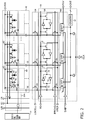
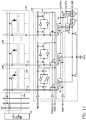
- FIG. 2 is a more specific circuit diagram of the pixel driving circuit 20, the pixel array 30, and the readout circuit 60 illustrated in FIG. 1 .
- the solid-state image sensor 100 includes a plurality of readout wires 32 and a load circuit 34.
- the plurality of readout wires 32 correspond to the respective columns of the pixel cells 40, and connect the pixel cells 40 to the readout circuit 60.
- the load circuit 34 includes a plurality of load transistors 35 respectively connected to the readout wires 32.
- Each of the pixel cells 40 includes an avalanche photodiode (APD) 41, a floating diffusion (FD) 42, a pixel reset transistor 43, a transfer transistor 44, an amplifying transistor 45, and a selecting transistor 46.
- a substrate voltage VSUB is applied to an anode of the APD 41.
- the substrate voltage VSUB is, for example, -20 V.
- the APD 41 collects charges in a cathode thereof until quenching. That is, the APD 41 detects, by photoelectric conversion, a photon which has entered the APD 41. More specifically, in a state where a large negative bias VSUB is applied to the anode of the APD 41, when one photon enters, avalanche multiplication occurs by photoelectric conversion, and the APD 41 collects charges whose amount reaches a saturation charge amount to the cathode of the APD 41. At this time, the APD 41 operates in a Geiger mode.
- FIG. 3 is a cross-sectional view illustrating an example configuration of the avalanche photodiode 41 illustrated in FIG. 2 .
- FIG. 3 shows a schematic cross-sectional view of the APD 41 and the transfer transistor 44 adjacent to the APD 41, in a cross section along the direction of the length of the transfer transistor 44.
- An optical filter 53 and a condenser lens 54 are formed on a protective film 52 on the back surface of a substrate 51.
- a region 55 of the substrate near the back surface is doped in a p type
- a region (front surface region) 56 near the front surface of the substrate is doped in an n type
- these two regions form a pn junction. While electrons generated by a photon which entered from the back surface travel in a high-electric field region formed by this pn junction, the number of electrons that reach the n-type front-surface region is significantly multiplied (typically multiplied to 10000 electrons) by avalanche multiplication.
- the transfer transistor 44 transfers these electrons to a floating diffusion (capacitance) 58 in accordance with a voltage of a gate 59 thereof.
- the pixel cells 40 are electrically isolated from each other by an isolator 57.
- the APD 41 is disposed in a photoelectric converter of a back-illuminated image sensor so that the area of a right-receiving area can be thereby increased.
- the transfer transistor 44 is connected between the cathode of the APD 41 and the FD 42. When being selected by the vertical scanner 22, the transfer transistor 44 is turned on and transfers charges of the APD 41 to the FD 42. The FD 42 accumulates charges transferred from the APD 41.
- the reset transistor 43 is connected between the APD 41 and a power supply of a voltage VDD, and resets potentials of the APD 41 and the FD 42.
- the gate and source of the amplifying transistor 45 are connected to the FD 42 and the drain of the selecting transistor 46, respectively.
- the drain of the amplifying transistor 45 is supplied with, for example, a power supply voltage VDD.
- the power supply voltage VDD is 3 V, for example.
- the source of the selecting transistor 46 is connected to the readout wires 32.
- the readout wire 32 is a signal wire common to a plurality of pixel cells 40 belonging to the same column.
- the amplifying transistor 45 outputs a current to the corresponding readout wire 32 in accordance with the potential of the FD 42.
- the gates of the transfer transistor 44, the reset transistor 43, and the selecting transistor 46 receive a transfer signal TN, a reset signal RT, and a selection signal from the vertical scanner 22, respectively.
- the transfer transistor 44 transfers a detection result of the photon by the APD 41 to the corresponding readout wire 32 by way of the amplifying transistor 45 and the selecting transistor 46.
- the voltage of each readout wire 32 changes depending on the detection result of the photon.
- the readout wires 32 are connected to the load transistors 35, and the load transistors 35 constitute source followers together with the amplifying transistor 45 through the readout wires 32.
- the readout circuit 60 includes a column amplifier array 64, a horizontal transfer circuit 66, and a counter 67.
- the column amplifier array 64 includes a column amplifier 70 and a precharge circuit 76 for each of the readout wires 32.
- the column amplifier 70 includes inverters 71 and 72 and transistors 73 and 74.
- the precharge circuit 76 includes a precharge transistor.
- the precharge circuit 76 precharges the corresponding readout wire 32 with a precharge voltage.
- the column amplifier 70 includes a bistable circuit constituted by the inverters 71 and 72, and changes the voltage of the corresponding readout wire 32 to a logical high or low voltage and holds the voltage. That is, for each of the plurality of pixel cells 40 of the pixel array 30, the column amplifier 70 of the readout circuit 60 determines whether a photon is detected or not based on the voltage of the readout wire 32 corresponding to the pixel cell 40, changes the voltage of the readout wire 32 to one of the logical high or low voltages associated with a determination result, and holds the resulting voltage.
- the horizontal transfer circuit 66 sequentially transfers voltages of the readout wires 32 in response to a clock CLK, and outputs the transferred voltage as a determination result PXV indicating whether a photon is detected or not.
- the counter 67 is reset at each readout of a frame, increases a count value CNT in response to the clock CLK, and outputs the increased count value CNT.
- the count value CNT is associated with an address indicating a position of each pixel cell 40 in the pixel array 30. That is, for each of the pixel cells 40, the readout circuit 60 sequentially outputs a determination result on whether a photon is detected or not and an address indicating the position of the pixel cell 40.
- the solid-state image sensor 100 repeats the operation described above while changing rows of the pixel cells 40 selected by the vertical scanner 22.
- the column amplifier 70 may be a nonlinear circuit using the inverters 71 and 72. The use of the column amplifier 70 described above enables a signal from each pixel cell to be read out at higher speed.
- the solid-state image sensor 100 has a configuration similar to that of the typical CMOS image sensor.
- the pixel cells 40 of the solid-state image sensor 100 include none of a circuit for determining whether a photon is detected or not, a circuit for holding a determination result, and a circuit for counting and holding the number of photons.
- the circuit scale of the pixel cells 40 is substantially equal to that of the typical CMOS sensor. This enables miniaturization of pixel cells and reduction of power consumption. Since it is unnecessary to wait for entry of a plurality of photons, the time necessary for signal readout operation is short, and the speed of readout operation can be increased in the entire solid-state image sensor 100.
- FIG. 4 is a circuit diagram illustrating an example of an output circuit that may be included in the readout circuit 60 illustrated in FIG. 2 .
- the readout circuit 60 may further include an output circuit illustrated in FIG. 4 .
- the output circuit illustrated in FIG. 4 includes an AND circuit 61.
- the AND circuit 61 outputs a count value CNT of the counter 67 as a count value CNT2 without change only in a case where an output PXV of the horizontal transfer circuit 66 indicates detection of a photon. That is, only for a pixel cell 40 for which it is determined that a photon has been detected, the readout circuit 60 outputs an address indicating a position of this pixel cell 40 as a count value CNT2.
- the AND circuit 61 may output a count value CNT of the counter 67 as a count value CNT2 without change only in a case where the output PXV of the horizontal transfer circuit 66 does not indicate detection of a photon. In this case, only for a pixel cell 40 for which it is determined a photon has not been detected, the readout circuit 60 outputs an address indicating a position of this pixel cell 40 as a count value CNT2.
- FIG. 5 is a circuit diagram illustrating another example of the output circuit that may be included in the readout circuit 60 illustrated in FIG. 2 .
- the readout circuit 60 may further include the output circuit illustrated in FIG. 5 .
- the output circuit illustrated in FIG. 5 includes an AND circuit 61, a D flip-flop (DFF) 68, and an exclusive OR (XOR) circuit 69.
- the DFF 68 delays an output of the horizontal transfer circuit 66 by one clock and outputs the delayed output.
- the XOR circuit 69 outputs an exclusive OR XPV of an output of the horizontal transfer circuit 66 and the DFF 68.
- the AND circuit 61 outputs a count value CNT of the counter 67 as a count value CNT3 without change only in a case where the exclusive OR XPV is "1," that is, the output PXV of the horizontal transfer circuit 66 changes. That is, only in a case where a detection result of a photon for a specific pixel cell 40 is different from a detection result of a photon for a pixel cell adjacent to the specific pixel cell 40, the readout circuit 60 outputs an address indicating a position of the specific pixel cell 40 corresponding to an output of the horizontal transfer circuit 66 at this time, as a count value CNT3.
- the presence of the output circuit illustrated in FIG. 4 or 5 in the readout circuit 60 eliminates the necessity for reading data out of the solid-state image sensor 100 from all the pixel cells, and thus, the amount of data output by the readout circuit 60 can be reduced. Accordingly, it is possible to reduce the time necessary for reading out data from the solid-state image sensor 100.
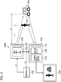
- FIG. 6 is a block diagram illustrating an example configuration of an imaging system according to this embodiment.
- An imaging system 1000 illustrated in FIG. 6 includes an imaging device (camera) 110, a light projection device 120, a controller 132, and a display 134.
- the imaging device 110 includes the solid-state image sensor 100, a light-receiving optical system 112, and a signal processor 116.
- the solid-state image sensor 100 is disposed at an image plane of the light-receiving optical system 112.
- the light projection device 120 includes a projection optical system 122 and a light source 124.
- the controller 132 outputs a timing adjustment signal to the solid-state image sensor 100 and the light source 124.
- the light source 124 of the light projection device 120 emits light in pulses with a predetermined period in response to the timing adjustment signal, and projects light to subjects 152 and 154.
- the projected light is reflected on each of the subjects 152 and 154.
- the reflected light is incident on the solid-state image sensor 100 through the light-receiving optical system 112.
- a photon after, for example, a time of 2 ⁇ L1/c from light emission of the light projection device 120 it is possible to know the distance to the subject 152.
- timings of light emission in the light projection device 120 and light reception in the solid-state image sensor 100 are adjusted based on a timing adjustment signal TC from the controller 132.
- FIG. 7 is a timing chart showing examples of signals in the solid-state image sensor 100 illustrated in FIG. 6 .
- each frame corresponds to one light exposure period.
- the solid-state image sensor 100 counts the number of frames of an output image from, for example, the start of taking the image, and outputs the number of frames as a frame number.
- a relationship between a frame number of each of a plurality of output frames and a time from an output of an optical pulse output to the light exposure period of the solid-state image sensor is set beforehand.
- the time from the output of the optical pulse to the light exposure period of the solid-state image sensor is expressed as photon fly times TF1, TF2, and TF3. More specifically, in this embodiment, relationships between a frame number and each of a light emission start time of the light source, a light exposure start time, and a light exposure end time are set beforehand.
- the photon flight time TF1 is, for example, a time from a light emission start time TL1 to a light exposure end time EE1.
- the photon flight time TF1 may be a time from the light emission start time TL1 to a light exposure start time ES1 or a time from the light emission start time TL1 to a time between the light exposure start time ES1 and the light exposure end time EE1. The same holds for the other photon flight times.
- the imaging system 1000 measures an average brightness of an imaging scene in an initialization period (not shown) before start of imaging. Based on a result of this measurement, the controller 132 controls the number of photons generated per an optical pulse of the light source 124 by a light control signal LC, and sets, at one, for example, an average of the number of photons which enter each pixel cell 40 of the solid-state image sensor 100 in the light exposure period of each frame.
- the controller 132 controls the number of photons generated per an optical pulse of the light source 124 by a light control signal LC, and sets, at one, for example, an average of the number of photons which enter each pixel cell 40 of the solid-state image sensor 100 in the light exposure period of each frame.
- the controller 132 controls the number of photons generated per an optical pulse of the light source 124 by a light control signal LC, and sets, at one, for example, an average of the number of photons which enter each pixel cell 40 of the solid-state image sensor 100 in the light exposure period
- the light source 124 emits light.
- the duration of the light emission period is, for example, 10 ns.
- a light exposure period starts. Only in a light exposure period corresponding to each frame, a negative bias VSUB is applied to the anodes of the APDs 41 in all the pixel cells 40.
- the light exposure period corresponding to a first frame is a period from the light exposure start time ES1 to the light exposure end time EE1. In this period, a photon enters the pixel cell 40. At the light exposure end time EE1, the transfer transistor 44 is turned on, and as described with reference to FIG. 2 , a detection result of the photon is output from the solid-state image sensor 100. In an output period DT1, detection results of photons for all the pixel cells 40 are sequentially output as an image of the first frame.
- the light source 124 emits light.
- a light exposure period corresponding to a second frame is a period from a light exposure start time ES2 to a light exposure end time EE2. In this period, no photon enters the pixel cell 40.
- the transfer transistor 44 is turned on, and as described with reference to FIG. 2 , a detection result of a photon is output from the solid-state image sensor 100.
- an output period DT2 detection results of photons for all the pixel cells 40 are sequentially output as an image of the second frame. Thereafter, similar operations are repeated.
- the frame number corresponds to a time (i.e., photon flight time) from an output of an optical pulse to a light exposure period of the solid-state image sensor.
- the duration of a photon flight time is set beforehand for each frame, and can be sequentially changed for each frame.
- a distance from the imaging system to a subject whose images can be taken can be changed.
- the signal processor 116 outputs an image from the solid-state image sensor 100 to the display 134.
- the display 134 displays an input image.
- the signal processor 116 may combine images of a plurality of frames output from the solid-state image sensor 100 and output the combined image.
- the signal processor 116 may combine images of frames corresponding to different photon flight times into one image, for example. In this case, the colors of the images may be different among the photon flight times.
- the signal processor 116 may reduce noise by, for example, averaging images of a plurality of frames corresponding to the same photon flight time.
- FIG. 8 is a timing chart showing examples of signals in a typical solid-state image sensor.
- the typical solid-state image sensor described above at every entry of a photon, information indicating the entry of the photon is accumulated in a circuit in a pixel cell. Readout is performed at every time a plurality of photons is received. That is, an interval of readout is long, and a timing of flight of each photon cannot be known.
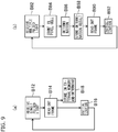
- Portion (a) of FIG. 9 is a flowchart depicting an example process in a solid-state image sensor according to this embodiment.
- the solid-state image sensor 100 receives single pulsed light in one frame period.
- the pulsed light is light with which the number of photons entering each pixel cell 40 is, for example, one in average.
- the solid-state image sensor 100 outputs light reception information to the outside of the solid-state image sensor 100 as image data corresponding to one frame.
- the image data is stored in an external memory as necessary, and used for processing such as determination of a pixel value, for example.
- initialization is performed, and similar operation is repeated subsequently.
- the solid-state image sensor 100 performs frame readout for each single pulse, and thus, the interval of frames is not affected by a processing speed of, for example, determination performed outside the sensor 100, and data can be read out at high speed.
- Portion (b) of FIG. 9 is a flowchart depicting an example process in a typical solid-state image sensor.
- the solid-state image sensor receives a plurality of beams of pulsed light in a block B82.
- a circuit in each pixel cell of the solid-state image sensor counts the number of photons by this pulsed light in a block B84, determines a pixel value based on whether the counted number reaches a threshold or not in a block B86, and then stores the determination result in a memory in a pixel in a block B88.
- the solid-state image sensor outputs light reception information to the outside of the solid-state image sensor as image data for one frame.
- a block B92 initialization is performed, and similar operation is repeated subsequently.
- counting and determination of a pixel value are performed in the pixel cells based on a plurality of photons.
- an interval between readouts is relatively long.
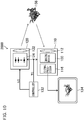
- FIG. 10 is a block diagram illustrating another example of the imaging system according to the embodiment.
- An imaging system 2000 illustrated in FIG. 10 is a system for detecting cell fluorescence, and is configured basically in the same manner as the imaging system 1000 illustrated in FIG. 6 . Thus, aspects similar to those of the imaging system 1000 will not be described.
- a controller 132 outputs a timing adjustment signal to a solid-state image sensor 100 and a light source 124.
- the light source 124 of a light projection device 120 emits light in pulses with a predetermined period in response to the timing adjustment signal, and projects the light to a cell sample 156 as a subject.
- Each pulsed light is absorbed in a light absorption group in the cell sample 156, and then, after a lapse of a specific time (lifetime) unique to the light absorption group, the light absorption group generates a fluorescent pulse.
- This fluorescent pulse enters the solid-state image sensor 100 through a light-receiving optical system 112.
- a photon included in the fluorescent pulse flies to the solid-state image sensor 100 with a delay of the lifetime.
- timings of light emission in the light projection device 120 and light reception in the solid-state image sensor 100 are adjusted based on a timing adjustment signal TC from the controller 132.
- the imaging system 2000 is different from the imaging system 1000 in obtaining an image corresponding to the lifetime of light absorption groups instead of a photon flight time.
- the frame number corresponds to a time from an output of an optical pulse to a light exposure period of the solid-state image sensor (i.e., the lifetime of the light absorption group).
- the duration of the lifetime is set beforehand for every frame, and can be sequentially changed for every frame. Depending on setting of the lifetime, the lifetime corresponding to the light absorption groups whose image can be taken from the imaging system can be changed.
- a signal processor 116 outputs an image from the solid-state image sensor 100 to a display 134.
- the display 134 displays an input image.
- the signal processor 116 may combine images of a plurality of frames output from the solid-state image sensor 100 and output the combined image.
- the signal processor 116 may combine images of frames corresponding to different lifetimes into one image, for example. In this case, the colors of the images may be made different among the lifetimes.
- the signal processor 116 may reduce noise by, for example, averaging images of a plurality of frames corresponding to the same lifetime.
- FIG. 11 is a circuit diagram illustrating another example configuration of the solid-state image sensor 100 illustrated in FIG. 1 .
- a solid-state image sensor 200 illustrated in FIG. 11 includes a pixel array 230 and a readout circuit 260 instead of the pixel array 30 and the readout circuit 60, and is configured in the same manner as the solid-state image sensor 100 except for including no load circuit 34.
- the pixel array 230 includes a plurality of pixel cells 240 arranged in rows and columns, for example.
- the readout circuit 260 includes the circuit illustrated in FIG. 5 in addition to the readout circuit 60.
- Each of the pixel cells 240 includes an avalanche photodiode (APD) 41 and a transfer transistor 44.
- APD avalanche photodiode
- the APD 41 multiplies, by a bias electric field, electron-hole pairs generated by entry of a photon to a number (typically 100,000) sufficient for detecting the photon.
- the transfer transistor 44 is connected between a cathode of the APD 41 and a corresponding readout wire 32. When being selected by the vertical scanner 22, the transfer transistor 44 is turned on and transfers charges of the APD 41 to the readout wire 32.
- the APD 41 outputs charges in an amount sufficient for detecting the photon, and thus, the transfer transistor 44 transfers charges of the APD 41 directly to the readout wire 32.
- the solid-state image sensor 200 is similar to the solid-state image sensor 100 described with reference to FIGS. 2 and 5 , and thus, description thereof will not be repeated.
- the solid-state image sensor 200 transfers charges of the APDs 41 directly to the readout wires 32, the amplifying transistors 45 are not needed.
- the APDs 41 are reset by the precharge circuits 76, and thus, the reset transistors 43 are not needed, either. Accordingly, in the solid-state image sensor 200, the pixel cells 240 can be further miniaturized, and power consumption can also be reduced.
- the solid-state image sensor 200 may not include an AND circuit 61, a DFF 68, and an XOR circuit 69.
- the solid-state image sensor 200 may include the circuit illustrated in FIG. 4 , instead of the AND circuit 61, the DFF 68, and the XOR circuit 69.
- the solid-state image sensor 200 may be a photodetector including a single pixel cell instead of a pixel array.
- the solid-state image sensor 200 may be a photodetector including: a pixel cell; a pixel driving circuit configured to drive the pixel cell; and a readout wire for readout of an output from the pixel cell, where the pixel cell includes an avalanche photodiode configured to detect a photon by avalanche multiplication occurring when one photon enters, and a transfer transistor configured to transfer a detection result of the photon by the avalanche photodiode to the readout wire corresponding to the pixel cell, and for the pixel cell, the readout circuit determines whether a photon is detected or not based on a voltage of the readout wire corresponding to the pixel cell and outputs a detection result as a value of a pixel corresponding to the pixel cell.
- the pixel cell includes an avalanche photodiode configured to detect a photon by avalanche multiplication occurring when one photon enters, and a transfer transistor configured to transfer a detection result of the photon by
- the functional blocks herein can be typically implemented by hardware. Alternatively, a part or whole of the functional blocks may be implemented by software. For example, such functional blocks can be implemented by a processor and a program executable on the processor. In other words, each of the functional blocks herein may be implemented by hardware, software, or any combination of hardware and software.
- the present disclosure is useful for a solid-state image sensor and an imaging system, for example.
Landscapes
- Engineering & Computer Science (AREA)
- Multimedia (AREA)
- Signal Processing (AREA)
- Physics & Mathematics (AREA)
- Electromagnetism (AREA)
- Computer Networks & Wireless Communication (AREA)
- General Physics & Mathematics (AREA)
- Radar, Positioning & Navigation (AREA)
- Remote Sensing (AREA)
- Transforming Light Signals Into Electric Signals (AREA)
- Solid State Image Pick-Up Elements (AREA)
Applications Claiming Priority (2)
| Application Number | Priority Date | Filing Date | Title |
|---|---|---|---|
| JP2018167137 | 2018-09-06 | ||
| PCT/JP2019/034984 WO2020050362A1 (ja) | 2018-09-06 | 2019-09-05 | 固体撮像素子、撮像システム、固体撮像素子の駆動方法、及び光検出器 |
Publications (2)
| Publication Number | Publication Date |
|---|---|
| EP3848965A4 EP3848965A4 (de) | 2021-07-14 |
| EP3848965A1 true EP3848965A1 (de) | 2021-07-14 |
Family
ID=69722422
Family Applications (1)
| Application Number | Title | Priority Date | Filing Date |
|---|---|---|---|
| EP19857977.3A Withdrawn EP3848965A1 (de) | 2018-09-06 | 2019-09-05 | Bilderzeugendes festkörperelement, bilderzeugendes system, verfahren zum betrieb des bilderzeugenden festkörperelements, und fotodetektor |
Country Status (5)
| Country | Link |
|---|---|
| US (1) | US11290675B2 (de) |
| EP (1) | EP3848965A1 (de) |
| JP (1) | JP7117535B2 (de) |
| CN (1) | CN112585953B (de) |
| WO (1) | WO2020050362A1 (de) |
Families Citing this family (8)
| Publication number | Priority date | Publication date | Assignee | Title |
|---|---|---|---|---|
| JP2019075394A (ja) | 2017-10-12 | 2019-05-16 | ソニーセミコンダクタソリューションズ株式会社 | 固体撮像素子、および、電子装置 |
| US12205401B2 (en) * | 2020-02-06 | 2025-01-21 | Novatek Microelectronics Corp. | Readout integrated circuit |
| US11503241B2 (en) * | 2020-02-06 | 2022-11-15 | Novatek Microelectronics Corp. | Readout integrated circuit |
| JP6953595B1 (ja) * | 2020-09-09 | 2021-10-27 | 浜松ホトニクス株式会社 | 距離画像取得装置及び距離画像取得方法 |
| JP7602346B2 (ja) * | 2020-10-14 | 2024-12-18 | 浜松ホトニクス株式会社 | 光センサ |
| JP7663460B2 (ja) * | 2021-08-26 | 2025-04-16 | キヤノン株式会社 | 光電変換装置、撮像装置、制御方法、及びコンピュータプログラム |
| CN114966806A (zh) * | 2022-04-11 | 2022-08-30 | 苏州瑞派宁科技有限公司 | 亚像素成像方法、装置、成像设备、探测器及存储介质 |
| JP2024119405A (ja) * | 2023-02-22 | 2024-09-03 | キヤノン株式会社 | 撮像装置、撮像装置の制御方法、及びプログラム |
Family Cites Families (16)
| Publication number | Priority date | Publication date | Assignee | Title |
|---|---|---|---|---|
| US6821808B2 (en) * | 2002-08-23 | 2004-11-23 | Micron Technology, Inc. | CMOS APS with stacked avalanche multiplication layer which provides linear and logarithmic photo-conversion characteristics |
| US7858917B2 (en) * | 2003-05-02 | 2010-12-28 | Massachusetts Institute Of Technology | Digital photon-counting geiger-mode avalanche photodiode solid-state monolithic intensity imaging focal-plane with scalable readout circuitry |
| US7547872B2 (en) * | 2005-02-14 | 2009-06-16 | Ecole Polytechnique Federale De Lausanne | Integrated circuit comprising an array of single photon avalanche diodes |
| JP2009239668A (ja) | 2008-03-27 | 2009-10-15 | Victor Co Of Japan Ltd | 撮像装置とその信号処理方法 |
| WO2010073137A1 (en) * | 2008-12-22 | 2010-07-01 | Koninklijke Philips Electronics N.V. | Cmos imager with single photon counting capability |
| US9210350B2 (en) * | 2013-12-09 | 2015-12-08 | Omnivision Technologies, Inc. | Low power imaging system with single photon avalanche diode photon counters and ghost image reduction |
| KR102409952B1 (ko) * | 2014-04-07 | 2022-06-17 | 삼성전자주식회사 | 고해상도, 고프레임률, 저전력 이미지 센서 |
| EP3164683B1 (de) * | 2014-07-02 | 2023-02-22 | The John Hopkins University | Fotodetektionsschaltung |
| CN106716994B (zh) | 2014-09-19 | 2020-01-17 | 松下知识产权经营株式会社 | 固体摄像装置 |
| CN108293099B (zh) * | 2015-12-07 | 2020-07-14 | 松下知识产权经营株式会社 | 固体摄像装置以及固体摄像装置的驱动方法 |
| US11280918B2 (en) | 2015-12-16 | 2022-03-22 | Sony Corporation | Imaging element, driving method, and electronic device |
| JP6961392B2 (ja) * | 2017-05-24 | 2021-11-05 | キヤノン株式会社 | 固体撮像素子、撮像装置及び撮像方法 |
| JP6924085B2 (ja) * | 2017-06-27 | 2021-08-25 | キヤノン株式会社 | 光検出装置及び撮像システム |
| CN107449516B (zh) * | 2017-07-06 | 2019-07-23 | 东南大学 | 一种自适应探测模式的光子计数线阵读出电路及方法 |
| CN108391071B (zh) * | 2017-11-23 | 2020-04-14 | 南京邮电大学 | 一种采用二次相关双采样技术的spad阵列级读出电路 |
| JP7227777B2 (ja) * | 2019-02-04 | 2023-02-22 | キヤノン株式会社 | 撮像装置 |
-
2019
- 2019-09-05 CN CN201980051087.6A patent/CN112585953B/zh active Active
- 2019-09-05 US US17/274,133 patent/US11290675B2/en active Active
- 2019-09-05 EP EP19857977.3A patent/EP3848965A1/de not_active Withdrawn
- 2019-09-05 WO PCT/JP2019/034984 patent/WO2020050362A1/ja not_active Ceased
- 2019-09-05 JP JP2020541298A patent/JP7117535B2/ja active Active
Also Published As
| Publication number | Publication date |
|---|---|
| US20210368119A1 (en) | 2021-11-25 |
| US11290675B2 (en) | 2022-03-29 |
| JP7117535B2 (ja) | 2022-08-15 |
| WO2020050362A1 (ja) | 2020-03-12 |
| CN112585953A (zh) | 2021-03-30 |
| JPWO2020050362A1 (ja) | 2021-08-30 |
| EP3848965A4 (de) | 2021-07-14 |
| CN112585953B (zh) | 2024-05-14 |
Similar Documents
| Publication | Publication Date | Title |
|---|---|---|
| US11290675B2 (en) | Solid-state image sensor and imaging system | |
| US11943542B2 (en) | Imaging devices with single-photon avalanche diodes having sub-exposures for high dynamic range | |
| JP7145201B2 (ja) | フォトセンサーにおける高強度光を検出すること | |
| US9171985B2 (en) | Pixel circuit with controlled capacitor discharge time of flight measurement | |
| US8822900B2 (en) | Multi-mode photodetector | |
| US8274588B2 (en) | Solid-state imaging device, method for driving the same, and imaging device | |
| CN113224090A (zh) | 成像系统 | |
| US12044802B2 (en) | Photoelectric conversion device and photoelectric conversion system comprising a control unit to set a third exposure period and a.fourth exposure period on a basis of light value comparison based on signal charge during first and second exposure periods | |
| US20130248689A1 (en) | Time-delay integration imaging method and apparatus using a high-speed in-pixel analog photon counter | |
| WO2017104438A1 (ja) | 撮像素子および駆動方法、並びに電子機器 | |
| EP1580987A1 (de) | Festkörperabbildungsvorrichtung | |
| CN112526528B (zh) | 光检测器和距离测定装置 | |
| JP2020162109A (ja) | 光電変換装置、光電変換システム、および移動体 | |
| US7012238B2 (en) | Amplification-type solid-state image pickup device incorporating plurality of arrayed pixels with amplification function | |
| US20250220323A1 (en) | Solid-state imaging device | |
| US20240251183A1 (en) | Imaging element and ranging device |
Legal Events
| Date | Code | Title | Description |
|---|---|---|---|
| STAA | Information on the status of an ep patent application or granted ep patent |
Free format text: STATUS: THE INTERNATIONAL PUBLICATION HAS BEEN MADE |
|
| PUAI | Public reference made under article 153(3) epc to a published international application that has entered the european phase |
Free format text: ORIGINAL CODE: 0009012 |
|
| STAA | Information on the status of an ep patent application or granted ep patent |
Free format text: STATUS: REQUEST FOR EXAMINATION WAS MADE |
|
| 17P | Request for examination filed |
Effective date: 20210309 |
|
| A4 | Supplementary search report drawn up and despatched |
Effective date: 20210611 |
|
| AK | Designated contracting states |
Kind code of ref document: A1 Designated state(s): AL AT BE BG CH CY CZ DE DK EE ES FI FR GB GR HR HU IE IS IT LI LT LU LV MC MK MT NL NO PL PT RO RS SE SI SK SM TR |
|
| DAV | Request for validation of the european patent (deleted) | ||
| DAX | Request for extension of the european patent (deleted) | ||
| STAA | Information on the status of an ep patent application or granted ep patent |
Free format text: STATUS: THE APPLICATION IS DEEMED TO BE WITHDRAWN |
|
| 18D | Application deemed to be withdrawn |
Effective date: 20220111 |