EP3851889B1 - Dispositif et procédé de couplage optique - Google Patents
Dispositif et procédé de couplage optique Download PDFInfo
- Publication number
- EP3851889B1 EP3851889B1 EP21155588.3A EP21155588A EP3851889B1 EP 3851889 B1 EP3851889 B1 EP 3851889B1 EP 21155588 A EP21155588 A EP 21155588A EP 3851889 B1 EP3851889 B1 EP 3851889B1
- Authority
- EP
- European Patent Office
- Prior art keywords
- birefringent layer
- layer
- beams
- coupling device
- optical coupling
- Prior art date
- Legal status (The legal status is an assumption and is not a legal conclusion. Google has not performed a legal analysis and makes no representation as to the accuracy of the status listed.)
- Active
Links
Images



Classifications
-
- G—PHYSICS
- G02—OPTICS
- G02B—OPTICAL ELEMENTS, SYSTEMS OR APPARATUS
- G02B6/00—Light guides; Structural details of arrangements comprising light guides and other optical elements, e.g. couplings
- G02B6/24—Coupling light guides
- G02B6/26—Optical coupling means
- G02B6/27—Optical coupling means with polarisation selective and adjusting means
-
- G—PHYSICS
- G02—OPTICS
- G02B—OPTICAL ELEMENTS, SYSTEMS OR APPARATUS
- G02B6/00—Light guides; Structural details of arrangements comprising light guides and other optical elements, e.g. couplings
- G02B6/24—Coupling light guides
- G02B6/26—Optical coupling means
- G02B6/27—Optical coupling means with polarisation selective and adjusting means
- G02B6/2706—Optical coupling means with polarisation selective and adjusting means as bulk elements, i.e. free space arrangements external to a light guide, e.g. polarising beam splitters
-
- G—PHYSICS
- G02—OPTICS
- G02B—OPTICAL ELEMENTS, SYSTEMS OR APPARATUS
- G02B6/00—Light guides; Structural details of arrangements comprising light guides and other optical elements, e.g. couplings
- G02B6/24—Coupling light guides
- G02B6/26—Optical coupling means
- G02B6/27—Optical coupling means with polarisation selective and adjusting means
- G02B6/2746—Optical coupling means with polarisation selective and adjusting means comprising non-reciprocal devices, e.g. isolators, FRM, circulators, quasi-isolators
-
- G—PHYSICS
- G02—OPTICS
- G02B—OPTICAL ELEMENTS, SYSTEMS OR APPARATUS
- G02B6/00—Light guides; Structural details of arrangements comprising light guides and other optical elements, e.g. couplings
- G02B6/24—Coupling light guides
- G02B6/26—Optical coupling means
- G02B6/27—Optical coupling means with polarisation selective and adjusting means
- G02B6/2753—Optical coupling means with polarisation selective and adjusting means characterised by their function or use, i.e. of the complete device
- G02B6/2766—Manipulating the plane of polarisation from one input polarisation to another output polarisation, e.g. polarisation rotators, linear to circular polarisation converters
-
- G—PHYSICS
- G02—OPTICS
- G02B—OPTICAL ELEMENTS, SYSTEMS OR APPARATUS
- G02B6/00—Light guides; Structural details of arrangements comprising light guides and other optical elements, e.g. couplings
- G02B6/24—Coupling light guides
- G02B6/26—Optical coupling means
- G02B6/27—Optical coupling means with polarisation selective and adjusting means
- G02B6/2753—Optical coupling means with polarisation selective and adjusting means characterised by their function or use, i.e. of the complete device
- G02B6/2793—Controlling polarisation dependent loss, e.g. polarisation insensitivity, reducing the change in polarisation degree of the output light even if the input polarisation state fluctuates
-
- G—PHYSICS
- G02—OPTICS
- G02B—OPTICAL ELEMENTS, SYSTEMS OR APPARATUS
- G02B6/00—Light guides; Structural details of arrangements comprising light guides and other optical elements, e.g. couplings
- G02B6/24—Coupling light guides
- G02B6/26—Optical coupling means
- G02B6/30—Optical coupling means for use between fibre and thin-film device
-
- G—PHYSICS
- G02—OPTICS
- G02B—OPTICAL ELEMENTS, SYSTEMS OR APPARATUS
- G02B6/00—Light guides; Structural details of arrangements comprising light guides and other optical elements, e.g. couplings
- G02B6/24—Coupling light guides
- G02B6/26—Optical coupling means
- G02B6/34—Optical coupling means utilising prism or grating
-
- G—PHYSICS
- G02—OPTICS
- G02B—OPTICAL ELEMENTS, SYSTEMS OR APPARATUS
- G02B6/00—Light guides; Structural details of arrangements comprising light guides and other optical elements, e.g. couplings
- G02B6/24—Coupling light guides
- G02B6/42—Coupling light guides with opto-electronic elements
- G02B6/4201—Packages, e.g. shape, construction, internal or external details
- G02B6/4204—Packages, e.g. shape, construction, internal or external details the coupling comprising intermediate optical elements, e.g. lenses, holograms
- G02B6/4207—Packages, e.g. shape, construction, internal or external details the coupling comprising intermediate optical elements, e.g. lenses, holograms with optical elements reducing the sensitivity to optical feedback
- G02B6/4208—Packages, e.g. shape, construction, internal or external details the coupling comprising intermediate optical elements, e.g. lenses, holograms with optical elements reducing the sensitivity to optical feedback using non-reciprocal elements or birefringent plates, i.e. quasi-isolators
- G02B6/4209—Optical features
-
- G—PHYSICS
- G02—OPTICS
- G02B—OPTICAL ELEMENTS, SYSTEMS OR APPARATUS
- G02B6/00—Light guides; Structural details of arrangements comprising light guides and other optical elements, e.g. couplings
- G02B6/24—Coupling light guides
- G02B6/26—Optical coupling means
- G02B6/27—Optical coupling means with polarisation selective and adjusting means
- G02B6/2706—Optical coupling means with polarisation selective and adjusting means as bulk elements, i.e. free space arrangements external to a light guide, e.g. polarising beam splitters
- G02B6/2713—Optical coupling means with polarisation selective and adjusting means as bulk elements, i.e. free space arrangements external to a light guide, e.g. polarising beam splitters cascade of polarisation selective or adjusting operations
- G02B6/272—Optical coupling means with polarisation selective and adjusting means as bulk elements, i.e. free space arrangements external to a light guide, e.g. polarising beam splitters cascade of polarisation selective or adjusting operations comprising polarisation means for beam splitting and combining
-
- G—PHYSICS
- G02—OPTICS
- G02B—OPTICAL ELEMENTS, SYSTEMS OR APPARATUS
- G02B6/00—Light guides; Structural details of arrangements comprising light guides and other optical elements, e.g. couplings
- G02B6/24—Coupling light guides
- G02B6/26—Optical coupling means
- G02B6/27—Optical coupling means with polarisation selective and adjusting means
- G02B6/2753—Optical coupling means with polarisation selective and adjusting means characterised by their function or use, i.e. of the complete device
- G02B6/2773—Polarisation splitting or combining
-
- G—PHYSICS
- G02—OPTICS
- G02B—OPTICAL ELEMENTS, SYSTEMS OR APPARATUS
- G02B6/00—Light guides; Structural details of arrangements comprising light guides and other optical elements, e.g. couplings
- G02B6/24—Coupling light guides
- G02B6/42—Coupling light guides with opto-electronic elements
- G02B6/4201—Packages, e.g. shape, construction, internal or external details
- G02B6/4204—Packages, e.g. shape, construction, internal or external details the coupling comprising intermediate optical elements, e.g. lenses, holograms
- G02B6/4213—Packages, e.g. shape, construction, internal or external details the coupling comprising intermediate optical elements, e.g. lenses, holograms the intermediate optical elements being polarisation selective optical elements
-
- G—PHYSICS
- G02—OPTICS
- G02B—OPTICAL ELEMENTS, SYSTEMS OR APPARATUS
- G02B6/00—Light guides; Structural details of arrangements comprising light guides and other optical elements, e.g. couplings
- G02B6/24—Coupling light guides
- G02B6/42—Coupling light guides with opto-electronic elements
- G02B6/4201—Packages, e.g. shape, construction, internal or external details
- G02B6/4204—Packages, e.g. shape, construction, internal or external details the coupling comprising intermediate optical elements, e.g. lenses, holograms
- G02B6/4214—Packages, e.g. shape, construction, internal or external details the coupling comprising intermediate optical elements, e.g. lenses, holograms the intermediate optical element having redirecting reflective means, e.g. mirrors, prisms for deflecting the radiation from horizontal to down- or upward direction toward a device
Definitions
- the present disclosure relates to polarization-sensitive optical components.
- a photonic integrated circuit can receive light from an off-chip light source.
- the received light can have a polarization state that varies unpredictably over time. It is desirable to account for polarization of the received light in a manner that reduces the effect of the polarization variation.
- WO 2016/206537 A1 discloses a free-space optical coupling device having a birefringent layer which can split incident light into first and second beams, which are then deviated by a lens in order to impinge on a photonic chip bearing grating couplers for redirection of the beams into the photonic chip.
- the invention relates to an optical coupling device according to claim 1, and a corresponding method according to claim 15. It overcomes the drawbacks identified in the background art.
- An optical coupling device can receive light from an off-chip light source, split the received light into separate beams having orthogonal polarization states, and couple the separate beams into respective waveguides.
- the optical coupling device can use a geometry that orients the polarization states of the separate beams to be coplanar.
- the separate beams can have the same polarization state, such as TE or TM.
- the waveguides can direct the beams to a photonic integrated circuit that can operate on the beams, such as by applying gain. Because the beams have the same polarization state, the photonic integrated circuit can operate on the beams equally, such as applying a particular level of gain to the separate beams. This can overcome any differences in photonic integrated circuit response with respect to polarization state, which might otherwise cause one beam to be affected more than another. After the photonic integrated circuit has performed its function on the separate beams, the same optical coupling device or a different device can direct the beams away from the photonic integrated circuit.
- the optical coupling device can include multiple grating couplers that are spatially separated from each other. Such spatial separation can allow a dedicated grating coupler to be used for each beam in the device. Compared with using a single grating coupler for multiple beams, using dedicated grating couplers, each operating on just a single beam, can allow for more efficient coupler designs.
- an optical coupling device can include a first birefringent layer having opposing first and second surfaces.
- the first birefringent layer can split incident light received at the first surface into first and second beams.
- the first and second beams can have respective polarization orientations that are orthogonal to each other.
- the first birefringent layer can propagate the first and second beams along respective first and second paths within the first birefringent layer to the second surface.
- the first and second beams can be spatially separated at the second surface.
- a redirection layer facing the second surface of the first birefringent layer can include first and second grating couplers configured to respectively redirect the first and second beams to propagate within the redirection layer as respective third and fourth beams.
- the third and fourth beams can have respective polarization orientations that are parallel to each other.
- FIG. 1 shows an example of an optical coupling device 100, in accordance with some embodiments.
- Such an optical coupling device 100 can receive light from a light source, split the received light into separate beams having orthogonal polarization states, and direct the separate beams toward respective waveguides using a geometry that orients the polarization states of the directed beams to be coplanar.
- the optical coupling device 100 of FIG. 1 can also be used in reverse, to combine light from the respective waveguides.
- the configuration of FIG. 1 is but one example of an optical coupling device 100 that can perform such a function. Other configurations can also be used.
- FIG. 1 shows an edge view of a layered structure, which is cut along the lines on beams that propagate within the layered structure. It will be understood that the cut shown in FIG. 1 is strictly for clarity, and that the actual layers in the layered structure extend laterally beyond the cut shown in FIG. 1 .
- FIGS. 4 and 5 discussed below, also include views with cuts that are shown strictly for clarity.
- the optical coupling device 100 includes a first birefringent layer 102 that can separate orthogonal polarization components of a light beam. Separation of the polarization components occurs if the light beam strikes the first birefringent layer 102 at normal incidence (e.g., parallel to a surface normal of the first birefringent layer 102 ), or if the light beam strikes the first birefringent layer 102 at non-normal incidence (e.g., angled with respect to the surface normal).
- the first birefringent layer 102 has opposing first and second surfaces 104, 106. In some examples, the first birefringent layer 102 can define a longitudinal axis (LA) as being orthogonal to the first surface 104.
- the first birefringent layer 102 is formed from a material having an optic axis 108 that is angled with respect to the longitudinal axis (LA) by an angle between zero and ninety degrees, non-inclusive.
- the optic axis 108 can be angled at forty-five degrees with respect to the longitudinal axis (LA).
- the forty-five degree angular orientation of the optic axis 108 is a relatively common crystal cut for birefringent materials. Other angular orientations can also be used.
- the first birefringent layer 102 can split incident light received at the first surface 104 into a first beam 110 and a second beam 112, corresponding to an ordinary ray and an extraordinary ray.
- the first and second beams 110, 112 can have respective polarization orientations that are orthogonal to each other.
- the ordinary ray can have a polarization state orthogonal to a plane formed by the optic axis 108 and the longitudinal axis (LA).
- the extraordinary ray can have a polarization state orthogonal to both the polarization state of the ordinary ray and the propagation direction of the extraordinary ray.
- the polarization state of the extraordinary ray can lie within the plane formed by the optic axis 108 and the longitudinal axis (LA).
- the first birefringent layer 102 can propagate the first and second beams 110, 112 along respective first and second paths 114, 116 within the first birefringent layer 102 to the second surface 106.
- first and second paths 114, 116 are labeled in FIG. 1 with circled numerals 1 and 2, respectively.
- the first and second paths 114, 116 can be angled with respect to each other.
- the ordinary ray can continue on the same path as the incident light beam, while the extraordinary ray can angularly deflect toward or away from the optic axis 108.
- the extraordinary ray angularly deflects toward the optic axis 108.
- negative uniaxial birefringent materials such as calcite and lithium niobate
- the extraordinary ray angularly deflects away from the optic axis 108.
- the first birefringent layer 102 and any additional birefringent layers are formed from one or more positive uniaxial materials. It will be understood that negative uniaxial materials can alternatively be used for any or all of these birefringent layers.
- the angular deflection lies in the plane formed by the optic axis 108 and a longitudinal axis (LA) that is orthogonal to the first surface 104 of the first birefringent layer 102.
- the first and second beams 110, 112 can have a spatial separation at the second surface 106.
- the first birefringent layer 102 can include calcite, which has a relatively large birefringence.
- the first birefringent layer 102 can include calcite or lithium niobate, which are typically available in a wafer format from which pieces can be singulated to form the layered structure.
- the first birefringent layer 102 can include rutile, which is also typically available in wafers, and can optionally be deposited directly on a wafer of a photonic integrated circuit.
- the optical coupling device 100 can further include a redirection layer 118 facing the second surface 106 of the first birefringent layer 102.
- the redirection layer 118 can include first and second grating couplers 120, 122.
- the first and second grating couplers 120, 122 can each include a respective region in which a refractive index varies periodically.
- FIGS. 2 and 3 discussed below in further detail, show specific examples of first and second grating couplers 120, 122.
- either or both of the first and second grating couplers 120, 122 can be disposed on a surface of the redirection layer 118, such as on a top surface or a bottom surface of the redirection layer 118. In some examples, either or both of the first and second grating couplers 120, 122 can be disposed in a volume of the redirection layer 118, between the top and bottom surfaces of the redirection layer 118.
- first and second grating couplers 120, 122 can be spatially separated. In some examples, the first and second grating couplers 120, 122 can have a separation that matches a separation of the first and second beams 110, 112 at the second surface 106 of the first birefringent layer 102.
- the first and second grating couplers 120, 122 can respectively redirect the first and second beams 110, 112 to propagate within the redirection layer 118 as respective third and fourth beams 124, 126 along respective third and fourth paths 128, 130.
- the third and fourth paths 128, 130 are labeled in FIG. 1 with circled numerals 3 and 4, respectively.
- the third and fourth paths 128, 130 can be angled with respect to each other. In some examples, the third and fourth paths 128, 130 can be oriented orthogonal to the periodic variations of the first and second regions, respectively.
- the third and fourth beams 124, 126 can have respective polarization orientations that are coplanar. In some examples, the third and fourth beams 124, 126 can have respective polarization orientations that are parallel to the second surface 106 of the first birefringent layer 102.
- the third and fourth beams 124, 126 can have respective polarization orientations that are perpendicular to the second surface 106 of the first birefringent layer 102.
- the first grating coupler 120 can redirect the first beam 110 within a plane formed by the optic axis 108 of the first birefringent layer 102 and a longitudinal axis (LA) that is orthogonal to the first surface 104 of the first birefringent layer 102.
- the second grating coupler 122 can redirect the second beam 112 orthogonal to the plane formed by the optic axis 108 and the longitudinal axis (LA).
- the third and fourth beams 124, 126 can have respective polarization orientations that are parallel to the second surface 106 of the first birefringent layer 102.
- the grating coupler can redirect the first beam 110 orthogonal to the plane formed by the optic axis 108 and the longitudinal axis (LA).
- the grating coupler can redirect the second beam 112 within the plane formed by the optic axis 108 and the longitudinal axis (LA).
- the optical coupling device 100 can further include an optional spacer layer 132 positioned between the first birefringent layer 102 and the redirection layer 118.
- the spacer layer 132 can be formed as a substrate, upon which a photonic integrated circuit can be formed.
- the spacer layer 132 can be formed from an isotropic (e.g., non-birefringent) material.
- the spacer layer 132 can have a first surface 134 that contacts the second surface 106 of the first birefringent layer 102.
- the spacer layer 132 can have a second surface 136, opposite the first surface 134, which contacts the redirection layer 118.
- the optical coupling device 100 can be configured to couple light from an optical fiber to one or more waveguides.
- Such an optical fiber is not shown in FIG. 1 , but would be positioned at the top of the figure, oriented vertically, and emitting light into the optical coupling device 100.
- the light emitted from the optical fiber can have a central axis that is parallel to the longitudinal axis (LA).
- the light emitted from the optical fiber can have a central axis that is angled with respect to the longitudinal axis (LA).
- the waveguides are not shown in FIG. 1 , but would be positioned on or within the redirection layer 118, and oriented parallel to the redirection layer 118.
- Such coupling can be improved by using one or more elements in or on the optical coupling device 100 that change the collimation of the light.
- the optical coupling device 100 can optionally include a focusing layer 138 facing the first surface 104 of the first birefringent layer 102.
- the focusing layer 138 can impart a convergence onto the incident light to focus the third and fourth beams 124, 126 onto longitudinal ends of first and second waveguides, respectively.
- the convergence can impart a mode shape that efficiently couples the energy into waveguide modes, along the third and fourth paths 128, 130.
- the focusing layer 138 can include a first surface 140 that includes one or more curved features 142, and a second surface 144 contacting the first surface 104 of the first birefringent layer 102.
- the focusing layer 138 can include a lens.
- the lens can include optically isotropic materials, such as silica or air.
- the lens can include one or more surfaces. Each surface can have zero curvature (e.g., flat) or a finite curvature.
- the lens can be attached directly to a photonic integrated circuit, either on a substrate surface or on a surface that includes waveguides.
- a lens surface can be external to the photonic integrated circuit, separated by an air gap.
- birefringent material can be attached directly to the photonic integrated circuit.
- the lens and the birefringent material can be attached to one another but separated from the photonic integrated circuit by an air gap.
- the lens can be attached to the birefringent material, which is attached to the photonic integrated circuit.
- the first and second grating couplers 120, 122 can redirect the light beams without changing the convergence of the light beams.
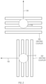
- FIG. 2 shows an example of first and second grating couplers 220, 222, in accordance with some embodiments.
- the first and second grating couplers 220, 222 can each include a respective region in which a refractive index varies periodically.
- the regions can be sized larger than respective footprints of the first and second beams 110, 112.
- the periodic variations of the first and second regions can be oriented orthogonal to the third and fourth paths 128, 130, respectively.
- the periodic variations in the first and second regions can be linear in shape.
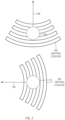
- FIG. 3 shows another example of first and second grating couplers 320, 322, in accordance with some embodiments.
- the first and second grating couplers 320, 322 can each include a respective region in which a refractive index varies periodically.
- the periodic variations of the first and second regions can be oriented orthogonal to the third and fourth paths 128, 130, respectively.
- the first and second grating couplers 320, 322 of FIG. 3 can include first and second regions that include periodic variations that are curved in shape.
- the periodic variations can curve toward the third and fourth paths 128, 130, respectively.
- Such curvature can impart the convergence onto the third and fourth beams 124, 126 along respective third and fourth paths 128, 130, so that the third and fourth beams 124, 126 can couple into first and second waveguides, respectively.
- the curvature can focus the third and fourth beams 124, 126 onto longitudinal ends of first and second waveguides, respectively.
- FIG. 4 shows an example of another optical coupling device 400, in accordance with some embodiments.
- Such an optical coupling device 400 can receive light from a light source, split the received light into separate beams having orthogonal polarization states, and direct the separate beams toward respective waveguides using a geometry that orients the polarization states of the directed beams to be coplanar.
- the optical coupling device 400 of FIG. 4 when used in reverse, can direct light from a third waveguide toward the light source. In this manner, the device of FIG. 4 can function as a combination polarization separator/optical circulator.
- the configuration of FIG. 4 is but one example of a combination polarization separator/optical circulator. Other configurations can also be used.
- the optical coupling device 400 can include a first birefringent layer 102 having opposing first and second surfaces.
- the first birefringent layer 102 can split incident light received at the first surface into first and second beams.
- the first and second beams can have respective polarization orientations that are orthogonal to each other.
- the first birefringent layer 102 can propagate the first and second beams along respective first and second paths within the first birefringent layer 102 to the second surface.
- the first and second paths can be angled with respect to each other.
- the first and second beams can have a spatial separation at the second surface.
- the optical coupling device 400 can include a redirection layer 118 facing the second surface of the first birefringent layer 102.
- the redirection layer 118 can include first and second grating couplers configured to respectively redirect the first and second beams to propagate within the redirection layer 118 as respective third and fourth beams along respective third and fourth paths.
- the third and fourth paths can be angled with respect to each other.
- the first birefringent layer 102, redirection layer 118, optional spacer layer 132, and optional focusing layer 138 can be identical in structure and function to the corresponding elements shown in FIG. 1 .
- the optical coupling device 400 of FIG. 4 includes additional elements, described below.
- the optical coupling device 400 can further include a second birefringent layer 402 having opposing first and second surfaces.
- the second surface of the second birefringent layer 402 can face the first surface of the first birefringent layer 102.
- the optic axis 408 of the second birefringent layer 402 is oriented parallel to the optic axis 108 of the first birefringent layer 102.
- the optic axis 408 of the second birefringent layer 402 can be angled with respect to the optic axis 108 of the first birefringent layer 102, which viewed along the longitudinal axis (LA).
- first birefringent layer 102 and the second birefringent layer 402 can be formed from the same birefringent material. In other examples, the first birefringent layer 102 and the second birefringent layer 402 can be formed from different birefringent materials.
- the optical coupling device 400 can further include a half wave plate 404 and a Faraday rotator 406 positioned between the first birefringent layer 102 and the second birefringent layer 402.
- the Faraday rotator 406 and half wave plate 404 can each be positioned to rotate a plane of polarization by forty-five degrees. For light propagating in one direction, the rotation adds, so that the Faraday rotator 406 and half wave plate 404, combined, rotate the plane of polarization by ninety degrees. For light propagating in an opposite direction, the rotation cancels, so that the Faraday rotator 406 and half wave plate 404, combined, leave the plane of polarization unchanged.
- the Faraday rotator 406 rotates the plane of polarization by forty-five degrees using a so-called right hand screw rule.
- the Faraday rotator 406 rotates the plane of polarization by forty-five degrees using a so-called left hand screw rule.
- the half wave plate 404 and the Faraday rotator 406 can rotate by ninety degrees a polarization orientation of light propagating from the first birefringent layer 102 to the second birefringent layer 402, but not of light propagating from the second birefringent layer 402 to the first birefringent layer 102.
- the half wave plate 404 and the Faraday rotator 406 can rotate by ninety degrees a polarization orientation of light propagating from the second birefringent layer 402 to the first birefringent layer 102, but not of light propagating from the first birefringent layer 102 to the second birefringent layer 402.
- the half wave plate 404 faces the second birefringent layer 402, and the Faraday rotator 406 faces the first birefringent layer 102.
- the positions of the half wave plate 404 and the Faraday rotator 406 can be swapped, so that the half wave plate 404 faces the first birefringent layer 102, and the Faraday rotator 406 faces the second birefringent layer 402.
- light for each beam in the redirection layer 118 is polarized parallel to a top surface of the redirection layer 118 (e.g., orthogonal to the longitudinal axis (LA)).
- a top surface of the redirection layer 118 e.g., orthogonal to the longitudinal axis (LA)
- Using light that is polarized in a single direction can help reduce or eliminate polarization dependent loss for a photonic integrated circuit that uses the light in the redirection layer 118.
- light for each beam in the redirection layer 118 can be polarized orthogonal to a top surface of the redirection layer 118 (e.g., parallel to the longitudinal axis (LA)).
- other polarization orientations can also be used.
- FIG. 5 shows an example of another optical coupling device 500, in accordance with some embodiments.
- Such an optical coupling device 500 can receive light from a light source, split the received light into separate beams having orthogonal polarization states, and direct the separate beams toward respective waveguides using a geometry that orients the polarization states of the directed beams to be coplanar.
- the optical coupling device 500 of FIG. 5 when used in reverse, can direct light from third and fourth waveguides toward the light source. In this manner, the device of FIG. 5 can function as a combination polarization separator/optical circulator.
- the configuration of FIG. 5 is but one example of a combination polarization separator/optical circulator. Other configurations can also be used.
- the optical coupling device 500 can include a first birefringent layer 102 having opposing first and second surfaces.
- the first birefringent layer 102 can split incident light received at the first surface into first and second beams.
- the first and second beams can have respective polarization orientations that are orthogonal to each other.
- the first birefringent layer 102 can propagate the first and second beams along respective first and second paths within the first birefringent layer 102 to the second surface.
- the first and second paths can be angled with respect to each other.
- the first and second beams can have a spatial separation at the second surface.
- the optical coupling device 500 can include a redirection layer 118 facing the second surface of the first birefringent layer 102.
- the redirection layer 118 can include first and second grating couplers configured to respectively redirect the first and second beams to propagate within the redirection layer 118 as respective third and fourth beams along respective third and fourth paths.
- the third and fourth paths can be angled with respect to each other.
- the first birefringent layer 102, redirection layer 118, optional spacer layer 132, and optional focusing layer 138 can be identical in structure and function to the corresponding elements shown in FIG. 1 .
- the optical coupling device 500 of FIG. 5 includes additional elements, described below.
- the optical coupling device 500 can further include a second birefringent layer 502 having opposing first and second surfaces.
- the second surface of the second birefringent layer 502 can face the first surface 104 of the first birefringent layer 102.
- the second birefringent layer 502 can have an optic axis 508 that is angled with respect to the longitudinal axis (LA).
- the second birefringent layer 502 can have an optic axis 508 that is angled at forty-five degrees with respect to the optic axis 108 of the first birefringent layer 102, when viewed along the longitudinal axis (LA).
- the optical coupling device 500 can further include a Faraday rotator 504 positioned between the first birefringent layer 102 and the second birefringent layer 502.
- the Faraday rotator 504 can rotate by forty-five degrees in a first direction a polarization orientation of light propagating from the first birefringent layer 102 to the second birefringent layer 502, and rotate by forty-five degrees, also in the first direction, a polarization orientation of light propagating from the second birefringent layer 502 to the first birefringent layer 102.
- light for each beam in the redirection layer 118 is polarized parallel to a top surface of the redirection layer 118 (e.g., orthogonal to the longitudinal axis (LA)).
- LA longitudinal axis
- Using light that is polarized in a single direction can help reduce or eliminate polarization dependent loss for a photonic integrated circuit that uses the light in the redirection layer 118.
- light for each beam in the redirection layer 118 can be polarized orthogonal to a top surface of the redirection layer 118 (e.g., parallel to the longitudinal axis (LA).
- other polarization orientations can also be used.
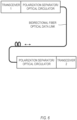
- FIG. 6 shows an example of a bidirectional optical link, in accordance with some embodiments.
- the bidirectional optical link includes two polarization separator/optical circulator components attached to two transceiver photonic integrated circuits, joined by an optical fiber.
- Other network architectures can also be used.
- An advantage to using the components as shown in FIG. 6 is that the optical fiber can direct light traveling in different directions in the fiber to different input and output ports on a photonic integrated circuit. This can reduce or remove crosstalk between the transmitted and received light path on the photonic integrated circuit.
- one or more grating couplers may be replaced with photodetectors. Such an arrangement would allow the photodetectors to measure the orthogonal polarizations of a polarization-multiplexed signal.
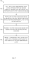
- FIG. 7 shows an example of a method of operation, in accordance with some embodiments, for an optical coupling device, such as devices from FIGS. 1 , 4 , and 5 .
- the method of FIG. 7 is but one example of a method of operation for an optical coupling device. Other suitable methods can also be used.
- the optical coupling device can split, with a first birefringent layer having opposing first and second surfaces, incident light received at the first surface into first and second beams.
- the first and second beams can have respective polarization orientations that are orthogonal to each other.
- the optical coupling device can propagate the first and second beams along respective first and second paths within the first birefringent layer to the second surface.
- the first and second paths can be angled with respect to each other.
- the first and second beams can have a spatial separation at the second surface.
- the optical coupling device can redirect the first and second beams with respective first and second grating couplers.
- the redirected first and second beams can propagate within a redirection layer facing the second surface of the first birefringent layer.
- the redirected first and second beams can propagate along respective third and fourth paths.
- the third and fourth paths can be angled with respect to each other.
- the optical coupling device can impart a convergence onto the incident light, with a focusing layer facing the first surface of the first birefringent layer, to focus the third and fourth beams onto longitudinal ends of first and second waveguides, respectively.
- an optical coupling device can include: a first birefringent layer having opposing first and second surfaces, the first birefringent layer configured to: split incident light received at the first surface into first and second beams, the first and second beams having respective polarization orientations that are orthogonal to each other, and propagate the first and second beams along respective first and second paths within the first birefringent layer to the second surface, the first and second paths being angled with respect to each other, the first and second beams having a spatial separation at the second surface; and a redirection layer facing the second surface of the first birefringent layer, the redirection layer including first and second grating couplers configured to respectively redirect the first and second beams to propagate within the redirection layer as respective third and fourth beams along respective third and fourth paths, the third and fourth paths being angled with respect to each other.
- Example 2 the optical coupling device of Example 1 can optionally be configured such that the first and second grating couplers are spatially separated.
- Example 3 the optical coupling device of any one of Examples 1-2 can optionally be configured such that the first grating coupler redirects the first beam within a plane formed by an optic axis of the first birefringent layer and a longitudinal axis that is orthogonal to the first surface of the first birefringent layer; the second grating coupler redirects the second beam orthogonal to the plane formed by the optic axis and the longitudinal axis; and the third and fourth beams have respective polarization orientations that are parallel to the second surface of the first birefringent layer.
- Example 4 the optical coupling device of any one of Examples 1-3 can optionally be configured such that the first and second grating couplers each include a respective region in which a refractive index varies periodically, the periodic variations of the first and second regions being oriented orthogonal to the third and fourth paths, respectively.
- the optical coupling device of any one of Examples 1-4 can optionally further include a focusing layer facing the first surface of the first birefringent layer, the focusing layer configured to impart a convergence onto the incident light to focus the third and fourth beams onto longitudinal ends of first and second waveguides, respectively.
- Example 6 the optical coupling device of any one of Examples 1-5 can optionally be configured such that the focusing layer includes a first surface that includes one or more curved features, and a second surface contacting the first surface of the first birefringent layer.
- Example 7 the optical coupling device of any one of Examples 1-6 can optionally be configured such that the first and second grating couplers include respective regions that include periodic variations that are curved in shape, the curvature configured to focus the third and fourth beams onto longitudinal ends of first and second waveguides, respectively.
- Example 8 the optical coupling device of any one of Examples 1-7 can optionally be configured such that the first birefringent layer defines a longitudinal axis as being orthogonal to the first surface; and the first birefringent layer is formed from a material having an optic axis that is angled with respect to the longitudinal axis by an angle between zero and ninety degrees, non-inclusive.
- Example 9 the optical coupling device of any one of Examples 1-8 can optionally be configured such that the optic axis is angled at forty-five degrees with respect to the longitudinal axis.
- Example 10 the optical coupling device of any one of Examples 1-9 can optionally further include a spacer layer positioned between the first birefringent layer and the redirection layer.
- Example 11 the optical coupling device of any one of Examples 1-10 can optionally be configured such that the spacer layer has a first surface that contacts the second surface of the first birefringent layer; and the spacer layer has a second surface, opposite the first surface, that contacts the redirection layer.
- the optical coupling device of any one of Examples 1-11 can optionally further include a second birefringent layer having opposing first and second surfaces, the second surface of the second birefringent layer facing the first surface of the first birefringent layer; and a half wave plate and a Faraday rotator positioned between the first birefringent layer and the second birefringent layer.
- Example 13 the optical coupling device of any one of Examples 1-12 can optionally be configured such that the half wave plate and the Faraday rotator are configured to rotate by ninety degrees a polarization orientation of light propagating from the first birefringent layer to the second birefringent layer, but not of light propagating from the second birefringent layer to the first birefringent layer.
- Example 15 the optical coupling device of any one of Examples 1-14 can optionally further include a second birefringent layer having opposing first and second surfaces, the second surface of the second birefringent layer facing the first surface of the first birefringent layer; and a Faraday rotator positioned between the first birefringent layer and the second birefringent layer.
- Example 16 the optical coupling device of any one of Examples 1-15 can optionally be configured such that the Faraday rotator is configured to: rotate by forty-five degrees in a first direction a polarization orientation of light propagating from the first birefringent layer to the second birefringent layer, and rotate by forty-five degrees in a second direction, opposite the first direction, a polarization orientation of light propagating from the second birefringent layer to the first birefringent layer.
- a method can include: splitting, with a first birefringent layer having opposing first and second surfaces, incident light received at the first surface into first and second beams, the first and second beams having respective polarization orientations that are orthogonal to each other; propagating the first and second beams along respective first and second paths within the first birefringent layer to the second surface, the first and second paths being angled with respect to each other, the first and second beams having a spatial separation at the second surface; and redirecting the first and second beams with respective first and second grating couplers, the redirected first and second beams propagating within a redirection layer facing the second surface of the first birefringent layer, the redirected first and second beams propagating along respective third and fourth paths, the third and fourth paths being angled with respect to each other.
- Example 18 the method of Example 17 can optionally further include imparting a convergence onto the incident light, with a focusing layer facing the first surface of the first birefringent layer, to focus the third and fourth beams onto longitudinal ends of first and second waveguides, respectively.
- an optical coupling device can include: a first birefringent layer having opposing first and second surfaces, the first birefringent layer configured to: split incident light received at the first surface into first and second beams, the first and second beams having respective polarization orientations that are orthogonal to each other, and propagate the first and second beams along respective first and second paths within the first birefringent layer to the second surface, the first and second paths being angled with respect to each other, the first and second beams having a spatial separation at the second surface; a redirection layer facing the second surface of the first birefringent layer, the redirection layer including spatially separated first and second grating couplers configured to respectively redirect the first and second beams to propagate within the redirection layer as respective third and fourth beams along respective third and fourth paths, the third and fourth paths being angled with respect to each other, the third and fourth beams having respective polarization orientations that are parallel to the second surface of the first birefringent layer; and a focusing
- the optical coupling device of Example 19 can optionally be configured such that the first birefringent layer defines a longitudinal axis as being orthogonal to the first surface; and the first birefringent layer is formed from a material having an optic axis that is angled at forty-five degrees with respect to the longitudinal axis.
Landscapes
- Physics & Mathematics (AREA)
- General Physics & Mathematics (AREA)
- Optics & Photonics (AREA)
- Optical Integrated Circuits (AREA)
- Optical Couplings Of Light Guides (AREA)
Claims (15)
- Dispositif de couplage optique (100, 400, 500), comprenant :
une première couche biréfringente (102) ayant des première et deuxième surfaces opposées (104, 106), la première couche biréfringente étant configurée pour :diviser la lumière incidente reçue sur la première surface selon un angle d'incidence normal par rapport à la première surface en des premier et deuxième faisceaux (110, 112), les premier et deuxième faisceaux ayant des orientations de polarisation respectives qui sont orthogonales l'une par rapport à l'autre, la première couche biréfringente ayant un axe optique selon un angle compris entre 0 et 90 degrés, non inclus, par rapport à la normale de la première surface, etpropager les premier et deuxième faisceaux le long de premier et deuxième trajets (114, 116) respectifs à l'intérieur de la première couche biréfringente jusqu'à la deuxième surface, les premier et deuxième trajets étant inclinés l'un par rapport à l'autre, les premier et deuxième trajets étant séparés dans l'espace au niveau de la deuxième surface ; etune couche de redirection (118) faisant face à la deuxième surface de la première couche biréfringente, les premier et deuxième faisceaux étant parallèles l'un à l'autre après avoir pénétré dans la couche de redirection et perpendiculaires à la deuxième surface de la première couche biréfringente, la couche de redirection comprenant un premier coupleur de réseau (120) configuré pour rediriger le premier faisceau à l'intérieur de la couche de redirection en tant que troisième faisceau le long d'un troisième trajet, la couche de redirection comprenant en outre un deuxième coupleur de réseau (122) configuré pour rediriger le deuxième faisceau à l'intérieur de la couche de redirection en tant que quatrième faisceau le long d'un quatrième trajet, les troisième et quatrième trajets étant parallèles à la deuxième surface de la première couche biréfringente et inclinés l'un par rapport à l'autre. - Dispositif de couplage optique selon la revendication 1, les premier et deuxième coupleurs de réseau étant spatialement séparés ; le premier coupleur de réseau redirigeant le premier faisceau orthogonalement pour se propager en tant que troisième faisceau le long du troisième trajet dans la couche de redirection, et le deuxième coupleur de réseau redirigeant le deuxième faisceau orthogonalement pour se propager en tant que quatrième faisceau le long du quatrième trajet dans la couche de redirection.
- Dispositif de couplage optique selon l'une quelconque des revendications 1 et 2 :le premier coupleur de réseau redirigeant le premier faisceau dans un plan formé par un axe optique de la première couche biréfringente et un axe longitudinal qui est orthogonal à la première surface de la première couche biréfringente ;le deuxième coupleur de réseau redirigeant le deuxième faisceau orthogonalement au plan formé par l'axe optique et l'axe longitudinal ; etles troisième et quatrième faisceaux ayant des orientations de polarisation respectives qui sont parallèles à la deuxième surface de la première couche biréfringente.
- Dispositif de couplage optique selon l'une quelconque des revendications 1 à 3, les premier et deuxième coupleurs de réseau comprenant chacun une région respective, dans laquelle un indice de réfraction varie périodiquement, les variations périodiques des première et deuxième régions étant orientées orthogonalement aux troisième et quatrième trajets, respectivement.
- Dispositif de couplage optique selon l'une quelconque des revendications 1 à 4, le dispositif de couplage optique comprenant en outre une couche de focalisation (138) faisant face à la première surface de la première couche biréfringente, la couche de focalisation étant configurée pour imprimer une convergence à la lumière incidente afin de focaliser les troisième et quatrième faisceaux sur des extrémités longitudinales des premier et deuxième guides d'ondes, respectivement ; la couche de focalisation comprenant une première surface qui comprend une ou plusieurs caractéristiques courbes, et une deuxième surface en contact avec la première surface de la première couche biréfringente.
- Dispositif de couplage optique selon l'une quelconque des revendications 1 à 5, les premier et deuxième coupleurs de réseau comprenant des régions respectives ayant des variations périodiques de forme incurvée, la courbure étant configurée pour focaliser les troisième et quatrième faisceaux sur des extrémités longitudinales de premier et deuxième guides d'ondes, respectivement.
- Dispositif de couplage optique selon l'une quelconque des revendications 1 ou 6 :la première couche biréfringente définissant un axe longitudinal orthogonal à la première surface ; etla première couche biréfringente étant formée d'un matériau dont l'axe optique est incliné par rapport à l'axe longitudinal d'un angle compris entre zéro et quatre-vingt-dix degrés, non inclus.
- Dispositif de couplage optique selon l'une quelconque des revendications 1 à 7, comprenant en outre une couche d'espacement positionnée entre la première couche biréfringente et la couche de redirection.
- Dispositif de couplage optique selon l'une quelconque des revendications 1 ou 8 :la couche d'espacement ayant une première surface en contact avec la deuxième surface de la première couche biréfringente ; etla couche d'espacement ayant une deuxième surface, opposée à la première surface, en contact avec la couche de redirection.
- Dispositif de couplage optique selon l'une quelconque des revendications 1 à 9, comprenant en outre :une deuxième couche biréfringente ayant des première et deuxième surfaces opposées, la deuxième surface de la deuxième couche biréfringente faisant face à la première surface de la première couche biréfringente ; etune plaque demi-onde et un rotateur de Faraday positionnés entre la première couche biréfringente et la deuxième couche biréfringente.
- Dispositif de couplage optique selon la revendication 10, la plaque demi-onde et le rotateur de Faraday étant configurés pour faire tourner de quatre-vingt-dix degrés une orientation de polarisation de la lumière se propageant de la première couche biréfringente à la deuxième couche biréfringente, mais pas de la lumière se propageant de la deuxième couche biréfringente à la première couche biréfringente.
- Dispositif de couplage optique selon la revendication 10, la plaque demi-onde et le rotateur de Faraday étant configurés pour faire tourner de quatre-vingt-dix degrés une orientation de polarisation de la lumière se propageant de la deuxième couche biréfringente à la première couche biréfringente, mais pas de la lumière se propageant de la première couche biréfringente à la deuxième couche biréfringente.
- Dispositif de couplage optique selon l'une quelconque des revendications 1 à 10, comprenant en outre :une deuxième couche biréfringente ayant des première et deuxième surfaces opposées, la deuxième surface de la deuxième couche biréfringente faisant face à la première surface de la première couche biréfringente ; etun rotateur de Faraday positionné entre la première couche biréfringente et la deuxième couche biréfringente.
- Dispositif de couplage optique selon la revendication 13, le rotateur de Faraday étant configuré pour :faire tourner de quarante-cinq degrés dans une première direction une orientation de polarisation de la lumière se propageant de la première couche biréfringente à la deuxième couche biréfringente, etfaire tourner de quarante-cinq degrés dans une deuxième direction, opposée à la première direction, une orientation de polarisation de la lumière se propageant de la deuxième couche biréfringente à la première couche biréfringente.
- Procédé, comprenant :la division, avec une première couche biréfringente ayant des première et deuxième surfaces opposées, de la lumière incidente reçue au niveau de la première surface selon un angle d'incidence normal par rapport à la première surface en des premier et deuxième faisceaux, les premier et deuxième faisceaux ayant des orientations de polarisation respectives orthogonales l'une à l'autre, la première couche biréfringente ayant un axe optique selon un angle compris entre 0 et 90 degrés, non inclus, par rapport à la normale de la première surface ;la propagation des premier et deuxième faisceaux le long des premier et deuxième trajets respectifs au sein de la première couche biréfringente jusqu'à la deuxième surface, les premier et deuxième trajets étant inclinés l'un par rapport à l'autre, les premier et deuxième faisceaux ayant une séparation spatiale au niveau de la deuxième surface ; etla redirection des premier et deuxième faisceaux avec des premier et deuxième coupleurs de réseau respectifs, les premier et deuxième faisceaux redirigés se propageant au sein d'une couche de redirection faisant face à la deuxième surface de la première couche biréfringente, les premier et deuxième faisceaux étant parallèles l'un à l'autre après être entrés dans la couche de redirection et perpendiculaires à la deuxième surface de la première couche biréfringente, les premier et deuxième faisceaux redirigés se propageant le long des troisième et quatrième trajets respectifs, les troisième et quatrième trajets étant parallèles à la deuxième surface de la première couche biréfringente et inclinés l'un par rapport à l'autre.
Applications Claiming Priority (3)
| Application Number | Priority Date | Filing Date | Title |
|---|---|---|---|
| US201662341195P | 2016-05-25 | 2016-05-25 | |
| PCT/US2017/034346 WO2017205553A1 (fr) | 2016-05-25 | 2017-05-24 | Dispositif et procédé de couplage optique |
| EP17728727.3A EP3465303B1 (fr) | 2016-05-25 | 2017-05-24 | Dispositif et procédé de couplage optique |
Related Parent Applications (1)
| Application Number | Title | Priority Date | Filing Date |
|---|---|---|---|
| EP17728727.3A Division EP3465303B1 (fr) | 2016-05-25 | 2017-05-24 | Dispositif et procédé de couplage optique |
Publications (3)
| Publication Number | Publication Date |
|---|---|
| EP3851889A1 EP3851889A1 (fr) | 2021-07-21 |
| EP3851889C0 EP3851889C0 (fr) | 2024-08-07 |
| EP3851889B1 true EP3851889B1 (fr) | 2024-08-07 |
Family
ID=59021593
Family Applications (2)
| Application Number | Title | Priority Date | Filing Date |
|---|---|---|---|
| EP21155588.3A Active EP3851889B1 (fr) | 2016-05-25 | 2017-05-24 | Dispositif et procédé de couplage optique |
| EP17728727.3A Active EP3465303B1 (fr) | 2016-05-25 | 2017-05-24 | Dispositif et procédé de couplage optique |
Family Applications After (1)
| Application Number | Title | Priority Date | Filing Date |
|---|---|---|---|
| EP17728727.3A Active EP3465303B1 (fr) | 2016-05-25 | 2017-05-24 | Dispositif et procédé de couplage optique |
Country Status (4)
| Country | Link |
|---|---|
| US (1) | US10151883B2 (fr) |
| EP (2) | EP3851889B1 (fr) |
| CN (2) | CN114859471B (fr) |
| WO (1) | WO2017205553A1 (fr) |
Families Citing this family (11)
| Publication number | Priority date | Publication date | Assignee | Title |
|---|---|---|---|---|
| JP6480880B2 (ja) * | 2016-03-16 | 2019-03-13 | 住友大阪セメント株式会社 | 光変調デバイス |
| EP3851889B1 (fr) | 2016-05-25 | 2024-08-07 | OpenLight Photonics, Inc. | Dispositif et procédé de couplage optique |
| US10551575B2 (en) * | 2017-08-24 | 2020-02-04 | Juniper Networks, Inc. | Optical coupler including a faraday rotator layer and at least one grating coupler |
| US10642125B1 (en) * | 2019-07-29 | 2020-05-05 | Globalfoundries Inc. | Optical beam steering with directionality provided by switched grating couplers |
| CN113267851A (zh) | 2019-12-23 | 2021-08-17 | 讯芸电子科技(中山)有限公司 | 光通讯模块 |
| EP4111246A1 (fr) * | 2020-02-26 | 2023-01-04 | Rheinisch-Westfälische Technische Hochschule (RWTH) Aachen | Coupleur optique comprenant un interposeur optique moulé conjointement avec un pic et 2 éléments sélectifs de polarisation permettant une isolation et/ou une gestion de polarisation |
| AU2021456934B2 (en) * | 2021-02-09 | 2024-11-21 | Oam Photonics Llc | Optical coherent imager having shared input-output path and method for sensing coherent light |
| JP7646244B2 (ja) * | 2021-07-21 | 2025-03-17 | オーエーエム・フォトニックス・リミテッド・ライアビリティー・カンパニー | 入出力経路を共有する光コヒーレントイメージャおよびコヒーレント光の感知方法 |
| JP7723258B2 (ja) * | 2021-08-31 | 2025-08-14 | 日亜化学工業株式会社 | 発光装置、およびディスプレイ |
| US20230236348A1 (en) * | 2022-01-21 | 2023-07-27 | Cisco Technology, Inc. | Focal polarization beam displacer |
| US11592540B1 (en) * | 2022-06-23 | 2023-02-28 | Ours Technology, Llc | LIDAR sensor system including a dual-polarization transmit and receive optical antenna |
Family Cites Families (14)
| Publication number | Priority date | Publication date | Assignee | Title |
|---|---|---|---|---|
| CN1154746A (zh) * | 1994-07-29 | 1997-07-16 | 宝丽来公司 | 对多束光进行光转换的器件 |
| US6014254A (en) | 1997-02-24 | 2000-01-11 | Cheng; Yihao | Optical device for splitting an input beam into two orthogonal polarization states |
| CA2344021C (fr) * | 2000-04-20 | 2010-01-26 | Jds Uniphase Inc. | Separateur ou coupleur de faisceaux polarises |
| US20020005987A1 (en) * | 2000-07-14 | 2002-01-17 | Gonzalo Wills | Polarization beam splitter or combiner |
| US6587273B2 (en) * | 2001-06-25 | 2003-07-01 | Jds Uniphase Corporation | Beam splitting device |
| US7035497B2 (en) * | 2002-10-25 | 2006-04-25 | Oplink Communications, Inc. | Miniature 1×2 magneto-optic switch |
| CN100392447C (zh) * | 2003-12-24 | 2008-06-04 | 招远招金光电子科技有限公司 | 低偏振相关损耗的宽范围内波长可调光学滤波器 |
| CN101881863A (zh) * | 2009-05-05 | 2010-11-10 | 菲尼萨光电通讯(上海)有限公司 | 梳状滤波器 |
| CN102681096A (zh) * | 2011-03-17 | 2012-09-19 | 昂纳信息技术(深圳)有限公司 | 一种偏振光干涉型的梳状滤波器 |
| CN104838299B (zh) * | 2013-09-09 | 2017-12-22 | 华为技术有限公司 | 光栅耦合器的光栅耦合方法、装置及系统 |
| US9935424B2 (en) * | 2015-04-01 | 2018-04-03 | Oracle International Corporation | Integrated laser with back-reflection isolator |
| US20160337041A1 (en) * | 2015-05-15 | 2016-11-17 | Futurewei Technologies, Inc. | Polarization Independent Reflective Modulator |
| US9927575B2 (en) * | 2015-06-25 | 2018-03-27 | Huawei Technologies Co., Ltd. | Optical coupling using polarization beam displacer |
| EP3851889B1 (fr) | 2016-05-25 | 2024-08-07 | OpenLight Photonics, Inc. | Dispositif et procédé de couplage optique |
-
2017
- 2017-05-24 EP EP21155588.3A patent/EP3851889B1/fr active Active
- 2017-05-24 EP EP17728727.3A patent/EP3465303B1/fr active Active
- 2017-05-24 WO PCT/US2017/034346 patent/WO2017205553A1/fr not_active Ceased
- 2017-05-24 CN CN202210474399.1A patent/CN114859471B/zh active Active
- 2017-05-24 CN CN201780031849.7A patent/CN109154700B/zh active Active
- 2017-05-24 US US15/604,603 patent/US10151883B2/en active Active
Also Published As
| Publication number | Publication date |
|---|---|
| EP3851889C0 (fr) | 2024-08-07 |
| EP3851889A1 (fr) | 2021-07-21 |
| CN109154700A (zh) | 2019-01-04 |
| WO2017205553A1 (fr) | 2017-11-30 |
| EP3465303A1 (fr) | 2019-04-10 |
| CN109154700B (zh) | 2022-06-03 |
| US10151883B2 (en) | 2018-12-11 |
| EP3465303B1 (fr) | 2021-03-10 |
| CN114859471A (zh) | 2022-08-05 |
| CN114859471B (zh) | 2024-11-15 |
| US20170343739A1 (en) | 2017-11-30 |
Similar Documents
| Publication | Publication Date | Title |
|---|---|---|
| EP3851889B1 (fr) | Dispositif et procédé de couplage optique | |
| US11668884B2 (en) | Optical coupler including a Faraday rotator layer and at least one grating coupler | |
| CN104583824B (zh) | 极化不同波长选择开关 | |
| US8570644B2 (en) | Optical modulator | |
| JP2001504947A (ja) | 光アイソレータ | |
| CN104838299B (zh) | 光栅耦合器的光栅耦合方法、装置及系统 | |
| JP5673283B2 (ja) | 偏波合成装置 | |
| JP2000111836A (ja) | ファラデ―回転子間に配置された複屈折くさびを有する光サ―キュレ―タあるいは光スイッチ | |
| CN102854564A (zh) | 一种具有对称结构的四端口光环行器 | |
| US6246518B1 (en) | Reflection type optical isolator | |
| US6546165B2 (en) | Optical multiplexing/demultiplexing module | |
| WO2014013640A1 (fr) | Séparateur de polarisation ainsi que procédé de fabrication de celui-ci, structure de séparation de polarisation, et mélangeur de lumière | |
| CN107561647A (zh) | 一种尾纤相互垂直的光隔离器 | |
| WO2005001548A1 (fr) | Isolateur optique en ligne | |
| JP7478755B2 (ja) | 偏光回転子 | |
| JP4293921B2 (ja) | 偏波無依存型多心光アイソレータ | |
| JP2004226599A (ja) | 偏光分離合成装置 | |
| KR20190115757A (ko) | 광 회로 소자 | |
| JP2013019963A (ja) | 光路切替装置および複数光信号の光路切替方法 | |
| CN100416339C (zh) | 一列形光隔离器 | |
| US20110273772A1 (en) | Beam splitter/combiner and method therefore | |
| JPH0886978A (ja) | 光サーキュレータおよび光の制御方法 | |
| JP2005148155A (ja) | 偏波無依存型光学装置 |
Legal Events
| Date | Code | Title | Description |
|---|---|---|---|
| PUAI | Public reference made under article 153(3) epc to a published international application that has entered the european phase |
Free format text: ORIGINAL CODE: 0009012 |
|
| STAA | Information on the status of an ep patent application or granted ep patent |
Free format text: STATUS: THE APPLICATION HAS BEEN PUBLISHED |
|
| AC | Divisional application: reference to earlier application |
Ref document number: 3465303 Country of ref document: EP Kind code of ref document: P |
|
| AK | Designated contracting states |
Kind code of ref document: A1 Designated state(s): AL AT BE BG CH CY CZ DE DK EE ES FI FR GB GR HR HU IE IS IT LI LT LU LV MC MK MT NL NO PL PT RO RS SE SI SK SM TR |
|
| STAA | Information on the status of an ep patent application or granted ep patent |
Free format text: STATUS: REQUEST FOR EXAMINATION WAS MADE |
|
| 17P | Request for examination filed |
Effective date: 20220117 |
|
| RBV | Designated contracting states (corrected) |
Designated state(s): AL AT BE BG CH CY CZ DE DK EE ES FI FR GB GR HR HU IE IS IT LI LT LU LV MC MK MT NL NO PL PT RO RS SE SI SK SM TR |
|
| RAP1 | Party data changed (applicant data changed or rights of an application transferred) |
Owner name: OPENLIGHT PHOTONICS, INC. |
|
| GRAP | Despatch of communication of intention to grant a patent |
Free format text: ORIGINAL CODE: EPIDOSNIGR1 |
|
| STAA | Information on the status of an ep patent application or granted ep patent |
Free format text: STATUS: GRANT OF PATENT IS INTENDED |
|
| RIC1 | Information provided on ipc code assigned before grant |
Ipc: G02B 6/30 20060101ALN20240214BHEP Ipc: G02B 6/27 20060101ALI20240214BHEP Ipc: G02B 6/42 20060101ALI20240214BHEP Ipc: G02B 6/34 20060101AFI20240214BHEP |
|
| INTG | Intention to grant announced |
Effective date: 20240301 |
|
| RIN1 | Information on inventor provided before grant (corrected) |
Inventor name: ROTH, JONATHAN EDGAR Inventor name: BAUTERS, JARED |
|
| GRAS | Grant fee paid |
Free format text: ORIGINAL CODE: EPIDOSNIGR3 |
|
| GRAA | (expected) grant |
Free format text: ORIGINAL CODE: 0009210 |
|
| STAA | Information on the status of an ep patent application or granted ep patent |
Free format text: STATUS: THE PATENT HAS BEEN GRANTED |
|
| AC | Divisional application: reference to earlier application |
Ref document number: 3465303 Country of ref document: EP Kind code of ref document: P |
|
| AK | Designated contracting states |
Kind code of ref document: B1 Designated state(s): AL AT BE BG CH CY CZ DE DK EE ES FI FR GB GR HR HU IE IS IT LI LT LU LV MC MK MT NL NO PL PT RO RS SE SI SK SM TR |
|
| REG | Reference to a national code |
Ref country code: GB Ref legal event code: FG4D |
|
| REG | Reference to a national code |
Ref country code: CH Ref legal event code: EP |
|
| REG | Reference to a national code |
Ref country code: DE Ref legal event code: R096 Ref document number: 602017084000 Country of ref document: DE |
|
| REG | Reference to a national code |
Ref country code: IE Ref legal event code: FG4D |
|
| U01 | Request for unitary effect filed |
Effective date: 20240829 |
|
| U07 | Unitary effect registered |
Designated state(s): AT BE BG DE DK EE FI FR IT LT LU LV MT NL PT RO SE SI Effective date: 20240910 |
|
| PG25 | Lapsed in a contracting state [announced via postgrant information from national office to epo] |
Ref country code: NO Free format text: LAPSE BECAUSE OF FAILURE TO SUBMIT A TRANSLATION OF THE DESCRIPTION OR TO PAY THE FEE WITHIN THE PRESCRIBED TIME-LIMIT Effective date: 20241107 |
|
| PG25 | Lapsed in a contracting state [announced via postgrant information from national office to epo] |
Ref country code: GR Free format text: LAPSE BECAUSE OF FAILURE TO SUBMIT A TRANSLATION OF THE DESCRIPTION OR TO PAY THE FEE WITHIN THE PRESCRIBED TIME-LIMIT Effective date: 20241108 Ref country code: PL Free format text: LAPSE BECAUSE OF FAILURE TO SUBMIT A TRANSLATION OF THE DESCRIPTION OR TO PAY THE FEE WITHIN THE PRESCRIBED TIME-LIMIT Effective date: 20240807 |
|
| PG25 | Lapsed in a contracting state [announced via postgrant information from national office to epo] |
Ref country code: IS Free format text: LAPSE BECAUSE OF FAILURE TO SUBMIT A TRANSLATION OF THE DESCRIPTION OR TO PAY THE FEE WITHIN THE PRESCRIBED TIME-LIMIT Effective date: 20241207 |
|
| PG25 | Lapsed in a contracting state [announced via postgrant information from national office to epo] |
Ref country code: HR Free format text: LAPSE BECAUSE OF FAILURE TO SUBMIT A TRANSLATION OF THE DESCRIPTION OR TO PAY THE FEE WITHIN THE PRESCRIBED TIME-LIMIT Effective date: 20240807 |
|
| PG25 | Lapsed in a contracting state [announced via postgrant information from national office to epo] |
Ref country code: RS Free format text: LAPSE BECAUSE OF FAILURE TO SUBMIT A TRANSLATION OF THE DESCRIPTION OR TO PAY THE FEE WITHIN THE PRESCRIBED TIME-LIMIT Effective date: 20241107 Ref country code: ES Free format text: LAPSE BECAUSE OF FAILURE TO SUBMIT A TRANSLATION OF THE DESCRIPTION OR TO PAY THE FEE WITHIN THE PRESCRIBED TIME-LIMIT Effective date: 20240807 |
|
| PG25 | Lapsed in a contracting state [announced via postgrant information from national office to epo] |
Ref country code: RS Free format text: LAPSE BECAUSE OF FAILURE TO SUBMIT A TRANSLATION OF THE DESCRIPTION OR TO PAY THE FEE WITHIN THE PRESCRIBED TIME-LIMIT Effective date: 20241107 Ref country code: PL Free format text: LAPSE BECAUSE OF FAILURE TO SUBMIT A TRANSLATION OF THE DESCRIPTION OR TO PAY THE FEE WITHIN THE PRESCRIBED TIME-LIMIT Effective date: 20240807 Ref country code: NO Free format text: LAPSE BECAUSE OF FAILURE TO SUBMIT A TRANSLATION OF THE DESCRIPTION OR TO PAY THE FEE WITHIN THE PRESCRIBED TIME-LIMIT Effective date: 20241107 Ref country code: IS Free format text: LAPSE BECAUSE OF FAILURE TO SUBMIT A TRANSLATION OF THE DESCRIPTION OR TO PAY THE FEE WITHIN THE PRESCRIBED TIME-LIMIT Effective date: 20241207 Ref country code: HR Free format text: LAPSE BECAUSE OF FAILURE TO SUBMIT A TRANSLATION OF THE DESCRIPTION OR TO PAY THE FEE WITHIN THE PRESCRIBED TIME-LIMIT Effective date: 20240807 Ref country code: GR Free format text: LAPSE BECAUSE OF FAILURE TO SUBMIT A TRANSLATION OF THE DESCRIPTION OR TO PAY THE FEE WITHIN THE PRESCRIBED TIME-LIMIT Effective date: 20241108 Ref country code: ES Free format text: LAPSE BECAUSE OF FAILURE TO SUBMIT A TRANSLATION OF THE DESCRIPTION OR TO PAY THE FEE WITHIN THE PRESCRIBED TIME-LIMIT Effective date: 20240807 |
|
| PG25 | Lapsed in a contracting state [announced via postgrant information from national office to epo] |
Ref country code: SM Free format text: LAPSE BECAUSE OF FAILURE TO SUBMIT A TRANSLATION OF THE DESCRIPTION OR TO PAY THE FEE WITHIN THE PRESCRIBED TIME-LIMIT Effective date: 20240807 |
|
| PG25 | Lapsed in a contracting state [announced via postgrant information from national office to epo] |
Ref country code: CZ Free format text: LAPSE BECAUSE OF FAILURE TO SUBMIT A TRANSLATION OF THE DESCRIPTION OR TO PAY THE FEE WITHIN THE PRESCRIBED TIME-LIMIT Effective date: 20240807 |
|
| PG25 | Lapsed in a contracting state [announced via postgrant information from national office to epo] |
Ref country code: SK Free format text: LAPSE BECAUSE OF FAILURE TO SUBMIT A TRANSLATION OF THE DESCRIPTION OR TO PAY THE FEE WITHIN THE PRESCRIBED TIME-LIMIT Effective date: 20240807 |
|
| U20 | Renewal fee for the european patent with unitary effect paid |
Year of fee payment: 9 Effective date: 20250416 |
|
| PLBE | No opposition filed within time limit |
Free format text: ORIGINAL CODE: 0009261 |
|
| STAA | Information on the status of an ep patent application or granted ep patent |
Free format text: STATUS: NO OPPOSITION FILED WITHIN TIME LIMIT |
|
| 26N | No opposition filed |
Effective date: 20250508 |
|
| REG | Reference to a national code |
Ref country code: CH Ref legal event code: H13 Free format text: ST27 STATUS EVENT CODE: U-0-0-H10-H13 (AS PROVIDED BY THE NATIONAL OFFICE) Effective date: 20251223 |
|
| PG25 | Lapsed in a contracting state [announced via postgrant information from national office to epo] |
Ref country code: CH Free format text: LAPSE BECAUSE OF NON-PAYMENT OF DUE FEES Effective date: 20250531 |
|
| GBPC | Gb: european patent ceased through non-payment of renewal fee |
Effective date: 20250524 |
|
| PG25 | Lapsed in a contracting state [announced via postgrant information from national office to epo] |
Ref country code: MC Free format text: LAPSE BECAUSE OF FAILURE TO SUBMIT A TRANSLATION OF THE DESCRIPTION OR TO PAY THE FEE WITHIN THE PRESCRIBED TIME-LIMIT Effective date: 20240807 |
|
| PG25 | Lapsed in a contracting state [announced via postgrant information from national office to epo] |
Ref country code: GB Free format text: LAPSE BECAUSE OF NON-PAYMENT OF DUE FEES Effective date: 20250524 |
|
| PG25 | Lapsed in a contracting state [announced via postgrant information from national office to epo] |
Ref country code: IE Free format text: LAPSE BECAUSE OF NON-PAYMENT OF DUE FEES Effective date: 20250524 |