EP3852496A1 - Mikrowellenbehandlungsvorrichtung - Google Patents
Mikrowellenbehandlungsvorrichtung Download PDFInfo
- Publication number
- EP3852496A1 EP3852496A1 EP19860278.1A EP19860278A EP3852496A1 EP 3852496 A1 EP3852496 A1 EP 3852496A1 EP 19860278 A EP19860278 A EP 19860278A EP 3852496 A1 EP3852496 A1 EP 3852496A1
- Authority
- EP
- European Patent Office
- Prior art keywords
- resonator
- patch
- microwave
- treatment chamber
- patch resonators
- Prior art date
- Legal status (The legal status is an assumption and is not a legal conclusion. Google has not performed a legal analysis and makes no representation as to the accuracy of the status listed.)
- Withdrawn
Links
Images


Classifications
-
- H—ELECTRICITY
- H05—ELECTRIC TECHNIQUES NOT OTHERWISE PROVIDED FOR
- H05B—ELECTRIC HEATING; ELECTRIC LIGHT SOURCES NOT OTHERWISE PROVIDED FOR; CIRCUIT ARRANGEMENTS FOR ELECTRIC LIGHT SOURCES, IN GENERAL
- H05B6/00—Heating by electric, magnetic or electromagnetic fields
- H05B6/64—Heating using microwaves
- H05B6/70—Feed lines
Definitions
- the present disclosure relates to a microwave treatment apparatus.
- microwaves radiated from a magnetron is supplied to a treatment chamber surrounded by metal walls so that a heating target, such as food, placed in the treatment chamber is dielectrically heated.
- Microwaves are repeatedly reflected on the walls of the treatment chamber.
- the phase of a reflected wave reflected on a metal wall shifts by 180 degrees with respect to an incident wave on the metal wall.
- the incident angle which is an angle between the reference line and the incident wave
- a reflection angle which is an angle between the reflected wave and the reference line.
- the size of the treatment chamber is sufficiently larger than the wavelength (about 120 mm) of microwaves in general. For this reason, a standing wave occurs in the treatment chamber due to the behaviors of the incident wave and the reflected wave at the metal wall.
- the standing wave has anti-nodes that constantly appear at locations with an intense electric field and nodes that constantly appear at locations with a weak electric field.
- the heating target is heated intensively when placed at a location where an anti-node of the standing wave appears, whereas the heating target is not so much heated when placed at a location where a node of the standing wave appears. This is a primary cause of uneven heating in the microwave oven.
- Possible methods for reducing such uneven heating caused by a standing wave and promoting even heating include a turn-table system of rotating a table to turn a heating target and a rotary antenna system of rotating an antenna for radiating microwaves.
- Non-Patent Literature 1 There is also proposed a technique that actively uses localized heating opposite to the even heating (see, for example, Non-Patent Literature 1).
- the device described in Non-Patent Literature 1 includes a plurality of microwave generators each constituted by a GaN semiconductor element, and supplies outputs of the microwave generators to a treatment chamber from various locations. Two supplied microwaves are provided with a phase difference so that microwaves are thereby concentrated on a heating target, thereby achieving localized heating.
- Non-Patent Literature 1 National Research and Development Agency, New Energy and Industrial Technology Development Organization et. al, "Development of industrial microwave heating system that uses GaN amplifier modules as heat sources," January 25, 2016
- one of the heating targets does not absorb all the microwaves even if the microwaves are intended to be focused on this heating target. Microwaves that have not been absorbed in that heating target enter the other heating target. Thus, it is difficult to perform localized heating on a plurality of heating targets as intended.
- a microwave treatment apparatus includes: a treatment chamber configured to accommodate a heating target; a microwave supply configured to supply microwaves to the treatment chamber; and a resonator unit having a resonance frequency in a frequency band of the microwaves.
- the resonator unit includes a plurality of patch resonator disposed such that at least three patch resonators are arranged along an orientation of a polarization plane generated on a metal wall constituting the treatment chamber.
- the microwave treatment apparatus of this aspect is capable of controlling a standing wave distribution in the treatment chamber, that is, a microwave energy distribution. As a result, in the case of heating a plurality of heating targets at simultaneously, the microwave treatment apparatus of this aspect is capable of adjusting microwave energy absorbed in each of the heating targets.
- a microwave treatment apparatus of a first aspect of the present disclosure includes: a treatment chamber configured to accommodate a heating target; a microwave supply configured to supply microwaves to the treatment chamber; and a resonator unit having a resonance frequency in a frequency band of the microwaves.
- the resonator unit includes a plurality of patch resonator disposed such that at least three patch resonators are arranged along an orientation of a polarization plane generated on a metal wall constituting the treatment chamber.
- the plurality of patch resonators are disposed such that the at least three patch resonators are arranged along each of a longitudinal axis and a lateral axis.
- the plurality of patch resonators include at least five square patch resonators arranged in a cross pattern.
- the plurality of patch resonators are disposed such that the at least three patch resonators are radially arranged along each of a longitudinal axis, a lateral axis, and an oblique axis.
- the patch resonator is a circular patch resonator.
- the microwave supply includes a microwave generator and a controller configured to control an oscillation frequency of the microwave generator.
- the resonator unit includes a plurality of resonator units having different resonance frequencies.
- the controller switches the resonator unit that oscillates among the plurality of resonator units by controlling the oscillation frequency.
- the resonator unit includes a plurality of resonator units.
- Each of the plurality of resonator units is disposed in a corresponding one of a plurality of divided regions on the metal wall constituting the treatment chamber.
- the plurality of resonator units have different resonance frequencies.
- each of the plurality of resonator units has a resonance frequency in accordance with an order in arrangement of the plurality of resonator units.
- each of the plurality of resonator units includes a conductor having a length in accordance with an order in arrangement of the plurality of resonator units.
- the microwave treatment apparatus is a microwave oven.
- the microwave treatment apparatus of the present disclosure is not limited to the microwave oven, and include, for example, a heat treatment apparatus, a chemical reaction treatment apparatus, and a semiconductor manufacturing apparatus, which utilize a dielectric heating process.
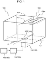
- FIG. 1 is a perspective view of microwave treatment apparatus 100 according to this exemplary embodiment.
- microwave treatment apparatus 100 includes treatment chamber 101 surrounded by metal walls, and microwave supply 160 configured to supply microwaves to treatment chamber 101.
- Microwave supply 160 includes waveguide 102, power feeder 103, microwave generator 104, and controller 105.
- Waveguide 102 has a rectangular-shaped cross section and transmits microwaves in a TE10 mode.
- Power feeder 103 is a waveguide opening formed in a connection portion between waveguide 102 and treatment chamber 101.
- the center of the waveguide opening is positioned at an intersection point of has center line L1 along the side-to-side axis and center line L2 along the forward and backward axis of treatment chamber 101 in FIG. 1 .
- the waveguide opening has a rectangular shape whose two sides are parallel to center lines L1 and L2.
- Controller 105 receives information on heating treatment, and causes microwave generator 104 to generate electric power having an output and a frequency based on the information.
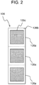
- FIG. 2 is a plan view illustrating a configuration of resonator unit 106. As illustrated in FIG. 2 , resonator unit 106 includes three square patch resonators 106a arranged in a 3 ⁇ 1 matrix pattern.
- Each square patch resonator 106a includes dielectric 106b and square conductor 106c.
- Square patch resonators 106a has a resonance frequency between 2.4 GHz to 2.5 GHz, which range is a frequency band of microwaves generated by microwave generator 104.
- FIGS. 3A and 3B are graphs showing frequency characteristics of a reflection phase generated by square patch resonators.
- the ordinate in FIG. 3A represents the reflection phase
- the ordinate in FIG. 3B represents an absolute value of the reflection phase.
- the phase of a reflection coefficient (hereinafter referred to as a reflection phase) of square patch resonator 106a seen from square conductor 106c varies from approximately +180 degrees to approximately -180 degrees in a frequency band of 2.4 GHz to 2.5 GHz.
- the resonance frequency of square patch resonator 106a is set at 2.45 GHz.
- FIG. 3B shows an absolute value of the ordinate of FIG. 3A .
- the reflection phase is 180 degrees at almost all the frequencies, but decreases to zero degrees near 2.45 GHz.
- the length of square conductor 106c is set at about a half of the wavelength of a current flowing in square conductor 106c, resonance occurs.
- the wavelength of microwaves at 2.45 GHz which is used in a typical microwave oven, is about 120 mm in the air having a dielectric constant of one.
- dielectric 106b has a dielectric constant close to 1 (one), for example, is foam polysthyrene
- the length of square conductor 106c is 53 mm, for example, resonance occurs.
- dielectric 106b If a general-purpose substrate material or resin material is selected for dielectric 106b, the dielectric constant is larger than one (about 2 to 5). With a large dielectric constant, the wavelength of microwaves tends to be short. Thus, square conductor 106c can be made short.
- the surface opposite to the patch surface, on which square conductor 106c of resonator unit 106 is disposed, has the same potential as the metal wall of treatment chamber 101.
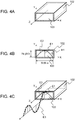
- FIGS. 4A through 4C are views for describing an electric field generated in a waveguide.
- FIG. 4A is a perspective view of the waveguide.
- FIG. 4B is a cross-sectional view of the waveguide when seen from the front of an opening.
- FIG. 4C is a view for describing an electric field radiated from the waveguide opening.
- Microwaves are transmitted by waveguide 102 in a positive direction of an Z axis shown in FIG. 4A , and are radiated from power feeder 103.
- width a of waveguide 102 is set at a value between 1/2 of wavelength ⁇ of microwaves to wavelength ⁇ of microwaves and height b of waveguide 102 is set at 1/2 of wavelength ⁇ of microwaves
- waveguide 102 transmits microwaves in the TE10 mode.
- an electric field represented by arrow E1 along the height axis occurs, and a magnetic field represented by arrow H1 along the width axis occurs.
- the electric field is at maximum at the center along the width axis in the waveguide 102, and is at zero at both ends in the waveguide 102. Accordingly, an electric field intensity distribution is represented as broken line E2.
- an electric field is radiated from power feeder 103 in a positive direction along the Z axis.
- a vector component of this electric field vibrates only along the Y axis (i.e., along the height axis of the waveguide) in a manner similar to that in arrow E1, and is transmitted along the Z axis with time. Accordingly, the electric field is transmitted as indicated by broken line E3.
- the electric field vector After having been radiated from waveguide 102, the electric field vector mainly vibrates only along the Y axis.
- This vibration direction of the electric field vector is called a polarized electromagnetic radiation, and a plane formed by the vibration direction and the transmission direction (i.e., YZ plane in this case) is called a polarization plane.
- the polarization plane is a plane (YZ plane) formed by the height axis (Y axis) and the transmission direction (Z axis) of the waveguide.
- microwaves radiated from waveguide 102 to treatment chamber 101 through power feeder 103 have a polarization plane represented by broken line E4 and formed by the vibration direction (direction of dot-dash line L1 in FIG. 1 ) and the transmission direction (upward direction in FIG. 1 ).
- microwaves are absorbed in the heating target in treatment chamber 101 while being repeatedly reflected on the metal walls.
- An electric field component in treatment chamber 101 is mainly generated only in a direction parallel to the polarization plane, and is hardly generated in other directions (e.g., direction L2 component in FIG. 1 ).
- resonator unit 106 is disposed including three square patch resonators 106a arranged along the polarization plane represented by broken line E4.
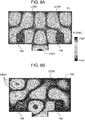
- FIG. 5 is a view showing characteristics of an electric field in treatment chamber 101 and a current vector on the patch surfaces of square patch resonators 106a in a case where the number and positions of square patch resonators 106a are changed.
- FIG. 5 shows, in the order from the top, an analytic model, an electric field on observation plane O1, an electric field on observation plane O2, and a current vector on the patch surfaces of square patch resonators 106a.
- the analytic models shown at the top row in FIG. 5 have configurations in each of which waveguide 102 is connected to treatment chamber 101, as in FIG. 1 . It should be noted that these analytic models are vertically inverted, as compared to the case of FIG. 1 .
- Observation plane O1 is a cross section at the center of treatment chamber 101 along the forward and backward axis, that is, a cross section along dot-dash line L2 in FIG. 1 , and is orthogonal to the polarization plane represented by broken line E4 in FIG. 1 .
- Observation plane O2 is located close to the left in treatment chamber 101, orthogonal to observation plane O1, and parallel to the polarization plane represented by dot-dash line L1 and broken line E4 in FIG. 1 .
- an electric field on observation plane O1 and an electric field on observation plane O2, for example, are shown in electric field intensity diagrams.
- current vectors on the patch surfaces of square patch resonators 106a are shown.
- the positions of square patch resonators 106a vary among the analytic models, and thus, current vectors on the patch surfaces are shown at positions (back, center, and front) corresponding to the positions of square patch resonators 106a. Isosceles triangles in the drawing represent orientations of the current vectors.
- analysis A square patch resonators 106a are not used.
- analysis B one square patch resonator 106a is disposed at the center along the forward and backward axis.
- analysis C one of two square patch resonators 106a is disposed at the back and the other at the front.
- analysis D one of three square patch resonators 106a is disposed at the back, another one at the center, and the last one at the front.
- observation plane O2 is disposed close to the left.
- a location where an anti-node of a standing wave occurs is selected on the bottom surface of treatment chamber 101 of the analytic model. In FIG. 5 , location 111 is selected.
- observation plane O2 A plane passing through location 111 on observation plane O1 and orthogonal to observation plane O1 is set as observation plane O2. With reference to an electric field distribution on observation plane O2 at this time, an anti-node of the standing wave occurs at location 112 as an intersection point of observation plane O1 and observation plane O2.
- the electric field distribution on each of observation plane O1 and observation plane O2 are bilaterally symmetric.
- An electric field at location 111 is intense, electric fields at location 113 and location 114 are weak, and an electric field at location 112 is about a middle between the electric fields at location 111 and location 113.
- the electric fields at location 111 and location 112 are weak.
- a node of the standing wave occurs at location 112 on observation plane O2.
- the electric field on observation plane O1 is not bilaterally symmetric any more.
- one square patch resonator 106a is disposed at the center in the forward and backward axis on observation plane O2. That is, in analysis B, one square patch resonator 106a is disposed at a location corresponding to an anti-node of the standing wave in analysis A.
- a result of analysis B shows that square patch resonator 106a disposed at the location corresponding to the anti-node of the standing wave changes the anti-node of the standing wave to the node.
- the reflection phases of square patch resonators 106a with respect to a frequency of 2.45 GHz is approximately zero degrees. This means that the phase difference between an incident wave on the patch surface and a reflected wave from the patch surface is approximately zero degrees.
- the phase difference between an incident wave and a reflected wave on a typical metal wall is 180 degrees, it is shown that a standing wave distribution different from a normal distribution is formed near resonator unit 106.
- analysis C as in the case of analysis A, the electric fields at location 111 and location 112 are intense. The electric fields are weak at location 113 and location 114 where square patch resonators 106a are disposed. In analysis A, nodes of the standing wave occur at location 113 and location 114. Specifically, a result of analysis C shows that square patch resonators 106a disposed at nodes of the standing wave where electric fields are weak do not significantly affect standing wave distributions.
- analysis D the electric fields are weak at location 111 and location 112 and an intense electric field is generated in region 115.
- the bilateral symmetry on observation plane O1 is disturbed.
- a result of analysis D seems to show that the effect of analysis B and the effect of analysis C are combined.
- an intense electric field is generated in region 115. This is an effect unique to the case where three square patch resonators 106a are disposed.
- FIGS. 6A through 6C are views for describing a reason for arranging three square patch resonators 106a.
- FIG. 6A is a view for describing an electric field in a case where two separate square patch resonators are disposed in an intense electric field.
- FIG. 6B is a view for describing an electric field in an opposite direction generated when three square patch resonators are disposed.
- FIG. 6C is a view for describing that the intense electric field in FIG. 6B becomes a weak electric field.
- Two square patch resonators 106a in FIG. 6A correspond to two square patch resonators 106a shown in analysis B in FIG. 5 .
- current vectors 116 and 117 in the same direction are generated by intense electric field 119, and electric fields 120 and 121 in opposite directions are generated between two square patch resonators 106a.
- induction field 122 in the same direction as electric field 120, and induction field 123 in the same direction as electric field 121 are excited.
- current vector 118 in the opposite direction is generated by induction fields 122 and 123 in square patch resonator 106a at the middle. Accordingly, electric field 124 in the opposite direction that cancels intense electric field 119 occurs. Consequently, the intense electric field can be weakened by the electric fields in the opposite direction generated by three square patch resonators 106a.
- analysis B in FIG. 5 shows only the first effect that one square patch resonator 106a disposed at a position corresponding to the anti-node of the standing wave weaken the electric field.
- Analysis D in FIG. 5 shows that the second effect that three square patch resonators 106a weaken the electric field is combined with the first effect.
- analysis D shows the effect that electric fields near square patch resonators 106a are further weakened as compared to analysis B. It is conceivable that an electric field at a location away from square patch resonator 106a is relatively intensified as a result so that an intense electric field is generated in region 115.
- the second effect is that the electric field is weakened when square patch resonator 106a is disposed at a location corresponding to an anti-node of the standing wave, whereas the standing wave does not change even when square patch resonator 106a is disposed at a location corresponding to a node of the standing wave.
- FIG. 7 is a cross-sectional view of microwave treatment apparatus 100 in a state where two heating targets are accommodated.
- treatment chamber 101 includes mounting plate 107 disposed above power feeder 103.
- Mounting plate 107 is made of a material having a low dielectric loss.
- Heating targets 108 and 109 are mounted on mounting plate 107.
- microwave generator 104 supplies microwaves 110.
- FIGS. 8A and 8B are views showing electric field distributions in treatment chamber 101 illustrated in FIG. 7 .
- FIG. 8A shows an electric field distribution in a case where resonator unit 106 is not provided.
- FIG. 8B shows an electric field distribution in a case where resonator unit 106 is disposed on a right portion of the ceiling of treatment chamber 101.
- microwave treatment apparatus 100 of this exemplary embodiment includes treatment chamber 101 surrounded by the metal walls, microwave supply 160 configured to supply microwaves to treatment chamber 101, and resonator unit 106 having a resonance frequency in a frequency band of microwaves.
- Resonator unit 106 includes three patch resonators (square patch resonators 106a) arranged along the orientation of the polarization plane generated on the metal walls constituting treatment chamber 101.
- microwaves having a frequency near a resonance frequency are supplied to treatment chamber 101, microwaves are reflected on a surface of resonator unit 106 with a phase difference of approximately zero degrees.
- microwaves are reflected on the metal walls of treatment chamber 101 with a phase difference of 180 degrees. Accordingly, the direction of an electric field is reversed. As a result, a certain change occurs in a standing wave distribution appearing in treatment chamber 101.
- a change of a standing wave distribution appearing in treatment chamber 101 can be more distinct.
- the standing wave does not change. Specifically, when three square patch resonators 106a are disposed along the orientation of the polarization plane, nodes of the standing wave constantly occur at the locations corresponding to three square patch resonators 106a, irrespective of whether the locations of square patch resonators 106a are locations corresponding to anti-nodes or locations corresponding to nodes of the standing wave.
- a standing wave distribution in treatment chamber 101 that is, microwave energy distribution
- desired microwave energy can be absorbed in each of the heating targets.
- resonator unit 106 includes flat square patch resonators 106a. Accordingly, resonator unit 106 can be disposed with substantially no loss of an effective inner volume of treatment chamber 101.
- Square patch resonators 106a are disposed such that the patch surface faces the inside of treatment chamber 101 and the surface opposite to the patch surface has the same potential as the metal walls of treatment chamber 101. With this configuration, an effective inner volume of treatment chamber 101 can be sufficiently obtained.
- Three square patch resonators 106a are disposed on one of the metal walls constituting treatment chamber 101. Accordingly, a change of a standing wave distribution caused by resonator unit 106 can be easily predicted. As a result, the heating targets can be heated as intended.
- resonator unit 106 is disposed on a metal wall of treatment chamber 101 opposite to a metal wall of treatment chamber 101 on which power feeder 103 is disposed. Accordingly, a microwave energy distribution can be concentrated near power feeder 103. As a result, heating targets can be efficiently heated together with microwave energy from power feeder 103.
- Microwave supply 160 includes microwave generator 104, and controller 105 configured to control an oscillation frequency and an output of microwave generator 104. In this manner, a plurality of heating targets can be heated at the same time.
- Resonator unit 106 may include four or more square patch resonators 106a.
- the center position of the four or more patch resonators varies depending on a combination of three adjacent patch resonators out of the four or more patch resonators. This corresponds to the fact that a plurality of combinations substantially exists for the combination of three patch resonators.
- Microwave treatment apparatus 100 has basically the same configuration as that of the first exemplary embodiment except for resonator unit 106.
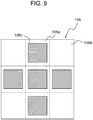
- FIG. 9 is a view illustrating a configuration of resonator unit 106 in this exemplary embodiment.
- resonator unit 106 includes square conductor 106c having a square shape.
- Supposing square conductor 106c includes nine regions divided into a 3 ⁇ 3 matrix pattern, dielectric 106b is provided in each of five regions included in the middle row and the middle column.
- Resonator unit 106 of this exemplary embodiment includes five square patch resonators 106a arranged in a cross pattern.
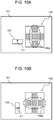
- FIGS. 10A and 10B are views illustrating examples of arrangement of resonator unit 106 and power feeder 103 on one metal wall (e.g., ceiling) of treatment chamber 101.
- power feeder 103 includes a laterally elongated waveguide opening.
- the vibration direction of electric field E1 is oriented along the longitudinal axis (upward and downward axis in FIG. 10A ), and the polarization plane is oriented along the longitudinal axis.
- three square patch resonators 106a arranged along the longitudinal axis out of five square patch resonators 106a arranged in a cross pattern function in a manner similar to resonator unit 106 of the first exemplary embodiment.
- power feeder 103 has a longitudinally elongated waveguide opening.
- the vibration direction of electric field E1 is oriented along the lateral axis (side-to-side axis in FIG. 10A ), and the polarization plane is oriented along the lateral axis.
- three square patch resonators 106a arranged along the lateral axis out of five square patch resonators 106a arranged in a cross pattern function in a manner similar to resonator unit 106 of the first exemplary embodiment.
- the longitudinal axis and the lateral axis correspond to the forward and backward axis and the side-to-side axis, respectively, of treatment chamber 101 in FIG. 1 .
- treatment chamber 101 has a laterally elongated rectangular solid shape and power feeder 103 is disposed in parallel with the outer shape of treatment chamber 101, as illustrated in FIGS. 10A and 10B .
- selection of the configuration illustrated in FIG. 10A or the configuration illustrated in FIG. 10B depends on design.
- resonator unit 106 has the configuration illustrated in FIG. 9
- resonator unit 106 functions in a manner similar to resonator unit 106 of the first exemplary embodiment in any of the configuration illustrated in FIG. 10A and the configuration illustrated in FIG. 10B .
- resonator unit 106 has five patch resonators (square patch resonators 106a) arranged in a cross pattern.
- anti-nodes of the standing wave can be changed to nodes for any of the polarization plane along the longitudinal axis and the polarization plane along the lateral axis.
- a standing wave distribution in treatment chamber 101 that is, a microwave energy distribution, can be controlled.
- resonator unit 106 includes five square patch resonators 106a arranged in a cross pattern. That is, resonator unit 106 includes the five patch resonators in total arranged such that three patch resonators are arranged along each of the longitudinal axis and the lateral axis. With this configuration, the number of necessary square patch resonators 106a can be reduced, as compared to a case where on resonator unit 106 of the first exemplary embodiment is provided along each of the longitudinal axis and the lateral axis.
- resonator unit 106 four or more square patch resonators 106a may be disposed along each of the longitudinal axis and the lateral axis.
- the center position of the four or more patch resonators varies depending on a combination of three adjacent patch resonators out of the four or more patch resonators. This corresponds to the fact that a plurality of combinations substantially exist for the combination of three patch resonators.
- FIG. 11 is a plan view illustrating a configuration of resonator unit 130 according to this exemplary embodiment.
- resonator unit 130 includes nine circular conductors 130c arranged on a circular dielectric 130b. Out of nine circular conductors 130c, one circular conductor 130c is disposed at the center, eight circular conductors 130c are arranged at regular intervals on a circumference about center circular conductor 130c. That is, in this configuration, three circular patch resonators 130a are arranged along each of the longitudinal axis, the lateral axis, and an oblique axis.
- the longitudinal axis and the lateral axis correspond to the forward and backward axis and the side-to-side axis, respectively, of treatment chamber 101 in FIG. 1 .
- the oblique axis is an axis forming 45 degrees with respect to each of the longitudinal axis and the lateral axis.
- the diameter of circular conductor 130c When the diameter of circular conductor 130c is set at a length of about a half of the wavelength of a current flowing on circular conductor 130c, resonance can be generated.
- the wavelength of microwaves at 2.45 GHz is about 120 mm in the air having a dielectric constant of one.
- dielectric 130b has a dielectric constant close to one, for example, is foam polysthyrene
- the diameter of circular conductor 130c is set at about 60 mm.
- a substrate having a dielectric constant of about 3.5, tan ⁇ of about 0.004, and a thickness of about 0.6 mm is used as dielectric 130b, and circular conductor 130c is formed in a copper foil pattern on the substrate.
- the diameter of resonator unit 130 can be reduced to 38 mm.
- FIG. 12A is a longitudinal cross-sectional view illustrating a configuration of microwave treatment apparatus 100 according to this exemplary embodiment.
- FIG. 12B is a transverse cross-sectional view taken along line 12B-12B in FIG. 12A .
- microwaves are not directly radiated from waveguide 102 to treatment chamber 101, but are radiated through radiation antenna 131 to treatment chamber 101.
- radiation antenna 131 includes coupling shaft 132 coupled to waveguide 102, and radiating unit 133.
- Radiating unit 133 has three walls (walls 134a, 134b, and 134c), flange 135 disposed around the walls, ceiling 136, and front opening 137.
- Radiation antenna 131 has a waveguide structure formed by walls 134a, 134b, and 134c and ceiling 136, and radiates microwaves in the direction represented by arrow 138 from front opening 137.
- microwave treatment apparatus 100 of this exemplary embodiment has a polarization plane including arrow 138 and perpendicular to the drawing sheet of FIG. 12B .
- Motor 139 is engaged with coupling shaft 132, and rotates coupling shaft 132 in response to an instruction from controller 105.
- radiating unit 133 rotates with the rotation of coupling shaft 132, orientation of microwaves radiated from front opening 137 and the polarization plane rotate.
- the polarization plane has various axes as well as the longitudinal axis and the lateral axis.
- resonator unit 130 having the configuration illustrated in FIG. 11 shows an effect on the polarization plane generated in the configurations of FIGS. 12A and 12B .
- FIG. 13A is a longitudinal cross-sectional view illustrating another configuration of microwave treatment apparatus 100 according to this exemplary embodiment.
- FIG. 13B is a transverse cross-sectional view taken along line 13B-13B in FIG. 13A .
- radiation antenna 131 has X-shaped circular polarized electromagnetic radiation aperture 140 provided on ceiling 136, and radiates microwaves of circular polarization from circular polarization aperture 140 upward in FIG. 13A .
- microwaves radiated from the waveguide opening generates an electric field having a single vibration direction. Since microwaves also has a transmission direction, a single polarization plane is generated in this case. Such microwaves are called microwaves of linear polarization.
- Resonator unit 130 having the configuration illustrated in FIG. 11 shows an effect on the polarization plane generated in the configurations of FIGS. 13A and 13B .
- resonator unit 130 includes one circular patch resonator 130a disposed at the center, and eight circular patch resonators 130a arranged at regular intervals on a circumference about the one circular patch resonator 130a.
- three patch resonators are arranged along each of the longitudinal axis, the lateral axis, and the oblique axis.
- resonator unit 130 functions in a manner similar to resonator unit 106 in the first exemplary embodiment.
- resonator unit 130 is constituted by circular patch resonators 130a including circular conductor 130c.
- the patch resonators whether resonance occurs or not depends on the length of the conductor.
- the circular conductor has a uniform length along all of the longitudinal, lateral, and oblique axes.
- resonator unit 130 allow resonance to occur on any of the longitudinal, lateral, and oblique polarization planes.
- a standing wave distribution in treatment chamber 101 that is, a microwave energy distribution, can be controlled.
- Resonator unit 130 of this exemplary embodiment is not limited to the configuration described above.
- resonator unit 130 may nine patch resonators arranged in a 3 ⁇ 3 matrix pattern. That is, in this exemplary embodiment, resonator unit 130 includes nine patch resonators in total in which three patch resonators are radially arranged along each of the longitudinal axis, the lateral axis, and the oblique axes.
- resonator unit 130 four or more circular patch resonators 130a may be arranged along each of longitudinal axis, the lateral axis, and the oblique axis.
- the center position of the four or more patch resonators varies depending on a combination of three adjacent patch resonators out of the four or more patch resonators. This corresponds to the fact that a plurality of combinations substantially exist for the combination of three patch resonators.
- FIG. 14 is a perspective view illustrating a configuration of microwave treatment apparatus 100 according to this exemplary embodiment.
- FIG. 15 is a view showing a characteristic of a resonator unit illustrated in FIG. 14 .
- microwave treatment apparatus 100 of this exemplary embodiment includes nine resonator units (resonator units 141, 142, 143, 144, 145, 146, 147, 148, and 149) arranged in a 3 ⁇ 3 pattern, on the ceiling of treatment chamber 101.
- Each of resonator units 141 through 149 includes nine circular conductors arranged in a 3 ⁇ 3 pattern on a square dielectric. With this configuration, nine patch resonators are formed in each of resonator units 141 through 149.
- Resonator units 141 through 149 have dielectrics having the same size. However, the diameter of a circular conductor included in a circular patch resonator of each resonator unit gradually increases in the order from resonator unit 141 to resonator unit 149. With this configuration, the resonance frequency of each resonator unit decreases by 10 MHz for each resonator unit in the order from resonator unit 141 to resonator unit 149.
- resonance frequencies of resonator units 141, 142, 143, 144, 145, 146, 147, 148 and 149 are 2.49 GHz, 2.48 GHz, 2.47 GHz, 2.46 GHz, 2.45 GHz, 2.44 GHz, 2.43 GHz, 2.42 GHz, and 2.41 GHz, respectively.
- the absolute value of a reflection phase is zero degrees at these resonance frequencies.
- a resonator unit in which resonance occurs is switched by controlling the frequency of microwaves to be supplied. For example, when microwaves at a frequency of 2.49 GHz are supplied, only resonator unit 141 resonates. Accordingly, an anti-node of the standing wave can be changed to a node near a left back region where resonator unit 141 is disposed. As a result, an electric field near the left back region can be weakened.
- an anti-node of the standing wave can be changed to a node near a left region where resonator units 141, 144, and 147 are disposed. Accordingly, an electric field in the left region can be weakened. In this case, an electric field in a right region is intensified, and as a result, heating target 109 disposed at the right can be strongly heated.
- resonator units 141 through 149 include circular patch resonators.
- resonator units 141 through 149 may include square patch resonators.
- Each of resonator units 141 through 149 may be resonator unit 130 in the third exemplary embodiment.
- a resonator unit in which resonance occurs is switched by controlling the frequency of microwaves to be supplied. Accordingly, an anti-node of the standing wave can be changed to a node near a resonator unit where resonance occurs. As a result, an electric field near the resonator unit where resonance occurs can be weakened.
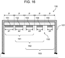
- FIG. 16 is a cross-sectional view illustrating a configuration of microwave treatment apparatus 100 according to this exemplary embodiment.
- microwave treatment apparatus 100 of this exemplary embodiment includes resonator unit 150 disposed on the ceiling of treatment chamber 101.
- Resonator unit 150 includes five conductors arranged at pitch P on a dielectric disposed on the ceiling of treatment chamber 101.
- patch resonators (patch resonators 151, 152, 153, 154, and 155) are formed.
- Conductors of five patch resonators have different lengths.
- the conductor of patch resonator 151 has length a1
- the conductor of patch resonator 152 has length a2
- the conductor of patch resonator 153 has length a3
- the conductor of patch resonator 154 has length a4, and the conductor of patch resonator 155 has length a5.
- Lengths a1 through a5 have a relationship of a1 > a2 > a3 > a4 > a5.
- each of patch resonators 151 through 155 includes a conductor having a length in accordance with the order in arrangement of patch resonators 151 through 155.
- each of patch resonators 151 through 155 has a resonance frequency in accordance with the order in arrangement of patch resonators 151 through 155.
- Combinations of three adjacent patch resonators out of these five patch resonators include left-end combination 161, center combination 162, and right-end combination 163.
- Combination 161 is constituted by patch resonators 151, 152, and 153.
- Combination 162 is constituted by patch resonators 152, 153, and 154.
- Combination 163 is constituted by patch resonators 153, 154, and 155.
- the average lengths of conductors of patch resonators included in these combinations become shorter from combination 161 to combination 163. Accordingly, in a case where three patch resonators included in combination 161 resonate at frequency f1, three patch resonators included in combination 162 resonate at frequency f2, and three patch resonators included in combination 163 resonate at frequency f3, frequencies f1 through f3 increase in this order.
- the length of the conductor of patch resonator 153 is set at approximately 1/2 of wavelength (effective length) of microwaves used in a typical microwave oven. Accordingly, frequency f2 can be set at 2.45 GHz, which is a frequency of these microwaves.
- the length of the conductor of patch resonator 152 is slightly longer than that of patch resonator 153, and the length of the conductor of patch resonator 151 is slightly longer than that of patch resonator 152.
- the length of the conductor of patch resonator 154 is slightly shorter than that of patch resonator 153, and the length of the conductor of patch resonator 155 is slightly shorter than that of patch resonator 154.
- the conducts of all the patch resonators have a length of approximately 1/2 of the wavelength (effective length) of microwaves.
- the length of the conductor of each patch resonator slightly varies.
- patch resonators located at ends in center combination 162 are shared by combinations 161 and 163 adjacent to combination 162.
- three combinations each constituted by three patch resonators can be formed by using five patch resonators, without using nine patch resonators.
- the combination of patch resonators where resonance occurs can be switched by setting the frequency of microwaves to be supplied at one of frequencies f1 through f3. Accordingly, an anti-node of the standing wave can be changed to a node near the combination of patch resonators where resonance occurs. As a result, an electric field near the combination of patch resonators where resonance occurs can be weakened.
- each of the three combinations each constituted by three patch resonators may correspond to one resonator unit. That is, it can be assumed that resonator unit 150 of this exemplary embodiment includes three resonator units.
- the patch surfaces of five patch resonators are constituted by copper foil applied onto a single surface of one substrate material.
- the surface of the substrate material opposite to the patch surface contacts the ceiling of treatment chamber 101.
- patch resonators 151, 152, 153, 154, and 155 can be disposed on the same single-sided substrate.
- Patch resonator units 151, 152, 153, 154, and 155 may be constituted by a double-sided substrate.
- the opposite surface can be made at the same potential as that of the metal surfaces of treatment chamber 101.
- a combination of patch resonators where resonance occurs can be switched by controlling the frequency of microwaves to be supplied. Accordingly, an anti-node of the standing wave can be changed to a node near the combination of patch resonators where resonance occurs. As a result, an electric field near the combination of patch resonators where resonance occurs can be weakened.
- resonator unit 150 is disposed only on the ceiling of treatment chamber 101.
- resonator unit 150 may be disposed on a side surface of treatment chamber 101.
- a localized standing wave distribution where an intense electric field occurs at the left of treatment chamber 101.
- a heating target placed at the left of treatment chamber 101 is more intensively heated.
- the use of the substrate as the dielectric of the resonator unit enables reduction of the size of the resonator unit.
- a loss may occur to generate heat or spark may occur between adjacent patches.
- a dielectric substrate may be used in the case of an apparatus requiring only microwaves with small energy for, for example, a chemical reaction treatment.
- another method may be employed in the case of an apparatus requiring microwaves with large energy for, for example, heating food.
- the second effect described with reference to FIGS. 6A through 6C is to weaken an intense electric potential caused by an unstable potential of the center one of the three patch resonators separated from the ground, by using an electric field in the opposite direction generated by the three patch resonators.
- switches are provided in all the patch resonators in order to effectively use the switches.
- the patch resonators are grounded by turning all the switches on so as not to cause the second effect.
- a standing wave distribution can be controlled as intended only by on/off control of the switches without controlling the frequency or by using resonator units having the same size.
- the present disclosure is applicable to a microwave treatment apparatus configured to perform heating treatment for, for example, food and/or a chemical reaction treatment, for example.
Landscapes
- Physics & Mathematics (AREA)
- Electromagnetism (AREA)
- Constitution Of High-Frequency Heating (AREA)
Applications Claiming Priority (2)
| Application Number | Priority Date | Filing Date | Title |
|---|---|---|---|
| JP2018168391 | 2018-09-10 | ||
| PCT/JP2019/035168 WO2020054608A1 (ja) | 2018-09-10 | 2019-09-06 | マイクロ波処理装置 |
Publications (2)
| Publication Number | Publication Date |
|---|---|
| EP3852496A1 true EP3852496A1 (de) | 2021-07-21 |
| EP3852496A4 EP3852496A4 (de) | 2021-12-01 |
Family
ID=69778039
Family Applications (1)
| Application Number | Title | Priority Date | Filing Date |
|---|---|---|---|
| EP19860278.1A Withdrawn EP3852496A4 (de) | 2018-09-10 | 2019-09-06 | Mikrowellenbehandlungsvorrichtung |
Country Status (4)
| Country | Link |
|---|---|
| EP (1) | EP3852496A4 (de) |
| JP (1) | JP7380221B2 (de) |
| CN (1) | CN111183708B (de) |
| WO (1) | WO2020054608A1 (de) |
Families Citing this family (3)
| Publication number | Priority date | Publication date | Assignee | Title |
|---|---|---|---|---|
| CN113038650B (zh) * | 2021-04-14 | 2022-09-06 | 西华师范大学 | 一种微波加热装置以及微波发射控制电路 |
| CN116941723A (zh) * | 2023-08-11 | 2023-10-27 | 上海蔚波微电子科技有限公司 | 一种食品处理设备及其方法 |
| CN119222586B (zh) * | 2024-12-03 | 2025-03-14 | 南京信息工程大学 | 一种具有谐振场波节谐振器的均匀微波加热装置 |
Family Cites Families (13)
| Publication number | Priority date | Publication date | Assignee | Title |
|---|---|---|---|---|
| JPH01213442A (ja) * | 1988-02-18 | 1989-08-28 | Asahi Chem Ind Co Ltd | ウォータージェットルームの製織方法 |
| FR2775552B1 (fr) * | 1998-02-27 | 2000-05-19 | Standard Products Ind | Dispositif de chauffage d'un materiau par micro-ondes |
| US6943330B2 (en) * | 2003-09-25 | 2005-09-13 | 3M Innovative Properties Company | Induction heating system with resonance detection |
| US7903040B2 (en) * | 2004-02-10 | 2011-03-08 | Telefonaktiebolaget L M Ericsson (Publ) | Tunable arrangements |
| ES2369312T3 (es) * | 2008-12-19 | 2011-11-29 | Whirlpool Corporation | Horno microondas que alterna entre modos predefinidos. |
| US20120175363A1 (en) * | 2010-12-30 | 2012-07-12 | Goji Limited | Rf-based pyrolytic cleaning |
| JP6558361B2 (ja) * | 2014-03-03 | 2019-08-14 | パナソニック株式会社 | 電磁界分布調整装置とその制御方法、およびマイクロ波加熱装置 |
| US10827568B2 (en) * | 2014-05-13 | 2020-11-03 | Centre National de la Recherche Scientifique—CNRS | Microwave oven |
| WO2017081855A1 (ja) * | 2015-11-10 | 2017-05-18 | パナソニック株式会社 | マイクロ波加熱装置 |
| EP3419383B1 (de) * | 2016-02-17 | 2021-07-07 | Panasonic Corporation | Mikrowellenheizvorrichtung |
| US10531526B2 (en) * | 2016-06-30 | 2020-01-07 | Nxp Usa, Inc. | Solid state microwave heating apparatus with dielectric resonator antenna array, and methods of operation and manufacture |
| WO2019009174A1 (ja) * | 2017-07-04 | 2019-01-10 | パナソニック株式会社 | マイクロ波処理装置 |
| CN108337758A (zh) * | 2018-02-05 | 2018-07-27 | 广东美的厨房电器制造有限公司 | 微波烹饪设备、微波加热控制方法和存储介质 |
-
2019
- 2019-09-06 WO PCT/JP2019/035168 patent/WO2020054608A1/ja not_active Ceased
- 2019-09-06 JP JP2019569855A patent/JP7380221B2/ja active Active
- 2019-09-06 EP EP19860278.1A patent/EP3852496A4/de not_active Withdrawn
- 2019-09-06 CN CN201980003759.6A patent/CN111183708B/zh active Active
Also Published As
| Publication number | Publication date |
|---|---|
| EP3852496A4 (de) | 2021-12-01 |
| JP7380221B2 (ja) | 2023-11-15 |
| CN111183708B (zh) | 2022-06-14 |
| CN111183708A (zh) | 2020-05-19 |
| WO2020054608A1 (ja) | 2020-03-19 |
| JPWO2020054608A1 (ja) | 2021-08-30 |
Similar Documents
| Publication | Publication Date | Title |
|---|---|---|
| KR101495378B1 (ko) | 마이크로파 가열 장치 | |
| US10356855B2 (en) | Microwave heating apparatus | |
| US10045403B2 (en) | Microwave heating device | |
| US9967925B2 (en) | RF oven with inverted F antenna | |
| US20060102622A1 (en) | Uniform microwave heating method and apparatus | |
| JP2000030853A (ja) | 電子レンジおよび導波管システム | |
| EP3852496A1 (de) | Mikrowellenbehandlungsvorrichtung | |
| JP3677017B2 (ja) | スロットアレイアンテナおよびプラズマ処理装置 | |
| JPH0734525B2 (ja) | 円形導波管のスロットアンテナ | |
| JP6273598B2 (ja) | マイクロ波加熱装置 | |
| WO2013005438A1 (ja) | マイクロ波加熱装置 | |
| JP7230802B2 (ja) | マイクロ波処理装置 | |
| KR100275968B1 (ko) | 전자레인지의 도파관 시스템 | |
| JP2000348858A (ja) | 電子レンジ | |
| CN109417838B (zh) | 微波馈送系统 | |
| KR20020091430A (ko) | 원편광 공진 모드를 이용한 플라즈마 방전 시스템 | |
| KR100284501B1 (ko) | 전자레인지의 슬롯 안테나 | |
| KR100311455B1 (ko) | 도파관의시스템의임피던스정합장치 | |
| Razavi et al. | A dielectric loaded HMSIW H-plane horn antenna | |
| WO2024004429A1 (ja) | マイクロ波加熱装置 | |
| KR100460635B1 (ko) | 열린 공진기를 이용한 마이크로웨이브 플라즈마 방전 시스템 | |
| JP2014150018A (ja) | マイクロ波加熱装置 | |
| KR20000050545A (ko) | 전자레인지의 원편파 발생장치 | |
| KR20020091857A (ko) | 다중 공진 모드를 이용한 플라즈마 방전 시스템 | |
| JP2014160632A (ja) | マイクロ波加熱装置 |
Legal Events
| Date | Code | Title | Description |
|---|---|---|---|
| STAA | Information on the status of an ep patent application or granted ep patent |
Free format text: STATUS: THE INTERNATIONAL PUBLICATION HAS BEEN MADE |
|
| PUAI | Public reference made under article 153(3) epc to a published international application that has entered the european phase |
Free format text: ORIGINAL CODE: 0009012 |
|
| STAA | Information on the status of an ep patent application or granted ep patent |
Free format text: STATUS: REQUEST FOR EXAMINATION WAS MADE |
|
| 17P | Request for examination filed |
Effective date: 20210203 |
|
| AK | Designated contracting states |
Kind code of ref document: A1 Designated state(s): AL AT BE BG CH CY CZ DE DK EE ES FI FR GB GR HR HU IE IS IT LI LT LU LV MC MK MT NL NO PL PT RO RS SE SI SK SM TR |
|
| A4 | Supplementary search report drawn up and despatched |
Effective date: 20211029 |
|
| RIC1 | Information provided on ipc code assigned before grant |
Ipc: H05B 6/68 20060101ALI20211025BHEP Ipc: H05B 6/64 20060101ALI20211025BHEP Ipc: H05B 6/70 20060101AFI20211025BHEP |
|
| DAV | Request for validation of the european patent (deleted) | ||
| DAX | Request for extension of the european patent (deleted) | ||
| RAP3 | Party data changed (applicant data changed or rights of an application transferred) |
Owner name: PANASONIC HOLDINGS CORPORATION |
|
| GRAP | Despatch of communication of intention to grant a patent |
Free format text: ORIGINAL CODE: EPIDOSNIGR1 |
|
| STAA | Information on the status of an ep patent application or granted ep patent |
Free format text: STATUS: GRANT OF PATENT IS INTENDED |
|
| INTG | Intention to grant announced |
Effective date: 20250708 |
|
| STAA | Information on the status of an ep patent application or granted ep patent |
Free format text: STATUS: THE APPLICATION IS DEEMED TO BE WITHDRAWN |
|
| 18D | Application deemed to be withdrawn |
Effective date: 20251111 |